International Rectifier IRF7807VD1 Datasheet

PD-94078
IRF7807VD1
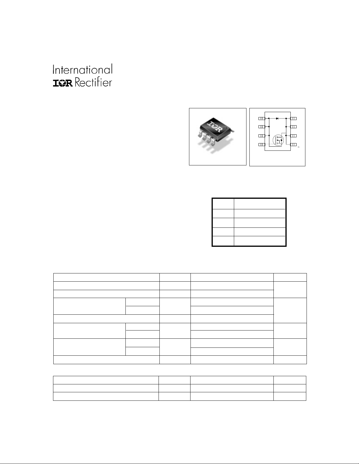
FETKY™ MOSFET / SCHOTTKY DIODE
• Co-Pack N-channel HEXFET
and Schottky Diode
• Ideal for Synchronous Rectifiers in DC-DC
Converters Up to 5A Output
• Low Conduction Losses
• Low Switching Losses
Power MOSFET
A/S
A/S
A/S
1
2
3
4
G
8
K/D
7
K/D
6
K/D
5
K/D
• Low Vf Schottky Rectifier
Description
SO-8
Top View
The FETKY™ family of Co-Pa ck HEXFETMOSFETs and
Schottky diodes offers the designer an innovative, board
space saving solution for switching regulator and power
management applications. HEXFET power MOSFETs
utilize advanced processing techniques to achieve
DEVICE CHARACTERISTICSU
extremely low on-resistance per silicon area. Combining
this technology with International Rectifier’s low forward
drop Schottky rectifiers results in an extremely efficient
device suitable for use in a wide variety of portable
electronics applications.
The SO-8 has been modified through a customized
leadframe for enhanced thermal characteristics. The SO-
IRF7807VD1
R
(on)
DS
Q
G
Q
sw
Q
oss
17mΩ
9.5nC
3.4nC
12nC
8 package is designed for v apor phase, infrared or w a ve
soldering techniques.
Absolute Maximum Ratings
Parameter Symbol Max. Units
Drain-Source Voltage V
Gate-Source Voltage V
Continuous Drain or Source 25°CI
Current (V
≥ 4.5V) 70°C6.6A
GS
Pulsed Drain CurrentQ I
Power DissipationS 25°CP
DS
GS
D
DM
D
70°C1.6
30
±20
8.3
66
2.5
V
W
Schottky and Body Diode 25°C IF (AV) 3.5 A
Average ForwardCurrentT 70°C2.2
Junction & Storage Temperature Range T
J, TSTG
–55 to 150 °C
Thermal Resistance
Parameter Max. Units
Maximum Junction-to-AmbientS R
Maximum Junction-to-Lead R
θJA
θJL
50 °C/W
20 °C/W
www.irf.com 1
03/05/01

IRF7807VD1
Electrical Characteristics
Parameter Min Typ Max Units Conditions
Drain-to-Source BV
Breakdown Voltage
Static Drain-Source R
on Resistance
Gate Threshold Voltage V
Drain-Source Leakage I
Current
Current* 2.0 mA V
Gate-Source Leakage I
Current*
DSS
GSS
Total Gate Charge* Q
Pre-Vth Q
Gate-Source Charge VDS = 16V
Post-Vth Q
Gate-Source Charge
Gate to Drain Charge Q
Switch Chg(Q
+ Qgd) Q
gs2
Output Charge* Q
Gate Resistance R
Turn-on Delay Time t
Rise Time t
d (on)
r
Turn-off Delay Time td
Fall Time t
f
30 –– VVGS = 0V, ID = 250µA
DSS
DS
GS(th)
(on)
17 25 mΩ VGS = 4.5V, ID = 7.0AR
1.0 V VDS = VGS,ID = 250µA
20 µA VDS = 24V, VGS = 0
DS
Tj = 100°C
±100 nA VGS = ±20V
G
GS1
GS2
GD
sw
oss
G
9.5 14 VGS=4.5V, ID=7.0A
2.3
1.0 nC
2.4
3.4 5.2
12 16.8 VDS = 16V, VGS = 0
2.0 Ω
6.3 VDD = 16V, ID = 7.0A
1.2 ns VGS = 5V, RG= 2Ω
(off)
11 Resistive Load
2.2
= 24V, VGS = 0,
Schottky Diode & Body Diode Ratings and Characteristics
Parameter Min Typ Max Units Conditions
Diode Forward Voltage V
SD
0.5 V Tj = 25°C, Is = 1.0A, V
0.39 Tj = 125°C, Is = 1.0A, V
GS
GS
=0VR
Reverse Recovery Time trr 51 ns Tj = 25°C, Is = 7.0A, VDS = 16V
Reverse Recovery Charge Qrr 48 nC di/dt = 100A/µs
Forward Turn-On Time t
Notes:
Q Repetitive rating; pulse width limited by max. junction temperature.
R Pulse width ≤ 400 µs; duty cycle ≤ 2%.
S When mounted on 1 inch square copper board
T 50% Duty Cycle, Rectangular
U
Typical values of R
measured at VGS = 5.0V , IF = 7.0A.
* Device are 100% tested to these parameters.
(on) measured at VGS = 4.5V, QG, QSW and Q
DS
Intrinsic turn-on time is negligible (turn-on is dominated by LS+LD)
on
OSS
2 www.irf.com
=0VR

)
Power MOSFET Selection for DC/DC
Converters
Control FET
Special attention has been given to the power losses
in the switching elements of the circuit - Q1 and Q2.
Power losses in the high side switch Q1, also called
the Control FET, are impacted by the R
MOSFET, but these conduction losses are only about
one half of the total losses.
ds(on)
of the
V
GTH
t1
IRF7807VD1
Drain Current
Gate V oltage
t2
t3
4
1
Power losses in the control switch Q1 are given
by;
P
= P
loss
This can be expanded and approximated by;
P
loss
conduction
I
=
()
rms
+I
+Q
()
g
Q
+
This simplified loss equation includes the terms Q
and Q
charge that is included in all MOSFET data sheets.
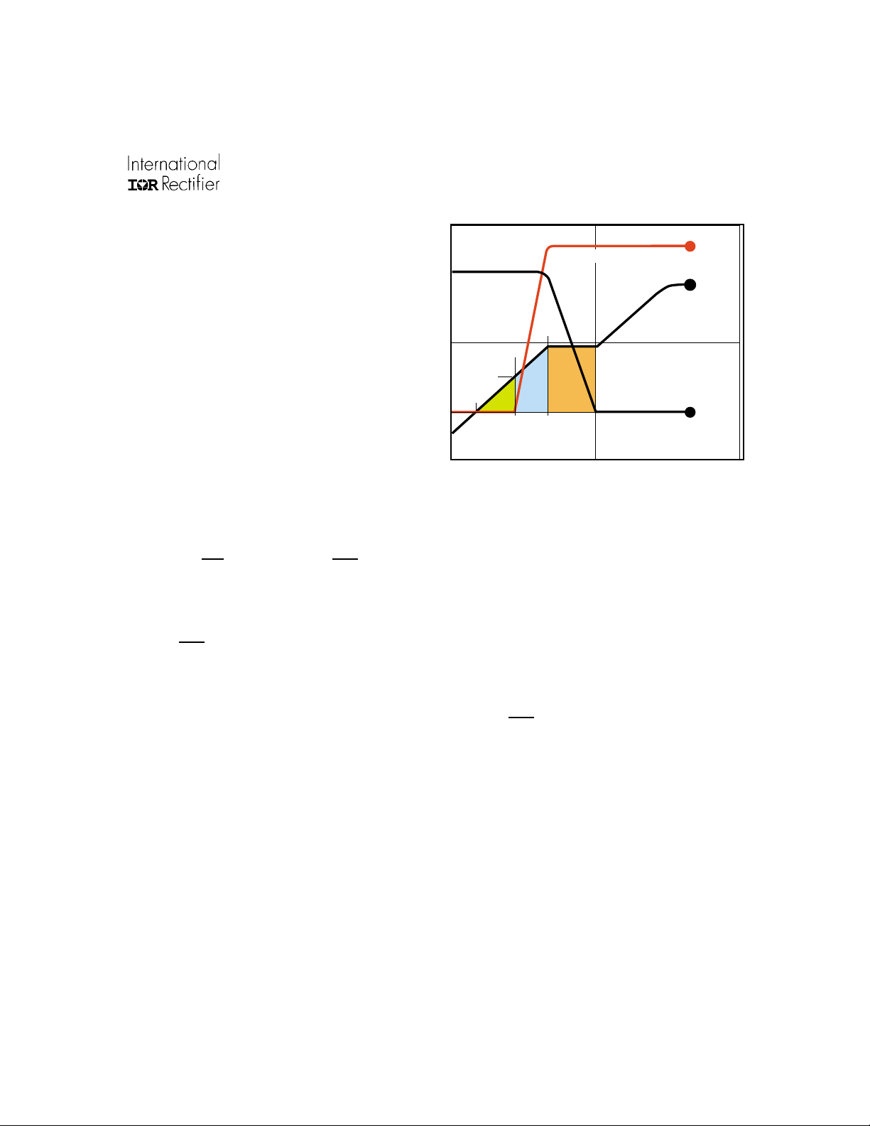
The importance of splitting this gate-source charge
into two sub elements, Q
Fig 1.
the gate driver between the time that the threshold
voltage has been reached (t1) and the time the drain
current rises to I
age begins to change. Minimizing Q
tor in reducing switching losses in Q1.
put capacitance of the MOSFET during every switching cycle. Figure 2 shows how Q
parallel combination of the voltage dependant (nonlinear) capacitance’s Cds and Cdg when multiplied by
the power supply input buss voltage.
which are new to P ower MOSFET data sheets.
oss
Q
is a sub element of traditional gate-source
gs2
Q
indicates the charge that must be supplied by
gs2
Q
is the charge that must be supplied to the out-
oss
+ P
2
R
×
ds(on)
Q
gd
×
×
oss
2
V
×
in
i
g
V
f
×
g
V
×
×
in
(t2) at which time the drain volt-
dmax
switching
f
×
f
and Q
gs1
+ P
+I×
+ P
drive
gs2
oss
output
Q
gs2
×
i
g
, can be seen from
is a critical fac-
gs2
is formed by the
V
f
×
in
gs2
t0
2
*
P
+
output
f
+
(
Drain V oltage
Q
V
×
rr
×
in
GS1QGS2QGD
Q
Figure 1: Typical MOSFET switching waveform
Synchronous FET
The power loss equation for Q2 is approximated
by;
P
P
+Q
*dissipated primarily in Q1.
P
=
loss
conduction
2
I
=
loss
rms
()
()
g
Q
oss
+
2
P
+
drive
R
×
ds(on)
V
×
f
×
g
V
×
×
in
f
www.irf.com 3
 Loading...