

International Rectifier IRF7807D2 Datasheet
PD- 93762
IRF7807D2
FETKY™ MOSFET / SCHOTTKY DIODE
• Co-Pack N-channel HEXFET
and Schottky Diode
• Ideal for Synchronous Rectifiers in DC-DC
Converters up to 5A Output
• Low Conduction Losses
• Low Switching Losses
• Low Vf Schottky Rectifier
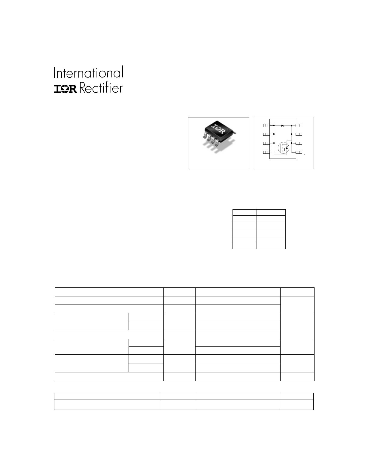
Power MOSFET
SO-8
A/S
A/S
A/S
G
1
2
3
4
Top View
Description
™
The FETKY
family of Co-Pack HEXFET MOSFETs
and Schottky diodes offers the designer an innovative,
board space saving solution for switching regulator and
power management applications. HEXFET power
MOSFETs utilize advanced processing techniques to
achieve extremely low on-resistance per silicon area.
Combining this technology with International Rectifier’s
low forward drop Schottky rectifiers results in an e xtremely
efficient device suitable for use in a wide variety of
portable electronics applications.
Device Features (Max Values)
IRF7807D2
V
DS
30V
RDS(on) 25mΩ
Q
g
Q
SW
Q
oss
14nC
5.2nC
21.6nC
The SO-8 has been modified through a customized
leadframe for enhanced thermal characteristics. The SO8 package is designed for vapor phase, infrared or wave
soldering techniques.
Absolute Maximum Ratings
Parameter Symbol Max. Units
Drain-Source Voltage V
Gate-Source Voltage V
Continuous Drain or Source 25°C I
DS
GS
D
30
±12
8.3
Current (VGS ≥ 4.5V) 70°C 6.6 A
Pulsed Drain Current I
Power Dissipation 25°C P
DM
D
66
2.5
70°C 1.6
Schottky and Body Diode 25°C I
(AV) 3.7 A
F
Average ForwardCurrent 70°C 2.3
Junction & Storage Temperature Range TJ, T
STG
–55 to 150 °C
8
K/D
7
K/D
6
K/D
5
K/D
V
W
Thermal Resistance
Parameter Max. Units
Maximum Junction-to-Ambient R
θJA
50 °C/W
www.irf.com 1
11/8/99
IRF7807D2
Electrical Characteristics
Parameter Min Typ Max Units Conditions
Drain-to-Source V
(BR)DSS
Breakdown Voltage*
Static Drain-Source RDS(on) 17 25 mΩ VGS = 4.5V, ID = 7A
on Resistance*
Gate Threshold Voltage* V
Drain-Source Leakage I
(th) 1.0 V VDS = VGS,ID = 250µA
GS
DSS
Current* 7.2 mA VDS = 24V, VGS = 0V,
30 V VGS = 0V, ID = 250µA
90 µAVDS = 24V, VGS = 0V
Tj = 125°C
Gate-Source Leakage I
GSS
+/- 100 nA VGS = +/-12V
Current*
Total Gate Charge Q
gsync
Synch FET* V
Total Gate Charge Q
gcont
Control FET* V
Pre-Vth Q
gs1
10.5 14 VDS<100mV,
= 5V, ID = 7A
GS
12 17 VDS= 16V,
= 5V, ID = 7A
GS
2.1 VDS = 16V, ID = 7A
Gate-Source Charge
Post-Vth Q
gs2
0.76 nC
Gate-Source Charge
Gate to Drain Charge Q
Switch Charge* Q
(Q
+ Qgd)
gs2
Output Charge* Q
Gate Resistance R
gd
SW
oss
g
2.9
3.66 5.2
17.6 21.6 VDS = 16V, VGS = 0
1.2 Ω
Schottky Diode & Body Diode Ratings and Characteristics
Parameter Min Typ Max Units Conditions
Diode Forward Voltage V
SD
0.54 V Tj = 25°C, Is = 3A, V
0.43 Tj = 125°C, Is = 3A, V
GS
GS
=0V
=0V
Reverse Recovery Time trr 36 ns Tj = 25°C, Is = 7.0A, VDS = 16V
Reverse Recovery Charge Qrr 41 nC di/dt = 100A/µs
Forward Turn-On Time t
Intrinsic turn-on time is negligible (turn-on is dominated by LS+LD)
on
Repetitiv e rating; pulse width limited b y max. junction temperature.
Pulse width ≤ 300 µs; duty cycle ≤ 2%.
When mounted on 1 inch square copper board, t < 10 sec.
50% Duty Cycle , Rectangular
* Devices are 100% tested to these parameters.
2 www.irf.com

IRF7807D2
100
VGS
TOP 4.5V
3.5V
3.0V
BOTTOM 2.5V
10
, Drain-to-Source Current (A)
D
I
380µs PULSE WIDTH
Tj = 25°C
1
0.1 1 10
VDS, Drain-to-Source Voltage (V)
Fig 1. Typical Output Characteristics
70
VGS
TOP 4.5V
60
3.5V
3.0V
2.5V
50
2.0V
BOTTOM 0.0V
40
2.5V
100
VGS
TOP 4.5V
3.5V
3.0V
BOTTOM 2.5V
10
, Drain-to-Source Current (A)
D
I
380µs PULSE WIDTH
1
0.1 1 10
Tj = 150°C
VDS, Drain-to-Source Voltage (V)
Fig 2. Typical Output Characteristics
70
VGS
TOP 4.5V
60
3.5V
3.0V
2.5V
50
2.0V
BOTTOM 0.0V
40
2.5V
30
20
, Source-to-Drain Current (A)
S
I
10
380µs PULSE WIDTH
0.0 V
Tj = 25°C
0
0 0.2 0.4 0.6 0.8 1
VSD, Source-to-Drain Voltage (V)
Fig 3. Typical Reverse Output Characteristics
30
20
, Source-to-Drain Current (A)
S
I
10
O.OV
380µS PULSE WIDTH
Tj = 150°C
0
0 0.2 0.4 0.6 0.8 1
VSD, Source-to-Drain Voltage (V)
Fig 4. Typical Reverse Output Characteristics
www.irf.com 3
 Loading...