International Rectifier IRF7807D1 Datasheet

PD- 93761
IRF7807D1
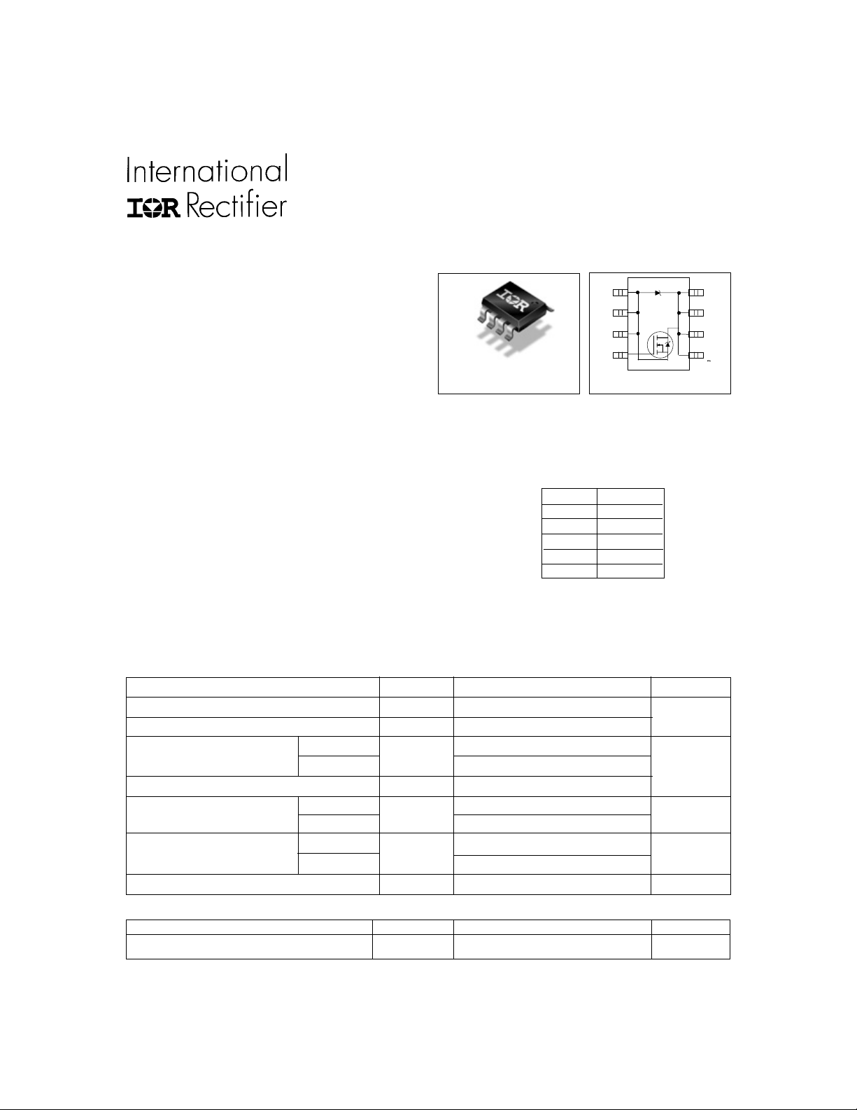
FETKY™ MOSFET / SCHOTTKY DIODE
• Co-Pack N-channel HEXFET
and Schottky Diode
• Ideal for Synchronous Rectifiers in DC-DC
Converters Up to 5A Output
• Low Conduction Losses
• Low Switching Losses
• Low Vf Schottky Rectifier
Power MOSFET
SO-8
A/S
A/S
A/S
G
1
2
3
4
Top View
8
K/D
7
K/D
6
K/D
5
K/D
Description
™
The FETKY
family of Co-Pa ck HEXFETMOSFETs and
Schottky diodes offers the designer an innovativ e , board
space saving solution for switching regulator and power
management applications. HEXFET power MOSFETs
utilize advanced processing techniques to achieve
extremely low on-resistance per silicon area. Combining
this technology with International Rectifier’s low forward
drop Schottky rectifiers results in an extremely efficient
device suitable for use in a wide variety of portable
electronics applications.
Device Features (Max Values)
IRF7807D1
V
DS
R
DS(on)
Q
g
Q
sw
Q
oss
30V
25mΩ
14nC
5.2nC
18.4nC
The SO-8 has been modified through a customized
leadframe for enhanced thermal characteristics. The SO8 package is designed for vapor phase, infrared or wav e
soldering techniques.
Absolute Maximum Ratings
Parameter Symbol Max. Units
Drain-Source Voltage V
Gate-Source Voltage V
Continuous Drain or Source 25°C I
Current (V
≥ 4.5V) 70°C 6.6 A
GS
Pulsed Drain Current I
Power Dissipation 25°C P
DS
GS
D
DM
D
30
±12
8.3
66
2.5
V
W
70°C 1.6
Schottky and Body Diode 25°C I
(AV) 3.5 A
F
Average ForwardCurrent 70°C 2.2
Junction & Storage Temperature Range T
J, TSTG
–55 to 150 °C
Thermal Resistance
Parameter Max. Units
Maximum Junction-to-Ambient R
θJA
50 °C/W
www.irf.com 1
11/8/99

IRF7807D1
Electrical Characteristics
Parameter Min Typ Max Units Conditions
Drain-to-Source V
(BR)DSS
Breakdown Voltage*
Static Drain-Source RDS(on) 17 25 mΩ VGS = 4.5V, ID = 7A
on Resistance*
Gate Threshold V oltage* V
Drain-Source Leakage I
(th) 1.0 V VDS = VGS,ID = 250µA
GS
DSS
Current* 7.2 mA VDS = 24V, VGS = 0V,
30 V VGS = 0V, ID = 250µA
90 µAVDS = 24V, VGS = 0V
Tj = 125°C
Gate-Source Leakage I
GSS
+/- 100 nA VGS = +/-12V
Current*
Total Gate Charge Q
gsync
Synch FET* V
Total Gate Charge Q
gcont
Control FET* V
Pre-Vth Q
gs1
10.5 14 VDS<100mV,
= 5V, ID = 7A
GS
12 17 VDS= 16V,
= 5V, ID = 7A
GS
2.1 VDS = 16V, ID = 7A
Gate-Source Charge
Post-Vth Q
gs2
0.76 nC
Gate-Source Charge
Gate to Drain Charge Q
Switch Charge* Q
(Q
+ Qgd)
gs2
Output Charge* Q
Gate Resistance R
gd
SW
oss
g
2.9
3.66 5.2
15.3 18.4 VDS = 16V, VGS = 0
1.2 Ω
Schottky Diode & Body Diode Ratings and Characteristics
Parameter Min Typ Max Units Conditions
Diode Forward Voltage V
SD
0.5 V Tj = 25°C, Is = 1A, V
0.39 Tj = 125°C, Is = 1A, V
GS
GS
=0V
=0V
Reverse Recovery Time trr 51 ns Tj = 25°C, Is = 7.0A, VDS = 16V
Reverse Recovery Charge Qrr 48 nC di/dt = 100A/µs
Forward Turn-On Time t
Intrinsic turn-on time is negligible (turn-on is dominated by LS+LD)
on
Repetitive rating; pulse width limited by max. junction temperature .
Pulse width ≤ 300 µs; duty cycle ≤ 2%.
When mounted on 1 inch square copper board, t < 10 sec.
50% Duty Cycle, Rectangular
* Devices are 100% tested to these parameters.
2 www.irf.com

IRF7807D1
100
VGS
TOP 4.5V
3.5V
3.0V
BOTTOM 2.5V
10
, Drain-to-Source Current ( A )
D
I
380µs PULSE WIDTH
Tj = 25°C
1
0.1 1 10
VDS, Drain-to-Source Voltage (V)
60
VGS
TOP 4.5V
3.5V
50
3.0V
2.5V
2.0V
BOTTOM 0.0V
40
30
20
, Source-to-Drain Current (A)
S
10
I
380µs PULSE WIDTH
Tj = 25°C
0
0 0.2 0.4 0.6 0.8 1
VSD, Source-to-Drain Voltage (V)
2.5V
0.0V
100
VGS
TOP 4.5V
3.5V
3.0V
BOTTOM 2.5V
10
, Drain-to-Source Current (A)
D
I
380µs PULSE WIDTH
Tj = 150°C
1
0.1 1 10
VDS, Drain-to-Source Voltage (V)
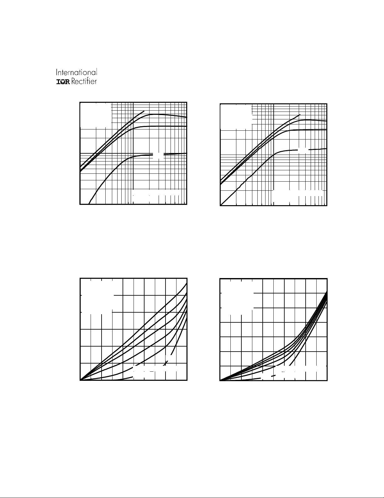
Fig 2. Typical Output CharacteristicsFig 1. Typical Output Characteristics
70
VGS
TOP 4.5V
60
3.5V
3.0V
2.5V
2.0V
50
BOTTOM 0.0V
40
30
20
, Source-to-Drain Current (A)
S
I
10
0
0 0.2 0.4 0.6 0.8 1
VSD, Source-to-Drain Voltage (V)
380µS PULSE WIDTH
Tj = 150°C
0.0V
2.5V
Fig 3. Typical Reverse Output Characteristics
Fig 4. Typical Reverse Output Characteristics
www.irf.com 3
 Loading...