

International Rectifier IRF7752 Datasheet
l Ultra Low On-Resistance
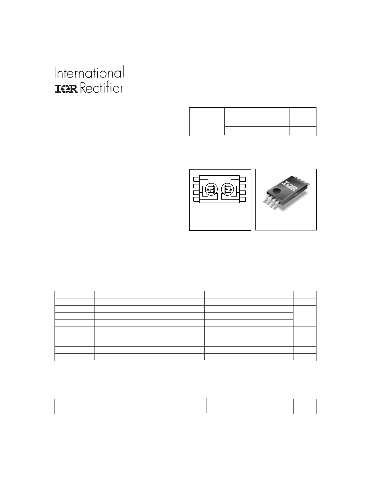
l Dual N-Channel MOSFET
l Very Small SOIC Package
l Low Profile (< 1.1mm)
l Available in Tape & Reel
Description
HEXFET® power MOSFETs from International Rectifier
utilize advanced processing techniques to achieve extremely low on-resistance per silicon area. This benefit,
combined with the ruggedized device design , that International Rectifier is well known for,
with an extremely efficient and reliable device for use
in battery and load management.
The TSSOP-8 package, has 45% less footprint area of the
standard SO-8. This makes the TSSOP-8 an ideal device
for applications where printed circuit board space is at a
premium.
The low profile (<1.1mm) of the TSSOP-8 will allow it to fit
easily into extremely thin application environments such
as portable electronics and PCMCIA cards.
provides thedesigner
PD -94030A
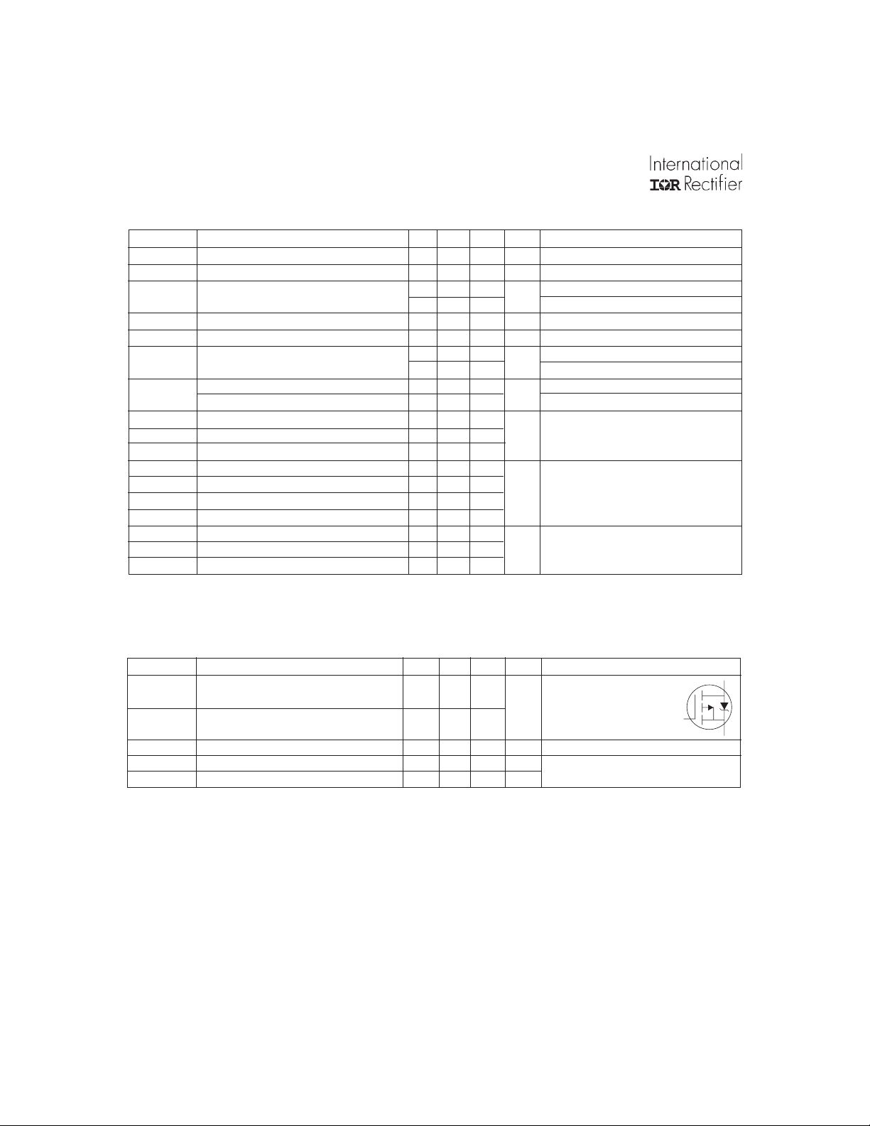
IRF7752
HEXFET® Power MOSFET
V
DSS
30V 0.030@VGS = 10V 4.6A
1
2
3
4
1 = D1
2 = S1
3 = S1
4 = G1
R
max I
DS(on)
0.036@VGS = 4.5V 3.9A
8
7
6
5
8 = D2
7 = S2
6 = S2
5 = G2
TSSOP-8
D
Absolute Maximum Ratings
Parameter Max. Units
V
DS
ID @ TC = 25°C Continuous Drain Current, VGS @ 10V ±4.6
ID @ TC = 70°C Continuous Drain Current, VGS @ 10V ±3.7 A
I
DM
PD @TA = 25°C Power Dissipation 1.0
PD @TA = 70°C Power Dissipation 0.64
V
GS
T
J, TSTG
Drain- Source Voltage 30 V
Pulsed Drain Current ±37
W
Linear Derating Factor 8.0 mW/°C
Gate-to-Source Voltage ± 12 V
Junction and Storage Temperature Range -55 to + 150 °C
Thermal Resistance
Parameter Max. Units
R
θJA
Maximum Junction-to-Ambient 125 °C/W
www.irf.com 1
3/25/01
IRF7752
Electrical Characteristics @ TJ = 25°C (unless otherwise specified)
Parameter Min. Typ. Max. Units Conditions
V
(BR)DSS
∆V
(BR)DSS
R
DS(on)
V
GS(th)
g
fs
I
DSS
I
GSS
Q
g
Q
gs
Q
gd
t
d(on)
t
r
t
d(off)
t
f
C
iss
C
oss
C
rss
Drain-to-Source Breakdown Voltage 30 ––– ––– V VGS = 0V, ID = -250µA
/∆T
Breakdown Voltage Temp. Coefficient ––– 0.030 ––– V/°C Reference to 25°C, ID = 1mA
J
Static Drain-to-Source On-Resistance
––– ––– 0.030 VGS = 10V, ID = 4.6A
––– ––– 0.036 VGS = 4.5V, ID = 3.9A
Ω
Gate Threshold Voltage 0.60 ––– 2.0 V VDS = VGS, ID = 250µA
Forward Transconductance 12 ––– ––– S VDS = 10V, ID = 4.6A
Drain-to-Source Leakage Current
Gate-to-Source Forward Leakage ––– ––– -200 VGS = -12V
Gate-to-Source Reverse Leakage ––– ––– 200 VGS = 12V
––– ––– 20 VDS = 24V, VGS = 0V
––– ––– 100 VDS = 24V, VGS = 0V, TJ = 125°C
µA
nA
Total Gate Charge – – – 9 .0 ––– ID = 4.6A
Gate-to-Source Charge ––– 2.5 ––– nC VDS = 24V
Gate-to-Drain ("Miller") Charge ––– 2.6 ––– VGS = 4.5V
Turn-On Delay Time ––– 7. 2 ––– VDD = 15V
Rise Time ––– 9.1 ––– ID = 1.0A
Turn-Off Delay Time ––– 25 ––– RG = 6.0Ω
ns
Fall Time ––– 11 ––– VGS = 10V
Input Capacitance ––– 861 ––– VGS = 0V
Output Capacitance ––– 210 ––– pF VDS = 25V
Reverse Transfer Capacitance ––– 25 ––– ƒ = 1.0MHz
Source-Drain Ratings and Characteristics
Parameter Min. Typ. Max. Units Conditions
I
S
I
SM
V
SD
t
rr
Q
rr
Continuous Source Current MOSFET symbol
(Body Diode) showing the
Pulsed Source Current integral reverse
(Body Diode) p-n junction diode.
––– –––
––– ––– 37
0.91
A
G
Diode Forward Voltage ––– ––– 1.3 V TJ = 25°C, IS = 0.91A, VGS = 0V
Reverse Recovery Time ––– 25 ––– ns TJ = 25°C, IF = 0.91A
Reverse RecoveryCharge ––– 23 ––– nC di/dt = 100A/µs
Notes:
Repetitive rating; pulse width limited by
When mounted on 1 inch square copper board, t<10 sec
max. junction temperature.
Pulse width ≤ 300µs; duty cycle ≤ 2%.
2 www.irf.com
D
S
IRF7752
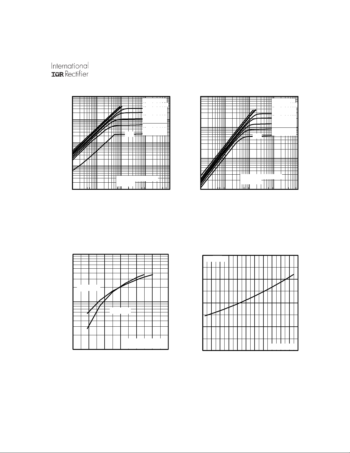
100
10
2.3V
1
0.1
, Drain-to-Source Current (A)
D
I
20µs PULSE WIDTH
Tj = 25°C
0.01
0.01 0.1 1 10 100
VDS, Drain-to-Source Voltage (V)
Fig 1. Typical Output Characteristics
100
VGS
TOP 10.0V
5.0V
4.5V
3.3V
3.0V
2.7V
2.5V
BOTTOM 2.3V
100
10
2.3V
1
, Drain-to-Source Current (A)
D
I
20µs PULSE WIDTH
Tj = 150°C
0.1
0.01 0.1 1 10 100
VDS, Drain-to-Source Voltage (V)
Fig 2. Typical Output Characteristics
2.0
4.6A
I =
D
VGS
TOP 10.0V
5.0V
4.5V
3.3V
3.0V
2.7V
2.5V
BOTTOM 2.3V
1.5
°
T = 150 C
J
10
°
T = 25 C
J
D
I , Drain-to-Source Current (A)
V = 15V
DS
1
2.0 2.3 2.7 3.0 3.3 3.7 4.0
V , Gate-to-Source Voltage (V)
GS
20µs PULSE WIDTH
Fig 3. Typical Transfer Characteristics
1.0
(Normalized)
0.5
DS(on)
R , Drain-to-Source On Resistance
0.0
-60 -40 -20 0 20 40 60 80 100 120 140 160
T , Junction Temperature( C)
J
Fig 4. Normalized On-Resistance
V =
GS
°
10V
Vs. Temperature
www.irf.com 3
 Loading...