

International Rectifier IRF7530 Datasheet
● Trench Technology
● Ultra Low On-Resistance
● Dual N-Channel MOSFET
● Very Small SOIC Package
● Low Profile (<1.1mm)
● Available in Tape & Reel
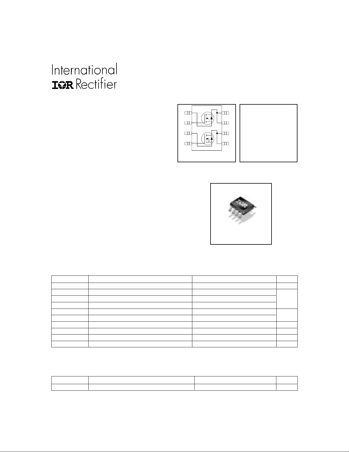
S1
G1
S2
G2
PD-93760B
IRF7530
HEXFET® Power MOSFET
1
2
3
4
8
D1
V
7
D1
6
D2
5
D2
R
DS(on)
= 20V
DSS
= 0.030Ω
Description
Top View
New trench HEXFET power MOSFETs from International
Rectifier utilize advanced processing techniques to achieve
extremely low on-resistance per silicon area. This benefit,
combined with the ruggedized device design that HEXFET
Power MOSFETs are well known for, provides the designer
with an extremely efficient and reliable device for use in a wide
variety of applications.
The new Micro8 package has half the footprint area of the
standard SO-8. This makes the Micro8 an ideal device for
applications where printed circuit board space is at a premium.
The low profile (<1.1mm) of the Micro8 will allow it to fit easily
Micro8
into extremely thin application environments such as portable
electronics and PCMCIA cards.
Absolute Maximum Ratings
Parameter Max. Units
V
DS
ID @ TA = 25°C Continuous Drain Current, VGS @ 4.5V 5.4
ID @ TA= 70°C Continuous Drain Current, VGS @ 4.5V 4.3 A
I
DM
PD @TA = 25°C Power Dissipation 1.3
PD @TA = 70°C Power Dissipation 0.80
E
AS
V
GS
T
J, TSTG
Drain- Source Voltage 20 V
Pulsed Drain Current Q 40
Linear Derating Factor 10 mW/°C
Single Pulse Avalanche EnergyT 33 mJ
Gate-to-Source Voltage ± 12 V
Junction and Storage Temperature Range -55 to + 150 °C
W
Thermal Resistance
Parameter Max. Units
R
θJA
Maximum Junction-to-AmbientS 100 °C/W
www.irf.com 1
02/16/01
IRF7530
Electrical Characteristics @ TJ = 25°C (unless otherwise specified)
Parameter Min. Typ. Max. Units Conditions
V
(BR)DSS
∆V
(BR)DSS
R
DS(on)
V
GS(th)
g
fs
I
DSS
I
GSS
Q
g
Q
gs
Q
gd
t
d(on)
t
r
t
d(off)
t
f
C
iss
C
oss
C
rss
Drain-to-Source Breakdown Voltage 20 ––– ––– VVGS = 0V, ID = 250uA
/∆T
Breakdown Voltage Temp. Coefficient ––– 0.01 ––– V/°C Reference to 25°C, ID = 1mA
J
Static Drain-to-Source On-Resistance
––– ––– 0.030 V
––– ––– 0.045 VGS = 2.5V, ID = 4.6A R
Ω
= 4.5V, ID = 5.4A R
GS
Gate Threshold Voltage 0.60 ––– 1.2 V VDS = VGS, ID = 250µA
Forward Transconductance 13 ––– ––– SVDS = 10V, ID = 5.4A
Drain-to-Source Leakage Current
Gate-to-Source Forward Leakage ––– ––– 100 V
Gate-to-Source Reverse Leakage ––– ––– -100 VGS = -12V
––– ––– 1.0 VDS = 16V, VGS = 0V
––– ––– 25 VDS = 16V, VGS = 0V, TJ = 70°C
µA
nA
GS
= 12V
Total Gate Charge ––– 18 26 ID = 5.4A
Gate-to-Source Charge ––– 3.4 5.1 nC VDS = 16V
Gate-to-Drain ("Miller") Charge ––– 3.4 5.1 VGS = 4.5V R
Turn-On Delay Time ––– 8.5 ––– VDD = 10V
Rise Time ––– 11 ––– ID = 1.0A
Turn-Off Delay Time ––– 36 ––– RG = 6.0Ω
ns
Fall Time ––– 16 ––– RD = 10Ω R
Input Capacitance ––– 1310 ––– VGS = 0V
Output Capacitance ––– 180 ––– pF VDS = 15V
Reverse Transfer Capacitance ––– 150 ––– ƒ = 1.0MHz
Source-Drain Ratings and Characteristics
Parameter Min. Typ. Max. Units Conditions
I
S
I
SM
V
SD
t
rr
Q
rr
Continuous Source Current MOSFET symbol
(Body Diode) showing the
Pulsed Source Current integral reverse
(Body Diode) Q p-n junction diode.
––– –––
1.3
––– ––– 40
A
G
Diode Forward Voltage ––– ––– 1.2 V TJ = 25°C, IS = 1.3A, VGS = 0V R
Reverse Recovery Time ––– 19 29 ns TJ = 25°C, IF = 1.3A
Reverse RecoveryCharge ––– 13 20 nC di/dt = 100A/µs R
Notes:
Q Repetitive rating; pulse width limited by
S When mounted on 1 inch square copper board, t<10 sec
max. junction temperature.
R Pulse width ≤ 400µs; duty cycle ≤ 2%.
T Starting T
RG = 25Ω, I
= 25°C, L = 2.6mH
J
= 5.0A. (See Figure 10)
AS
2 www.irf.com
D
S
IRF7530
100
D
I , Drain-to-Source Current (A)
10
0.1 1 10 100
100
VGS
TOP
7.00V
5.00V
4.50V
3.50V
3.00V
2.70V
2.50V
BOTTOM
2.25V
2.25V
20µs PULSE WIDTH
T = 25 C
J
V , Drain-to-Source Voltage (V)
DS
°
100
D
I , Drain-to-Source Current (A)
10
0.1 1 10 100
VGS
TOP
7.00V
5.00V
4.50V
3.50V
3.00V
2.70V
2.50V
BOTTOM
2.25V
2.25V
20µs PULSE WIDTH
V , Drain-to-Source Voltage (V)
DS
°
T = 150 C
J
Fig 2. Typical Output CharacteristicsFig 1. Typical Output Characteristics
2.0
5.0A
I =
D
°
T = 25 C
J
°
T = 150 C
J
D
I , Drain-to-Source Current (A)
V = 15V
DS
10
2.0 2.5 3.0 3.5 4.0 4.5
V , Gate-to-Source Voltage (V)
GS
20µs PULSE WIDTH
Fig 3. Typical Transfer Characteristics
1.5
1.0
(Normalized)
0.5
DS(on)
R , Drain-to-Source On Resistance
0.0
-60 -40 -20 0 20 40 60 80 100 120 140 160
T , Junction Temperature ( C)
J
Fig 4. Normalized On-Resistance
V =
4.5V
GS
°
Vs. Temperature
www.irf.com 3
 Loading...