SMPS MOSFET
Applications
l High Frequency DC-DC Isolated
Converters with Synchronous Rectification
for Telecom and Industrial use
l High Frequency Buck Converters for
Computer Processor Power
Benefits
l Ultra-Low Gate Impedance
PD - 93937B
IRF3707
IRF3707S
IRF3707L
HEXFET® Power MOSFET
V
DSS
30V 12.5mΩ 62A
R
DS(on)
max I
D
l Very Low R
l Fully Characterized Avalanche Voltage
and Current
DS(on)
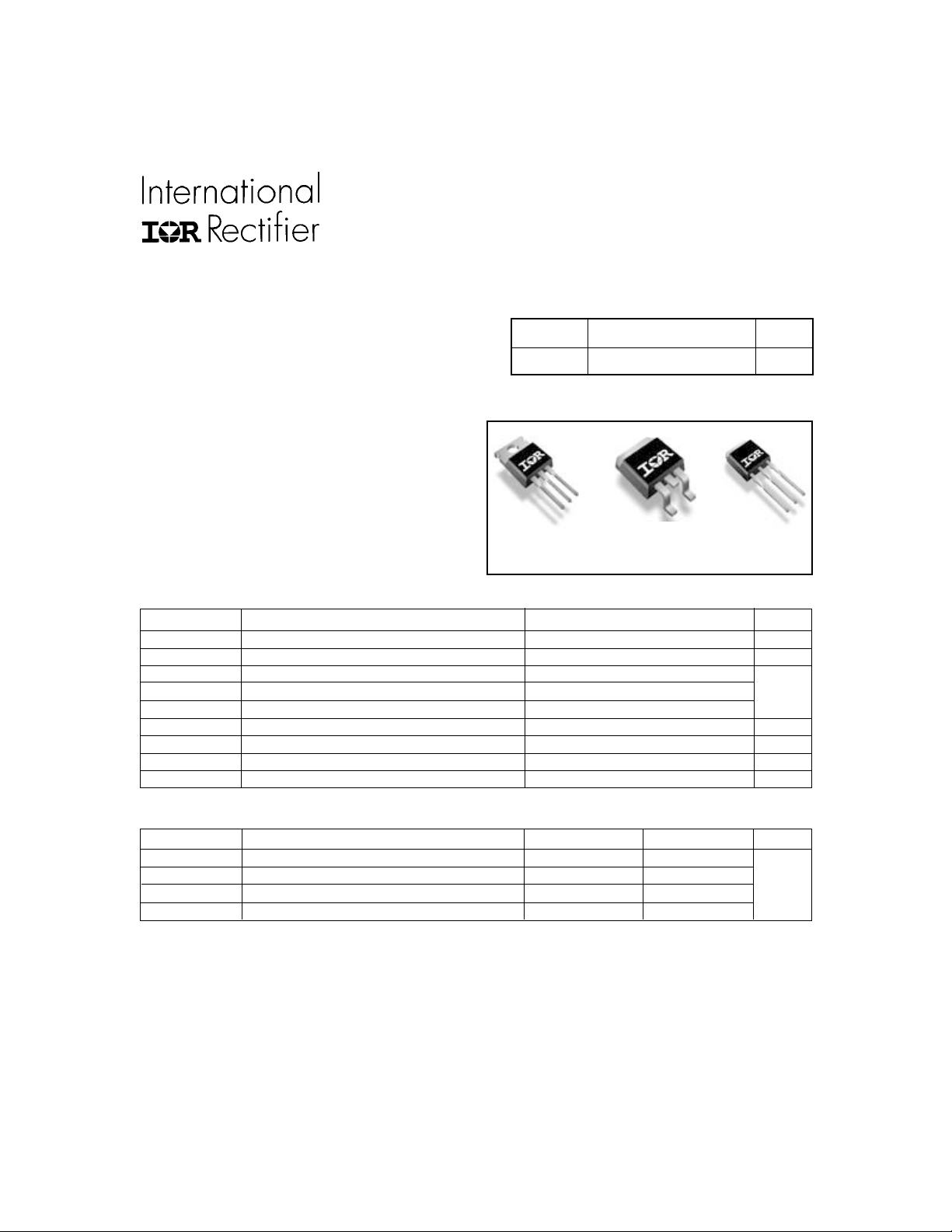
TO-220AB
IRF3707
D2Pak
IRF3707S
TO-262
IRF3707L
Absolute Maximum Ratings
Symbol Parameter Max. Units
V
DS
V
GS
ID @ TC = 25°C Continuous Drain Current, VGS @ 10V 62
ID @ TC = 70°C Continuous Drain Current, VGS @ 10V 52 A
I
DM
PD @TC = 25°C Maximum Power Dissipation 87 W
PD @TC = 70°C Maximum Power Dissipation 61 W
Linear Derating Factor 0.59 mW/°C
TJ , T
STG
Drain-Source Voltage 30 V
Gate-to-Source Voltage ± 20 V
Pulsed Drain Current 248
Junction and Storage Temperature Range -55 to + 175 °C
Thermal Resistance
Parameter Typ. Max. Units
R
θJC
R
θCS
R
θJA
R
θJA
* When mounted on 1" square PCB (FR-4 or G-10 Material) .
For recommended footprint and soldering techniques refer to application note #AN-994
Junction-to-Case ––– 1.73
Case-to-Sink, Flat, Greased Surface 0.50 ––– °C/W
Junction-to-Ambient ––– 62
Junction-to-Ambient (PCB mount)* ––– 40
Notes through are on page 10
www.irf.com 1
8/22/00

IRF3707/3707S/3707L
Static @ TJ = 25°C (unless otherwise specified)
Parameter Min. Typ. Max. Units Conditions
V
(BR)DSS
∆V
(BR)DSS
R
DS(on)
V
GS(th)
I
DSS
I
GSS
Dynamic @ TJ = 25°C (unless otherwise specified)
Symbol Parameter Min. Typ. Max. Units Conditions
g
fs
Q
g
Q
gs
Q
gd
Q
oss
t
d(on)
t
r
t
d(off)
t
f
C
iss
C
oss
C
rss
Drain-to-Source Breakdown Voltage 30 ––– ––– VVGS = 0V, ID = 250µA
/∆T
Breakdown Voltage Temp. Coefficient
J
Static Drain-to-Source On-Resistance
––– 0.027 ––– V/°C Reference to 25°C, ID = 1mA
––– 9.0 12.5 V
––– 12.6 17 VGS = 4.5V, ID = 12A
mΩ
= 10V, ID = 15A
GS
Gate Threshold Voltage 1 .0 ––– 3.0 V VDS = VGS, ID = 250µA
Drain-to-Source Leakage Current
––– ––– 20
––– ––– 100 VDS = 24V, VGS = 0V, TJ = 125°C
Gate-to-Source Forward Leakage ––– ––– 200 V
Gate-to-Source Reverse Leakage ––– ––– -200
VDS = 24V, VGS = 0V
µA
= 16V
GS
nA
V
= -16V
GS
Forward Transconductance 37 ––– ––– SVDS = 15V, ID = 49.6A
Total Gate Charge ––– 19 ––– ID = 24.8A
Gate-to-Source Charge ––– 8.2 ––– nC VDS = 15V
Gate-to-Drain ("Miller") Charge ––– 6.3 ––– VGS = 4.5V
Output Gate Charge ––– 18 27 VGS = 0V, VDS = 15V
Turn-On Delay Time ––– 8.5 ––– VDD = 15V
Rise Time ––– 78 ––– ID = 24.8A
Turn-Off Delay Time ––– 11.8 ––– RG = 1.8Ω
ns
Fall Time ––– 3.3 ––– VGS = 4.5V
Input Capacitance ––– 1990 ––– VGS = 0V
Output Capacitance ––– 707 ––– VDS = 15V
Reverse Transfer Capacitance ––– 50 ––– pF ƒ = 1.0MHz
Avalanche Characteristics
Symbol Parameter Typ. Max. Units
E
AS
I
AR
Single Pulse Avalanche Energy ––– 213 mJ
Avalanche Current ––– 62 A
Diode Characteristics
Symbol Parameter Min. Typ. Max. Units Conditions
I
S
I
SM
V
SD
t
rr
Q
rr
t
rr
Q
rr
Continuous Source Current MOSFET symbol
(Body Diode)
Pulsed Source Current integral reverse
(Body Diode)
Diode Forward Voltage
––– –––
––– –––
62
248
showing the
A
p-n junction diode.
G
––– 0.88 1.3 V TJ = 25°C, IS = 31A, VGS = 0V
––– 0.8 ––– TJ = 125°C, IS = 31A, VGS = 0V
Reverse Recovery Time ––– 39 59 ns TJ = 25°C, IF = 31A, VR=20V
Reverse Recovery Charge ––– 49 74 nC di/dt = 100A/µs
Reverse Recovery Time ––– 42 63 ns TJ = 125°C, IF = 31A, VR=20V
Reverse Recovery Charge ––– 62 93 nC di/dt = 100A/µs
2 www.irf.com
D
S

IRF3707/3707S/3707L
1000
100
3.5V
10
, Drain-to-Source Current (A)
D
I
20µs PULSE WIDTH
Tj = 25°C
1
0.1 1 10 100
VDS, Drain-to-Source Voltage (V)
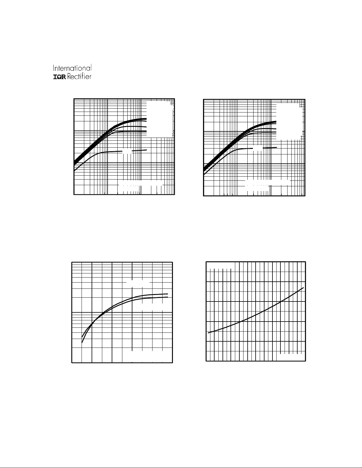
Fig 1. Typical Output Characteristics
1000
VGS
TOP 10.0V
9.0V
8.0V
7.0V
6.0V
5.0V
4.5V
BOTTOM 3.5V
1000
100
3.5V
10
, Drain-to-Source Current (A)
D
I
20µs PULSE WIDTH
Tj = 175°C
1
0.1 1 10 100
VDS, Drain-to-Source Voltage (V)
Fig 2. Typical Output Characteristics
2.5
62A
I =
D
VGS
TOP 10.0V
9.0V
8.0V
7.0V
6.0V
5.0V
4.5V
BOTTOM 3.5V
°
T = 25 C
J
T = 175 C
100
D
I , Drain-to-Source Current (A)
10
3.0 4.0 5.0 6.0 7.0 8.0
V , Gate-to-Source Voltage (V)
GS
J
V = 15V
DS
20µs PULSE WIDTH
Fig 3. Typical Transfer Characteristics
°
2.0
1.5
1.0
(Normalized)
0.5
DS(on)
R , Drain-to-Source On Resistance
0.0
-60 -40 -20 0 20 40 60 80 100 120 140 160 180
T , Junction Temperature( C)
J
Fig 4. Normalized On-Resistance
V =
10V
GS
°
Vs. Temperature
www.irf.com 3
 Loading...