International Rectifier IRF1405S, IRF1405L Datasheet

AUTOMOTIVE MOSFET
PD -93992
IRF1405S
IRF1405L
Typical Applications
● Electric Power Steering (EPS)
● Anti-lock Braking System (ABS)
● Wiper Control
● Climate Control
● Power Door
Benefits
● Advanced Process Technology
● Ultra Low On-Resistance
● Dynamic dv/dt Rating
● 175°C Operating Temperature
● Fast Switching
● Repetitive Avalanche Allowed up to Tjmax
G
HEXFET® Power MOSFET
D
V
= 55V
DSS
R
DS(on)
= 5.3mΩ
ID = 131A
S
Description
Stripe Planar design of HEXFET® Power MOSFETs
utilizes the lastest processing techniques to achieve
extremely low on-resistance per silicon area. Additional
features of this HEXFET power MOSFET are a 175°C
junction operating temperature, fast switching speed
and improved repetitive avalanche rating. These
D2Pak
IRF1405S
TO-262
IRF1405L
benefits combine to make this design an extremely
efficient and reliable device for use in Automotive
applications and a wide variety of other applications.
Absolute Maximum Ratings
Parameter Max. Units
ID @ TC = 25°C Continuous Drain Current, VGS @ 10V 131
ID @ TC = 100°C Continuous Drain Current, VGS @ 10V 93 A
I
DM
PD @TC = 25°C Power Dissipation 200 W
V
GS
E
AS
I
AR
E
AR
dv/dt Peak Diode Recovery dv/dt 5.0 V/ns
T
J
T
STG
Pulsed Drain Current 680
Linear Derating Factor 1.3 W/°C
Gate-to-Source Voltage ± 20 V
Single Pulse Avalanche Energy 590 mJ
Avalanche Current See Fig.12a, 12b, 15, 16 A
Repetitive Avalanche Energy mJ
Operating Junction and -55 to + 175
Storage Temperature Range
Soldering Temperature, for 10 seconds 300 (1.6mm from case )
Mounting Torque, 6-32 or M3 screw 10 lbf•in (1.1N•m)
°C
Thermal Resistance
Parameter Typ. Max. Units
R
θJC
R
θJA
Junction-to-Case ––– 0.75 °C/W
Junction-to-Ambient (PCB mount) ––– 40
www.irf.com 1
1/11/01

IRF1405S/L
Electrical Characteristics @ TJ = 25°C (unless otherwise specified)
Parameter Min. Typ. Max. Units Conditions
V
(BR)DSS
∆V
(BR)DSS
R
DS(on)
V
GS(th)
g
fs
I
DSS
I
GSS
Q
g
Q
gs
Q
gd
t
d(on)
t
r
t
d(off)
t
f
L
D
L
S
C
iss
C
oss
C
rss
C
oss
C
oss
C
eff. Effective Output Capacitance ––– 1500 ––– VGS = 0V, VDS = 0V to 44V
oss
Drain-to-Source Breakdown Voltage 55 –– – –– – V VGS = 0V, ID = 250µA
/∆T
Breakdown Voltage Temp. Coefficient ––– 0.057 ––– V/°C Reference to 25°C, ID = 1mA
J
Static Drain-to-Source On-Resistance ––– 4.6 5.3 mΩ VGS = 10V, ID = 101A
Gate Threshold Voltage 2.0 ––– 4.0 V VDS = 10V, ID = 250µA
Forward Transconductance 69 ––– ––– S VDS = 25V, ID = 110A
Drain-to-Source Leakage Current
––– ––– 20
––– ––– 250 VDS = 44V, VGS = 0V, TJ = 150°C
Gate-to-Source Forward Leakage ––– ––– 200 VGS = 20V
Gate-to-Source Reverse Leakage ––– ––– -200
VDS = 55V, VGS = 0V
µA
nA
VGS = -20V
Total Gate Charge ––– 170 260 ID = 101A
Gate-to-Source Charge ––– 44 66 nC VDS = 44V
Gate-to-Drain ("Miller") Charge ––– 62 93 VGS = 10V
Turn-On Delay Time ––– 13 ––– VDD = 38V
Rise Time ––– 190 ––– ID = 110A
Turn-Off Delay Time ––– 130 ––– RG = 1.1Ω
ns
Fall Time ––– 110 ––– VGS = 10V
4.5
Internal Drain Inductance
Internal Source Inductance ––– –––
––– –––
7.5
Between lead,
6mm (0.25in.)
nH
from package
and center of die contact
Input Capacitance ––– 5480 ––– VGS = 0V
Output Capacitance ––– 1210 ––– pF VDS = 25V
Reverse Transfer Capacitance ––– 280 ––– ƒ = 1.0MHz, See Fig. 5
Output Capacitance ––– 5210 ––– VGS = 0V, VDS = 1.0V, ƒ = 1.0MHz
Output Capacitance ––– 900 ––– VGS = 0V, VDS = 44V, ƒ = 1.0MHz
D
G
S
Source-Drain Ratings and Characteristics
Parameter Min. Typ. Max. Units Conditions
I
S
I
SM
V
SD
t
rr
Q
rr
t
on
Continuous Source Current MOSFET symbol
(Body Diode)
Pulsed Source Current integral reverse
(Body Diode)
––– –––
––– –––
131
680
showing the
A
p-n junction diode.
G
Diode Forward Voltage ––– ––– 1.3 V TJ = 25°C, IS = 101A, VGS = 0V
Reverse Recovery Time ––– 88 1 30 n s TJ = 25°C, IF = 101A
Reverse RecoveryCharge – –– 250 380 nC di/dt = 100A/µs
Forward Turn-On Time Intrinsic turn-on time is negligible (turn-on is dominated by LS+LD)
2 www.irf.com
D
S

IRF1405S/L
1000
100
10
D
I , Drain-to-Source Current (A)
1
0.1 1 10 100
1000
VGS
TOP
15V
10V
8.0V
7.0V
6.0V
5.5V
5.0V
BOTTOM
4.5V
4.5V
20µs PULSE WIDTH
T = 25 C
J
V , Drain-to-Source Voltage (V)
DS
°
T = 25 C
J
°
T = 175 C
J
1000
100
D
I , Drain-to-Source Current (A)
10
0.1 1 10 100
VGS
TOP
15V
10V
8.0V
7.0V
6.0V
5.5V
5.0V
BOTTOM
4.5V
4.5V
20µs PULSE WIDTH
T = 175 C
V , Drain-to-Source Voltage (V)
DS
°
J
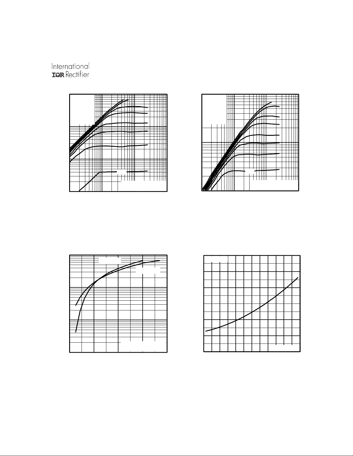
Fig 2. Typical Output CharacteristicsFig 1. Typical Output Characteristics
3.0
°
2.5
169A
I =
D
100
10
D
I , Drain-to-Source Current (A)
V = 25V
DS
1
4 6 8 10 12
V , Gate-to-Source Voltage (V)
GS
20µs PULSE WIDTH
Fig 3. Typical Transfer Characteristics
2.0
1.5
(Normalized)
1.0
0.5
DS(on)
R , Drain-to-Source On Resistance
0.0
-60 -40 -20 0 20 40 60 80 100 120 140 160 180
T , Junction Temperature ( C)
J
Fig 4. Normalized On-Resistance
V =
10V
GS
°
Vs. Temperature
www.irf.com 3

IRF1405S/L
100000
10000
1000
C, Capacitance(pF)
100
1 10 100
V
= 0V, f = 1 MHZ
GS
C
= C
= C
= C
gs
gd
ds
Ciss
Coss
Crss
+ Cgd, C
+ C
gd
iss
C
rss
C
oss
VDS, Drain-to-Source Voltage (V)
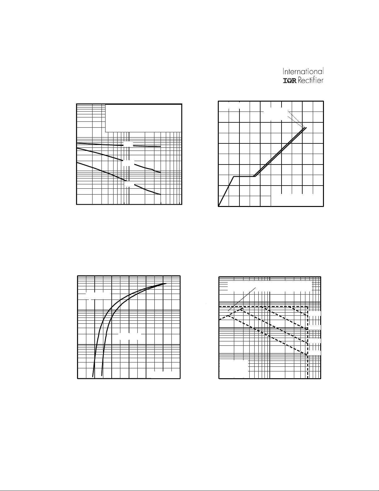
Fig 5. Typical Capacitance Vs.
Drain-to-Source Voltage
1000
°
T = 175 C
J
100
SHORTED
ds
20
I =
101A
D
16
12
8
4
GS
V , Gate-to-Source Voltage (V)
0
0 60 120 180 240 300
Q , Total Gate Charge (nC)
G
V = 44V
DS
V = 27V
DS
FOR TEST CIRCUIT
SEE FIGURE
Fig 6. Typical Gate Charge Vs.
Gate-to-Source Voltage
10000
1000
OPERATION IN THIS AREA LIMITED
BY R
DS(on)
13
10us
100us
1ms
10ms
°
T = 25 C
J
10
SD
I , Reverse Drain Current (A)
V = 0 V
1
0.0 0.5 1.0 1.5 2.0 2.5 3.0
V ,Source-to-Drain Voltage (V)
SD
GS
Fig 7. Typical Source-Drain Diode
100
D
I , Drain Current (A)I , Drain Current (A)
10
°
= 25 C
C
T T= 175 C
Single Pulse
1
1 10 100
°
J
V , Drain-to-Source Voltage (V)
DS
Fig 8. Maximum Safe Operating Area
Forward Voltage
4 www.irf.com
 Loading...