

International Rectifier IRDC3847-P1V2 User Manual

IRDC3847-P1V2
SupIRBuck
TM
USER GUIDE FOR IR3847 EVALUATION BOARD
DESCRIPTION
The IR3847 is a synchronous buck
converter, providing a compact, high
performance and flexible solution in a small
5mmx6mm QFN package.
Key features offered by the IR3847 include
internal Digital Soft Start, precision 0.6V
reference voltage, Power Good, thermal
protection, programmable switching
frequency, Enable input, input under-voltage
lockout for proper start-up, enhanced line/
load regulation with feed forward, external
frequency synchronization with smooth
clocking, internal LDO, true differential
remote sensing and pre-bias start-up.
A thermally compensated output over-current
protection function is implemented by sensing
the voltage developed across the on-resistance
of the synchronous rectifier MOSFET for
optimum cost and performance.
This user guide contains the schematic and bill
of materials for the IR3847 evaluation board.
The guide describes operation and use of the
evaluation board itself. Detailed application
information for IR3847 is available in the
IR3847 data sheet.
BOARD FEATURES
• V
= +12V (+ 13.2V Max), No Vcc required.
in
= +1.2V @ 0- 25A
• V
out
• F
=1000kHz
s
• L= 0. 15uH
• C
= 5x22uF (ceramic 1206) + 1x330uF (electrolytic)
in
• C
=7x22uF (ceramic 0805)
out
2/13/2012
This evaluation board is a preliminary version meant for the engineering evaluation of the IR3847. Based on the results of the
continuing evaluation, this board can evolve and change without notice
Confidential
1
IRDC3847-P1V2
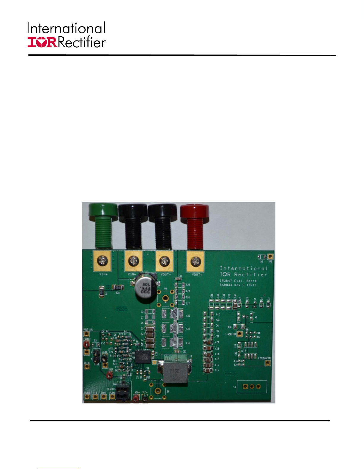
CONNECTIONS and OPERATING INSTRUCTIONS
A well regulated +12V input supply should be connected to VIN+ and VIN-. A maximum of 25A load should
be connected to VOUT+ and VOUT-. The inputs and output connections of the board are listed in Table I.
IR3847 needs only one input supply and internal LDO generates Vcc from Vin. If operation with external Vcc
is required, then R33 should be removed and external Vcc can be applied between Vcc+ and Vcc- pins. Vin
pin and Vcc pins should be shorted together for external Vcc operation by installing R35.
This version of the demoboard was built with a previous revision of the IR3847 for which Vp was pin 14 and
Vref was pin 15. However, in the new revision, these pins have been interchanged in order to allow easier
bypass of the Vref pin. The consequence of this is that the Vp input on the board should be considered Vref
and the Vref input on the board should be considered Vp.
The board is configured for remote sensing. If local sense is desired, R8 should be uninstalled and R16
should be installed instead.
External Enable signal can be applied to the board via exposed Enable pad and R18 should be removed for
this purpose.
Table I. Connections
Connection Signal Name
VIN+ Vin (+12V)
VIN- Ground of Vin
Vout+ Vout(+1.2V)
Vout- Ground for Vout
Vcc+ Vcc Pin
Vcc- Ground for Vcc input
Enable Enable
PGood Power Good Signal
AGnd Analog ground
2/13/2012
This evaluation board is a preliminary version meant for the engineering evaluation of the IR3847. Based on the results of the
continuing evaluation, this board can evolve and change without notice
Confidential
2
IRDC3847-P1V2
CONNECTIONS and OPERATING INSTRUCTIONS
LAYOUT
The PCB is a 6-layer board. All of layers are 2 Oz. copper. The IR3847 and most of the passive
components are mounted on the top side of the board.
Power supply decoupling capacitors and feedback components are located close to IR3847. The
feedback resistors are connected to the output of the remote sense amplifier of the IR3847 and are
located close to the IR3847. To improve efficiency, the circuit board is designed to minimize the l ength
of the on-board power ground current path. Separate power ground and analog ground are used and
may be connected together using a 0 ohm resistor at one of three possible locations. It is preferred to
use one of R43 or R44.
Vin
Gnd
Gnd
Vo
Top View
2/13/2012
This evaluation board is a preliminary version meant for the engineering evaluation of the IR3847. Based on the results of the
continuing evaluation, this board can evolve and change without notice
Confidential
3
IRDC3847-P1V2
Vout+
PVin-
PVin+
1
1
R30
R31
0 ohm
0 ohm
PVin
R18
1
Enable
Vp
25V 330uF
C1
330uF
+
C2
22uF
C3
22uF
C4
22uF
C5
22uF
C6
N/S
Ceramic cap 16V 5X22uF 1206
C7
N/S
C24
0.1uF
C31
N/S
C32
N/S
C56
N/S
C55
N/S
49.9K
R35
N/S
VCC
39.2K
R19
R8
Vp
1
R20
C39
C25
C57
0
R33
1
Vref
0
C11
150pF
Vout
Vo
N/S
N/S
L1
N/S
C38
SWs
1uF
0
R28
0.1uF
0.1uF
26
2
C37
22uF
Boot
PGnd
PVin
1
Vin
Vin
17
Enable
3
Vp
15
U1
FB
RSo
8
7
9
C26
10nF
Vcc+
R1
1K
1
C15
C16
C17
C18
C19
C20
C27
C28
C29
C30
C33
150nH PCDC1008-R15E MO
1
SW
22
SW
SW21SW23SW20SW24SW
Vcc18Comp
R17
1
PGD
VCC
Vout-
1
Vo
Vo
C14
0.1uF
22uF
22uF
22uF
22uF
22uF
22uF
N/S
N/S
N/S
6X22uF/805/6.3V+1X22uF/805/6.3V (transient schematic)
N/S
0.1uF
Vo_R_P
R15
23.2K
Vsns
Vout
R32
23.2K
13
6
32
25
SW
RS+
Vsns
IR3847
Rt/Sync
OCSelect
PGD
4
5
16
PGD
10K
1
PGDPU
OCSelect
2 3
4
JUMPER 2
C51
N/S
+
C34
N/S
+
C36
N/S
+
C35
N/S
+
C22
N/S
C21
N/S
C41
N/S
C40
N/S
C43
N/S
C42
N/S
C44
N/S
C45
N/S
Vo_R_N
R10
0
0
R11
C53
N/S
C50
N/S
RS-
12
PGnd
29
PGnd
10
PGnd
27
LGnd
11
Vref
Vp
14
R9
23.2K
Rt/Sync
N/S
C68
4pin jumper
C66
10uF
1
R16
R6
C8
2200pF
R4
84.5
Fb
N/S
N/S
R3
R29
R14
R34
0
Agnd
Vcc-
Ground and Signal ( “analog” ) Ground
Single point of connection between Power
0
N/S
R43
N/S
20
R2
1
BODE
JUMPER 2
C54
N/S
Vsns
2.67K
N/S
R21
2.61K
Fb
R44
N/S
R27
VPB
N/S
M3
R26
1
Vout_Adj
Vout
D2
1 2
1
Optional "1-bit VID" ci rcuit
N/S
C52
N/S
N/S
Optional Pre-Bias test circuit
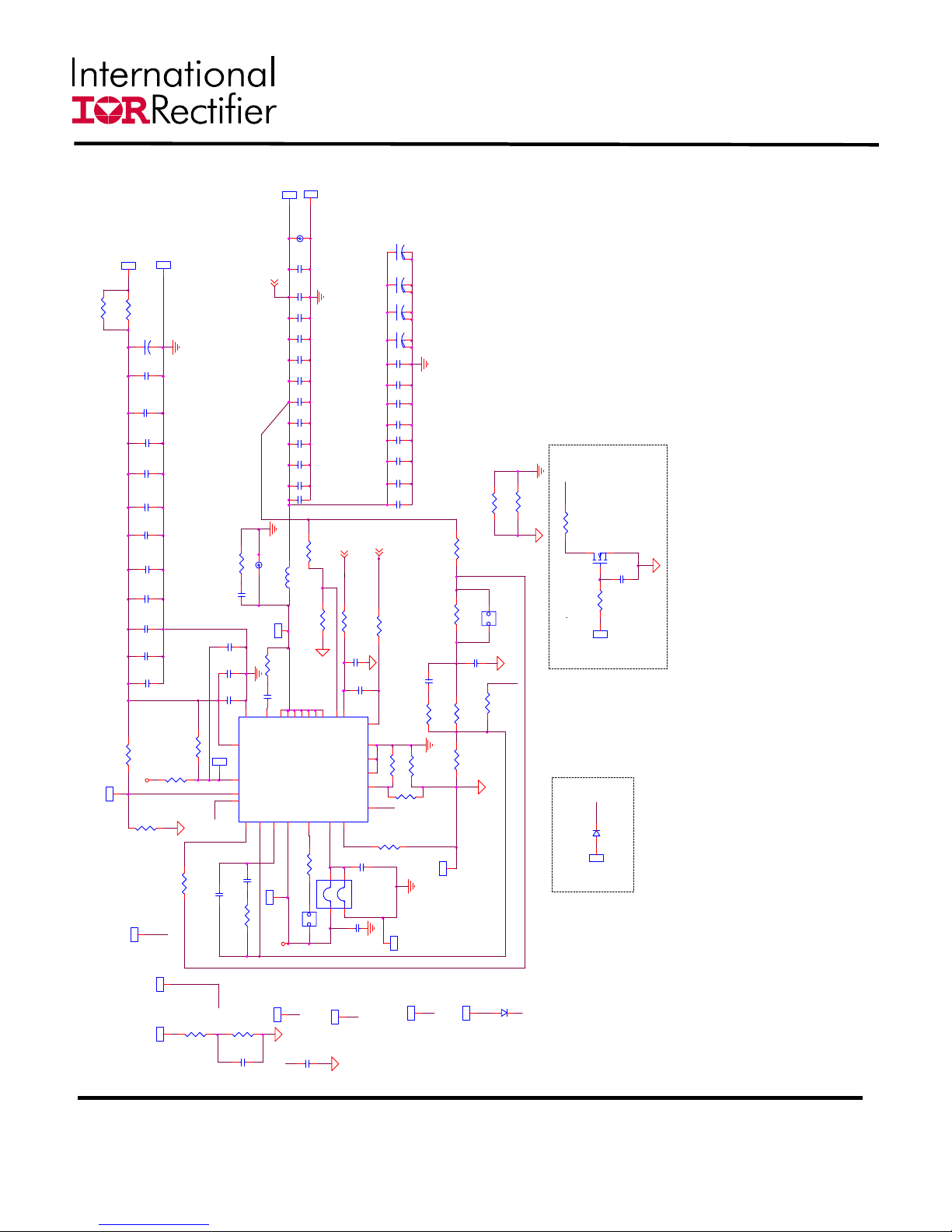
Fig. 1: Schematic of the IR3847 evaluation board
1
Vref
VDDQ
Vref
1
Vp
N/S
R40
N/S
R41
C9
100n
Sctrl
1
Sctrl
Vref
C10
N/S
2/13/2012
This evaluation board is a preliminary version meant for the engineering evaluation of the IR3847. Based on the results of the
continuing evaluation, this board can evolve and change without notice
D3
N/S
Sync
PGD
1
PGood
PGDPU
1
PGDPU
Sync
Rt/Sync
12
1
Confidential
4
 Loading...