

International Rectifier IRDC38063-P1V2 User Manual

IRDC38063-P1V2
SupIRBuck
TM
USER GUIDE FOR IR38063 EVALUATION BOARD
DESCRIPTION
The IR38063 is a synchronous buck
converter with a PMBus interface, providing
a compact, high performance and flexible
solution in a small 5mmx7mm PQFN
package.
Key features offered by the IR38063 include
I2C/PMBus configurability of output voltage,
soft-start, input UVLO, input overvoltage
protection, output overvoltage protection,
output overcurrent protection, Power Good,
thermal protection and switching frequency.
Additionally, the IR38063 also features
enhanced line/ load regulation with feed
forward, external frequency synchronization
with smooth clocking, internal LDO, true
differential remote sensing and pre-bias
start-up.
A temperature and bias compensated output
over-current protection function is implemented
by sensing the voltage developed across the
on-resistance of the synchronous rectifier
MOSFET for optimum cost and performance.
This user guide contains the schematic and bill
of materials for the IR38063 evaluation board.
The guide describes operation and use of the
evaluation board itself. Detailed application
information for IR38063 is available in the
IR38063 data sheet.
BOARD FEATURES
• PVin = +12V (+ 13.2V Max), No Vcc required.
• V
= +1.2V @ 0-25A
out
• F
=600kHz
s
• L= 0.215uH
• Cin= 4x22uF (ceramic 1206) + 1x330uF (electrolytic, optional)
• C
=7x47uF (ceramic 0805)
out
3/21/2017
1
IRDC38063-P1V2
CONNECTIONS and OPERATING INSTRUCTIONS
A well regulated +12V input supply should be connected to PVin+ and PVin-. A maximum of 25A load should
be connected to VOUT+ and VOUT-. The inputs and output connections of the board are listed in Table I.
IR38063 needs only one input supply and internal LDO generates Vcc from PVin. Another internal LDo
generates the 1.8V needed by the internal digital circuits. If operation with external Vcc is required, then R25
should be removed and external Vcc can be applied between Vcc+ and Vcc- pins. Vin pin and Vcc pins
should be shorted together for external Vcc operation by installing R24. For tracking operation R27 should
be populated with a 0 ohm resistor. For normal, non-tracking operation, R27 should not be populated
and a 100 kOhm resistor should be connected from the Track_En pin to P1V8.
The board is configured for remote sensing. If local sense is desired, R8 should be uninstalled and R16
should be installed instead.
I2C/PMBus communication is established through the 4 pin header which allows connection to the
SCL/SDA/SALERT and GND lines from the host/dongle. For proper operation in digital communications
mode, R35 must always be populated.
External Enable signal can be applied to the board via exposed Enable pad and R18 should be removed for
this purpose.
Connection Signal Name
PVin+ PVin (+12V)
Table I. Connections
PVin- Ground of PVin
Vout+ Vout(+1.2V)
Vout- Ground for Vout
Vcc+ Vcc Pin
Vcc- Ground for Vcc input
Enable Enable
PGood Power Good Signal
LAYOUT
The PCB is a 6-layer board. All of layers are 2 Oz. copper. The IR38063 and most of the passive
components are mounted on the top side of the board. Power supply decoupling capacitors and
feedback components are located close to IR38063. The feedback resistors are connected to the
output of the remote sense amplifier of the IR38063 and are located close to the IR38063. To improve
efficiency, the circuit board is designed to minimize the length of the on-board power ground current
path. Separate power ground and analog ground are used and may be connected together using a 0
ohm resistor.
3/21/2017
2
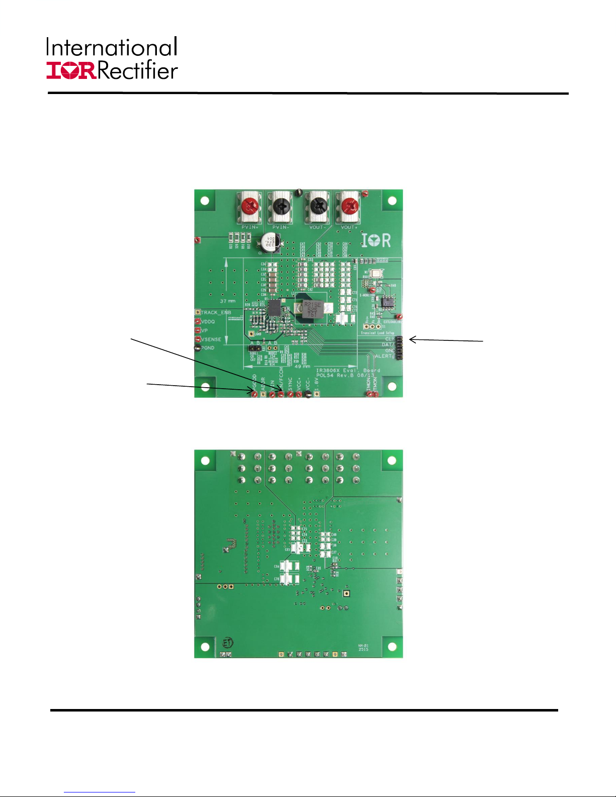
CONNECTION DIAGRAM
IRDC38063-P1V2
Enable
PGood
PVin
Vout
Top View
I2C / PMBus
Communication
3/21/2017
Bottom View
3
IRDC38063-P1V2
R29N/S
U1
IR38063
Vin
21
LGnd
13
Rt/Sy nc
14
Vcc
22
Comp
7
Vsns
5
PGnd
12
SCL/OCSet
19
FB
6
Boot
2
PGood
11
PVin
1
RS-
9
RS+
10
RSo
8
SW
24
3
Track_En
Vp
4
En/FCC M
15
SDA/IMON18SAlert/TMON
17
ADDR
16
P1V8
20
NC1
23
NC2
26
R30 N/S
R25
0
R31
4.99K
En/FCC M
1
R8
20
SDA/IMON
VDDQ
GND
SAlert/TMON
SDA
SDA/IM ON
CLK
DATA
J1
R40
0
R36
50
SCL
VIN
R27
N/S
Vcc
R24 N/S
SCL/OC
C35
1uF
VCC+
1
VCC
VIN
1
Vsns
VIN
Vsense
1
VCC
C80
10uF
BODE2
12
PGood
1
R23 4.99K
R51
0 ohm
R52
0 ohm
Vout_+
1
Vout_-
1
BODE1
12
R39
0
ALERT#
VCC-
1
R18
49.9K
R19
7.5K
C38
N/S
C28
N/S
C40
N/S
C39
N/S
R22
0 ohm
R29 and R30 are unpopulated because our USB/I2C
converter dongle has on-board pullups.
R26
0 ohm
PGND
1
C32
22uF
C29
22uF
C31
22uF
C30
22uF
C37
N/S
C10
0.1uF
+
C1
330uF
PVin-
123456
C36
0.1uF
C34
N/S
C33
N/S
Vout-
123456
PVin+
123456
Vout+
123456
VCC
IMON
1
R33
N/S
TMON
1
SAlert/TM ON
R34
N/S
SCL/OC
PVin
Sync
Rt/Sy nc
Sync
1
R9
3.83K
R28
N/S
Track_Enb
1
C61
N/S
C62
N/S
C53
0.1uF
L1
215 nH PCDC1008-R215EMO
R35
0
C54
N/S
R10
0
Fb
C67
N/S
C59
N/S
C60
N/S
C57
N/S
C58
N/S
R38
N/S
C56
N/S
C55
N/S
SWs
1
SW
R16
N/S
R4
182
R2
5.62K
C52
N/S
Vsns
R6
20
C51
N/S
C50
N/S
R58
N/S
C49
47uF
+
C76
N/S
C48
47uF
1.8V
1
C47
47uF
Vsns
7X47uF/805/6.3V
R15
N/S
+
C77
N/S
+
C65
N/S
R41
0
+
C66
N/S
C46
47uF
C8
2200pF
R14
0
C45
47uF
R11
0
R32
N/S
C44
47uF
C43
47uF
Vo_R_P
R37
0
Vo_R_N
C42
0.1uF
ADDR
Rt/Sy nc
C41
2.2uF
Vp
1
R60
100K
R20
N/S
R21
N/S
R3
N/S
ADDR
ADDR
1
LGnd
1
Vout
C26
22nF
R1
1.21K
C11
390pF
R59
N/S
C27
N/S
1
VDDQ
1
3/21/2017
Single point of connection between Power
Ground and Signal ( “analog” ) Ground
R60 is not present in evaluation boards older than Revision C
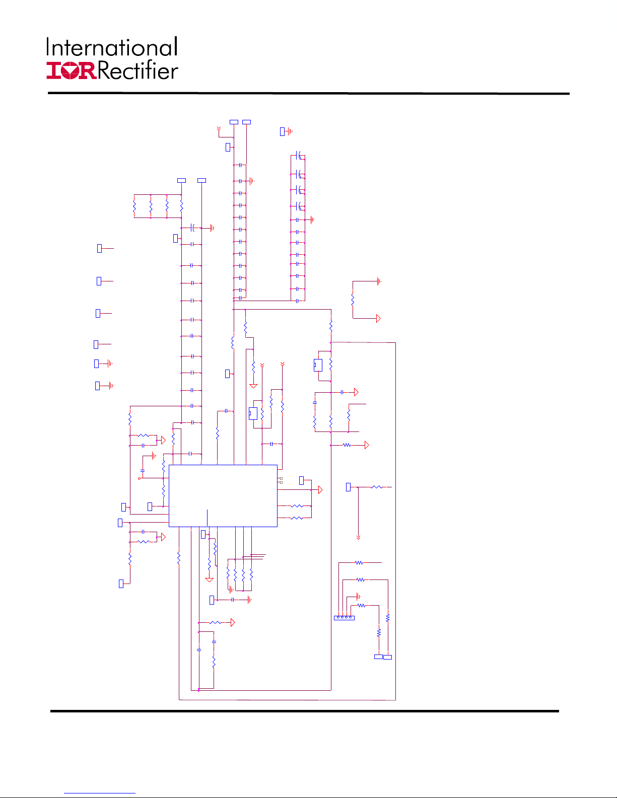
Fig. 1: Schematic of the IR38063 evaluation board
4
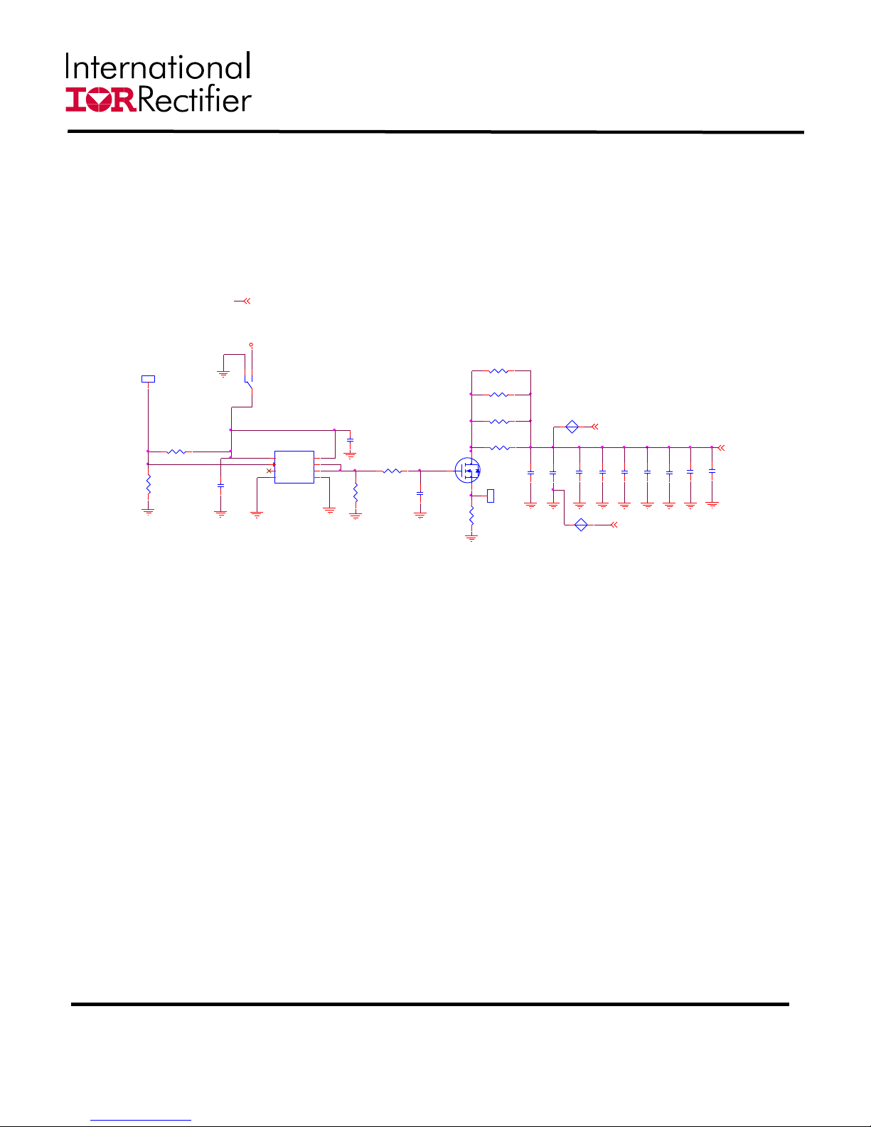
Schematic for Transient Load set up
Vout
S3 should be in position
1-2 to enable transient load
R50
20m
C75
N/S
C71
N/S
C70
N/S
C76
N/S
C68
10u
R42
0.2
R43
0.2
R44
0.2
R46
0.2
R47
1.5K
ExtLoadCt rl
1
M1
IRF6721
U2
MIC4452/SO8
VS
1
IN
2
GND4GND
5
OUT1
6
OUT2
7
VS
8
N/A
3
R45
N/S
R49
10K
S1
SW
2 1
3
C69
0.1uF
C78
0.1uF
R48
10K
Vout
C79
100p
C77
N/S
Vo_R_P
Vo_R_N
VCC
I-Monitor
1
C72
N/S
C73
N/S
C74
N/S
KC10
KC20
Vout
IRDC38063-P1V2
3/21/2017
5
 Loading...