

International Rectifier IRDC3073EVAL User Manual

IRU3073 EVALUATION BOARD USER GUIDE
SPECIFICATION DATAINTRODUCTION
The IRU3073 controller IC is designed to provide a low
cost synchronous Buck regulator for on-board DC to DC
converter for multiple output applications.
The outputs can be programmed as low as 0.8V for low
voltage applications.
Selectable over-current protection is provided by using
external MOSFET's on-resistance for optimum cost and
performance.
This device features a programmable frequency set from
200KHz to 400KHz, under-voltage lockout for all input
supplies, an external programmable soft-start function
as well as output under-voltage detection that latches off
the device when an output short is detected.
Switcher:
VIN = 5V
VOUT1 = 2.5V
IOUT1 = 8A
DVOUT = 50mV
FS = 200KHz
IRDC3073EVAL
Linear
Regulator:
VIN = 2.5V
(from switch)
VOUT2 = 1.6V
IOUT2 = 2A
Supply Voltage:
VCC = VC = 12V
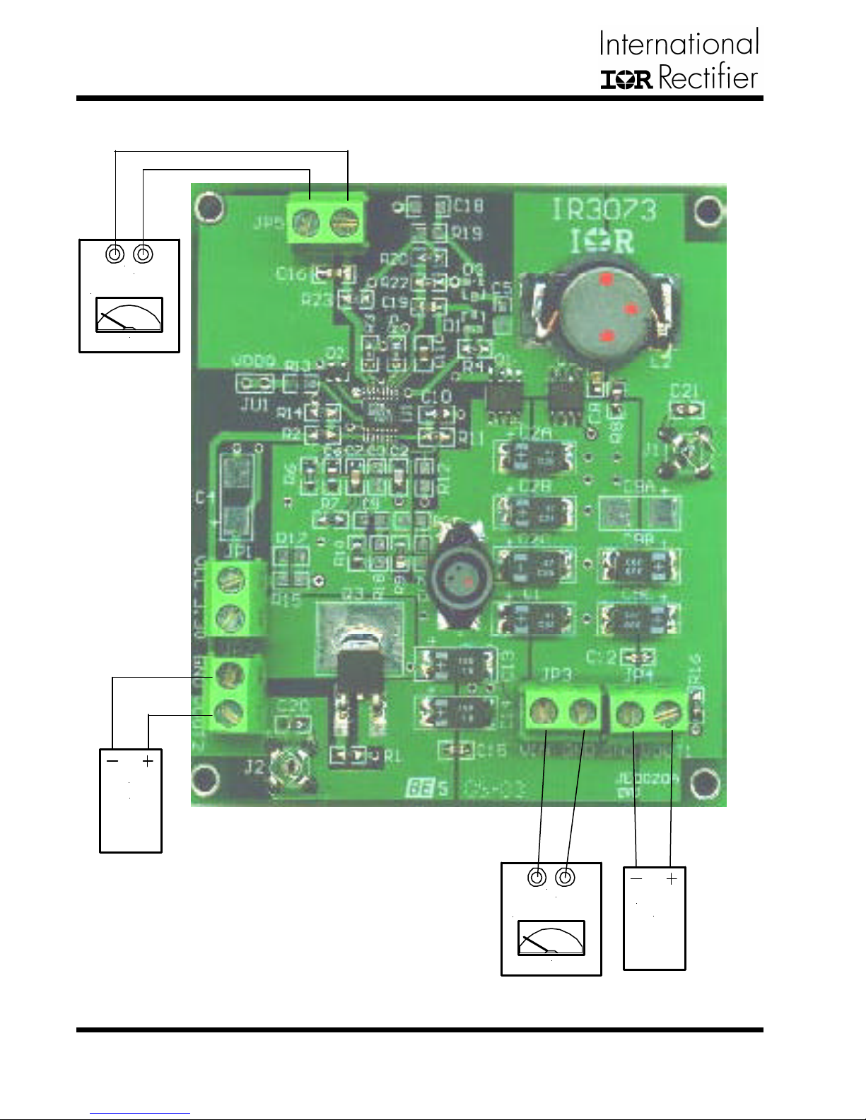
INPUT/OUTPUT CONNECTIONS
The following is the input/output connections:
Inputs:
JP3: Input (+5V), Gnd
JP1: Input (+12V)
Outputs:
JP4: VOUT1 (+2.5V), Gnd
JP2: VOUT2 (+1.6V), Gnd
Note: For proper operation, +5V supply should ramp up first.
The connection points is shown in Figure 1. Connect the
power supply cables according to this figure, minimize
wire lengths to reduce losses in the wire. Test point J1
provides easy connections for the oscilloscope voltage
probe to monitor the output voltage.
Rev. 1.0
06/30/03
www.irf.com
1
IRDC3073EVAL
CONNECTION DIAGRAM
Gnd
+12V
Power Supply
1A Supply
Load2
2A
Figure 1 - Connection diagram of evaluation-board for IRU3073.
2
www.irf.com
Gnd
+5V
Power Supply
10A Supply
Load1
0 - 10A
Rev. 1.0
06/30/03
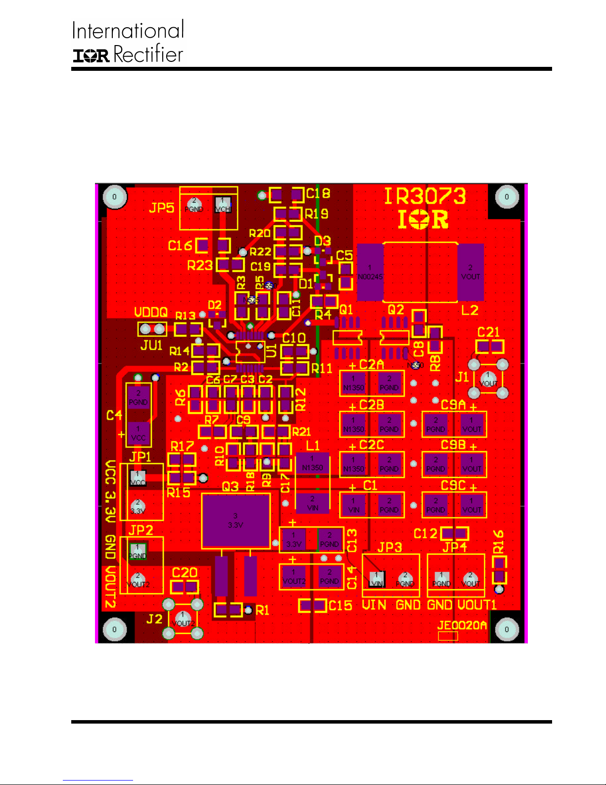
LAYOUT
The four layers for IRU3073 evaluation board are shown
in Figures 2.1-2.4. The layout is designed both for direct
FET package and SOIC package for power MOSFETs.
The input capacitors are all located close to the
MOSFETs. All the decoupling capacitors and feedback
components are located close to IC. The feedback re-
IRDC3073EVAL
sistors are tied to the output voltage at the point of regulation.
The middle layers are dedicated to Power Ground and
Analog Ground. Analog Ground is kept separated from
the Power Ground and it is connected at a single point
as shown in figure 2.3.
Figure 2.1 - Top layer of evaluation-board for IRU3073.
Rev. 1.0
06/30/03
www.irf.com
3
 Loading...