

Page 1

IRDC3821
SupIRBuck
TM
USER GUIDE FOR IR3821 EVALUATION BOARD
DESCRIPTION
The IR3821 is a synchronous buck
converter, providing a compact, high
performance and flexible solution in a small
5mmx6mm Power QFN package.
Key features offered by the IR3821 include
programmable soft-start ramp, precision
0.6V reference voltage, programmable
Power Good
600kHz switching frequency requiring no
external component, input under-voltage
lockout for proper start-up, and pre-bias
start-up.
, thermal protection, fixed
An output over-current protection function is
implemented by sensing the voltage developed
across the on-resistance of the synchronous
rectifier MOSFET for optimum cost and
performance.
This user guide contains the schematic and bill
of materials for the IR3821 evaluation board.
The guide describes operation and use of the
evaluation board itself. Detailed application
information for IR3821 is available in the
IR3821 data sheet.
BOARD FEATURES
Vin= +12V (13.2V Max)
•
• V
= +1.8V @ 0- 7A
out
• L=1.0uH
• C
=3x10uF (ceramic 1206) + 330uF (electrolytic)
in
• C
=6x22uF (ceramic 0805)
out
Rev 0.1
01/07/2008
1
Page 2
IRDC3821
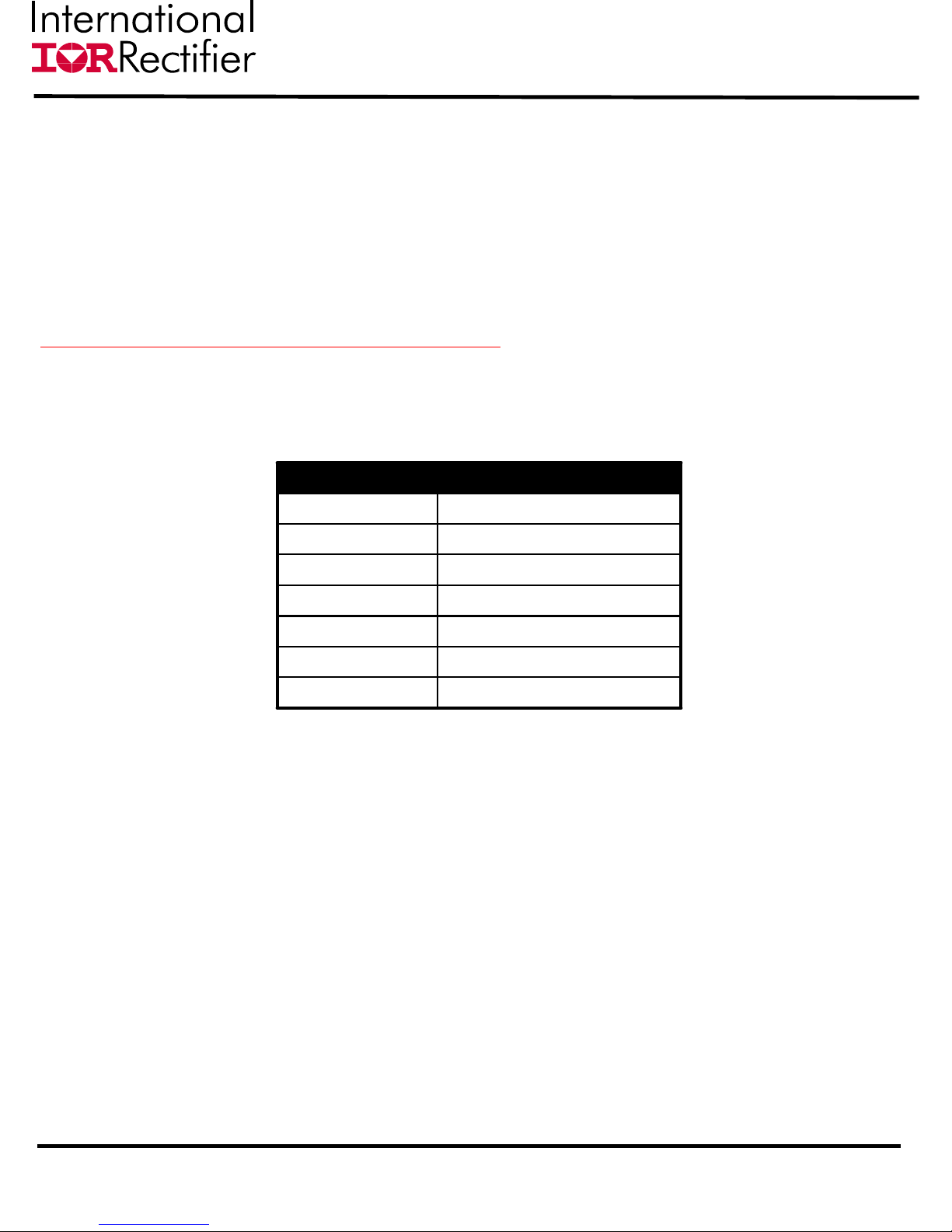
CONNECTIONS and OPERATING INSTRUCTIONS
A well regulated +12V input supply should be connected to VIN+ and VIN-. A maximum 7A load should be
connected to VOUT+ and VOUT-. The connection diagram is shown in Fig. 1 and inputs and outputs of the
board are listed in Table I.
IR3821 has two input supplies, one for biasing (Vcc) and the other as input voltage (Vin). These inputs are
connected on the board with a zero ohm resistor (R15). Separate supplies can be applied to these inputs.
Vcc input cannot be connected unless R15 is removed.
and it would be connected to Vcc+ and Vcc-.
Table I. Connections
Signal NameConnection
Vcc input should be a well regulated 5V-12V supply
(+12V)VIN+
V
in
VIN-
VOUT-
Ground of V
Optional Vcc inputVcc+
Ground for Optional Vcc inputVcc-
Ground of V
V
(+1.8V)VOUT+
out
Power Good SignalP_Good
in
out
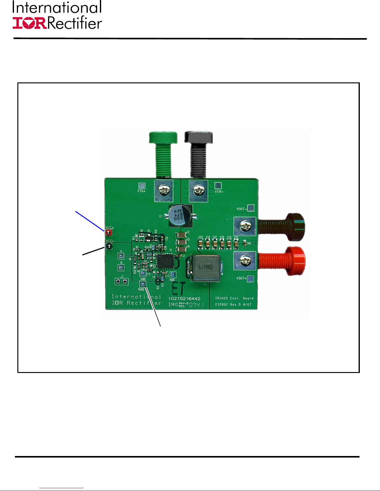
LAYOUT
The PCB is a 4-layer board. All of layers are 2Oz. copper. The IR3821 SupIRBuck and all of the
passive components are mounted on the top side of the board.
Power supply decoupling capacitors, the charge-pump capacitor and feedback components are located
close to IR3821. The feedback resistors are connected to the output voltage at the point of regulation
and are located close to SupIRBuck.
To improve efficiency, the circuit board is designed to minimize the length of the on-board power ground
current path.
Rev 0.1
01/07/2008
2
Page 3
Connection Diagram
IRDC3821
V
CC+
GROUND
Vin= +12v
GROUND
GROUND
Fig. 1: Connection diagram of IR3821 evaluation board
Rev 0.1
01/07/2008
P
Good
V
OUT
= +1.8v
3
Page 4
IRDC3821
Fig. 2: Board layout, top overlay
Fig. 3: Board layout, bottom overlay (rear view)
Rev 0.1
01/07/2008
4
Page 5
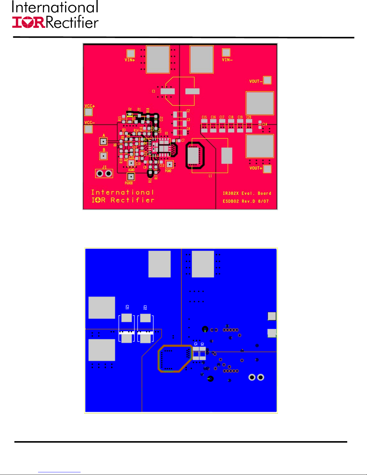
IRDC3821
AGND
Plain
Single point
connection
between AGND
and PGND.
Fig. 4: Board layout, mid-layer I
PGND
Plain
Fig. 5: Board layout, mid-layer II
Rev 0.1
01/07/2008
5
Page 6

IRDC3821
Vin+
Vin+
1
Vin
Vin-
1
1
+
C1
330uF
C7
0.1uF
C2
10uF
C3
10uF
C4
10uF
C5
N/S
C6
N/S
Vin-
1
Vout+
Vout
1
Vout-
Vout+
1
L1
1.0uH
C12
0.1uF
Vout-
1
1
C14
0.1uF
C20
22uF
C19
22uF
C18
22uF
+
C17
22uF
C22
N/S
+
C16
22uF
C21
N/S
C15
22uF
Ground and Signal ( “analog” ) Ground
Single point of connection between Power
B
R15
0
R12
6.98K
VCC
1
PGND
11
Vcc+
Vcc-
12
C24
560pF
13
14
U1
Vsns1FB2AGnd1
C26
1000pF
R1 21k
R9
0
R10
Open
Vin
Hg
Vc
COMP
3
D2
Open
R18
BAT54S
Open
3
C25
0.1uF
R14
10.0k
C11
22pF
R16
3.09k
12
1
1
12
D1
10
SW
PGnd
AGnd3
15
PGood
9
AGnd2
5
1
Vcc
8
C13
VCC
OCset
SS
7
6
C10
0.22uF
J1
SS
IR3821
4
C23
Open
Agnd
C9
Open
C8
180pF
R4
1.96K
1uF
R17
10K
VCC
1
R6 20
A
1
R2
60.4k
R3
30.1K
Fig. 6: Schematic of the IR3821 evaluation board
Rev 0.1
01/07/2008
PGood
1
6
Page 7

IRDC3821
Bill of Materials
Item Quantity Designator Value Description Size Manufacturer Mfr. Part Number
1 1 C1 330uF
2 3 C2 C3 C4 10uF Ceramic, 16V, X7R, 10% 1206 Panasonic ECJ-3YX1C106K
34
4 1 C10 0.22uF Ceramic , 10V, X5R, 10% 0603 Panasonic ECJ-1VB1A224K
5 1 C8 180pF Ceramic, 50V, NPO, 5% 0603 Murata GRM1885C1H181JA01
6 1 C11 22pF Ceramic , 50V, NPO, 5% 0603 Murata GRM1885C1H220JA01
7 1 C13 1uF Ceramic, 16V, X5R, 10% 0603 Panasonic ECJ-1VB1C105K
86
9 1 C24 560pF Ceramic, 50V, NPO, 5% 0603 Murata GRM1885C1H561JA01
10 1 C26 1000pF Ceramic, 50V, NPO, 5% 0603 Murata GRM1885C1H102JA01
11 1 D1 BAT54S Diode Schottky ,40V, 200mA SOT-23 Fairchild BAT54S
12 1 L1 1.0uH
13 1 R1 21.0K Thick film, 1/10W , 1% 0603 Vishey/Dale CRCW060321K0FKEA
14 1 R3 30.1K Thick film, 1/10W , 1% 0603 Vishey/Dale CRCW060330K1FKEA
15 1 R2 60.4K Thick film, 1/10W , 1% 0603 Vishey/Dale CRCW060360K4FKEA
16 1 R4 1.96K Thick film, 1/10W , 1% 0603 Vishey/Dale
17 1 R6 20 Thick film, 1/10W, 1% 0603 Vishey/Dale CRCW060320R0FKEA
18 2 R9 R15 0 Thick film, 1/10W , 1% 0603 Vishey /Dale CRCW06030000Z0EA
19 1 R12 6.98K Thick film, 1/10W , 1% 0603 Vishey/Dale CRCW06036K98FKEA
20 2 R14, R17 10K Thick film, 1/10W, 1% 0603 Vishey/Dale CRCW060310K0FKEA
21 1 R16 3.09K Thick film, 1/10W , 1% 0603 Vishey/Dale
22 1 U1 IR3821
23 2 - -
24 1 - -
25 1 - -
C7 C12 C14
C25
C15 C16 C17
C18 C19 C20
0.1uF Ceramic, 50V, X7R, 10% 0603 Panasonic ECJ-1VB1H104K
22uF Ceramic, 6.3V, X5R, 20% 0805 Panasonic ECJ-2FB0J226M
SMD Electrolytic, 25V, 20%
SMT Inductor, 2.3mOhm,
20%
600kHz, 7A, SupIRBuck
Module
Banana Jac k, Insulated
Solder Terminal, Black
Banana Jac k- Insulated
Solder Terminal, Red
Banana Jac k- Insulated
Solder Terminal, Green
SMD Panasonic
11.5x
10mm
5x6mm
-
-
-
Delta MPL105-1R0
International
Rec tifier
Johnson
Components
Johnson
Components
Johnson
Components
EEV-FK1E331P
CRCW06031K96FKEA
CRCW06033K09FKEA
IR3821
105-0853-001
105-0852-001
105-0854-001
Rev 0.1
01/07/2008
7
Page 8

TYPICAL OPERATING WAVEFORMS
Vin=Vcc=12.0V, Vo=1.8V, Io=0-7A, Room Temperature, No Air Flow
IRDC3821
Vin
Iout
Fig. 7: Start up at 7A Load
Ch
, Ch2:VSS, Ch3:V
1:Vin
Vss
, Ch4:I
out
Vout
out
Vin
Fig. 8: Start up at 7A Load,
Ch
, Ch2:VSS, Ch3:V
1:Vin
PGood
Vout
, Ch4:V
out
Vss
PGood
Fig. 9: Pre-Bias Start up, 0A Load
Ch
, Ch2:VSS, Ch3:V
1:Vin
Fig. 11: Inductor node at 7A load
Ch
:LX, Ch4:I
1
out
Rev 0.1
01/07/2008
out
Fig. 10: Output Voltage Ripple, 7A load
Ch
3
: V
out ,Ch4
: I
out
Fig. 12: Short (Hiccup) Recovery
Ch
2:VSS
, Ch3:V
out
8
Page 9

TYPICAL OPERATING WAVEFORMS
Vin=Vcc=12V, Vo=1.8V, Io=3.5A-7A, Room Temperature, No Air Flow
IRDC3821
Fig. 13: Transient Response, 3.5A to 7A step
Rev 0.1
01/07/2008
Ch
3:Vout
, Ch4:I
out
9
Page 10

TYPICAL OPERATING WAVEFORMS
Vin=Vcc=12V, Vo=1.8V, Io=7A, Room Temperature, No Air Flow
IRDC3821
Fig. 14: Bode Plot at 7A load shows a bandwidth of 62 kHz and phase margin of 51 degrees
Rev 0.1
01/07/2008
10
Page 11

TYPICAL OPERATING WAVEFORMS
Vin=12V, Vo=1.8V, Io=0-7A, Room Temperature, No Air Flow
90
80
70
Efficiency (%)
60
50
0.51.52.53.54.55.56.5
Load Current (A)
IRDC3821
Efficiency VCC=VIN=12V Efficiency VIN=12V@VCC=5V
Fig.15: Efficiency versus load current
2.5
2.0
1.5
1.0
Power Loss (W)
0.5
0.0
0.0 1.0 2.0 3.0 4.0 5.0 6.0 7.0
Load Current (A)
Power Loss VCC=VIN=12V Power Loss VIN = 12V@VCC = 5V
Fig.16: Power loss versus load current
Rev 0.1
01/07/2008
11
Page 12

THERMAL IMAGES
Vin=Vcc=12V, Vo=1.8V, Io=7A, Room Temperature, No Air Flow
IRDC3821
Fig. 17: Thermal Image at 7A load
Test point 1 is the IR3821
Rev 0.1
01/07/2008
12
Page 13

IRDC3821
PCB Metal and Components Placement
The lead lands (the 11 IC pins) width should be equal to the nominal part lead width. The minimum
lead to lead spacing should be ≥ 0.2mm to minimize shorting.
Lead land length should be equal to the maximum part lead length + 0.3 mm outboard extension. The
outboard extension ensures a large and inspectable toe fillet.
The pad lands (the 4 big pads other than the 11 IC pins) length and width should be equal to
maximum part pad length and width. However, the minimum metal to metal spacing should be no less
than 0.17mm for 2 oz. Copper; no less than 0.1mm for 1 oz. Copper and no less than 0.23mm for 3 oz.
Copper.
Rev 0.1
01/07/2008
Page 14

IRDC3821
Solder Resist
It is recommended that the lead lands are Non Solder Mask Defined (NSMD). The solder resist
should be pulled away from the metal lead lands by a minimum of 0.025mm to ensure NSMD
pads.
The land pad should be Solder Mask Defined (SMD), with a minimum overlap of the solder resist
onto the copper of 0.05mm to accommodate solder resist mis-alignment.
Ensure that the solder resist in between the lead lands and the pad land is ≥ 0.15mm due to the
high aspect ratio of the solder resist strip separating the lead lands from the pad land.
Rev 0.1
01/07/2008
Page 15

IRDC3821
Stencil Design
• The Stencil apertures for the lead lands should be approximately 80% of the area of the
lead lads. Reducing the amount of solder deposited will minimize the occurrences of lead
shorts. If too much solder is deposited on the center pad the part will float and the lead
lands will be open.
• The maximum length and width of the land pad stencil aperture should be equal to the
solder resist opening minus an annular 0.2mm pull back to decrease the incidence of
shorting the center land to the lead lands when the part is pushed into the solder paste.
Rev 0.1
01/07/2008
Page 16

IRDC3821
IR WORLD HEADQUARTERS: 233 Kansas St., El Segundo, California 90245, USA Tel: (310) 252-7105
This product has been designed and qualified for the Consumer market.
Rev 0.1
01/07/2008
TAC Fax: (310) 252-7903
Visit us at www.irf.com for sales contact information
Data and specifications subject to change without notice. 11/07
 Loading...