

Page 1

USER GUIDE FOR IR3651 EVALUATION BOARD
DESCRIPTION
IRDC3651
The IR3651 is a high voltage PWM
controller designed for high performance
synchronous Buck DC/DC applications . The
IR3651 drives a pair of external NMOSFETS using a programmable switching
frequency up to 400kHz allows flexibility to
tune the operation of the IC to meet system
level requirements, and synchronization
allows the simplification of system level filter
design. The output voltage can be precise ly
regulated using the internal 1.25V re ference
voltage for low voltage applications.
Protection functions such as under voltage
lockout and hiccup current limit are pro vided
to give required system level security in the
event of fault conditions.
CONNECTIONS
J2: VIN= 48V
This user guide contains the schematic and
bill of materials for the IR3651 evaluation
board. The guide describes operation and use
of the evaluation board itself. Detailed
application information for the IR3651
integrated circuit is available in the IR3651
data sheet.
Evaluation Board Specifications:
VIN= 48V, tolerance 10%
V
= 3.3V at 10A
OUT
FS= 100kHz
Rev 1.1
12/20/2006
OUT
= 3.3V
J3: V
J4, J7: GROUND
J5: Shutdown control input
J6: Sync input
J1: External 12V supply option.
RD-0616
1
Page 2
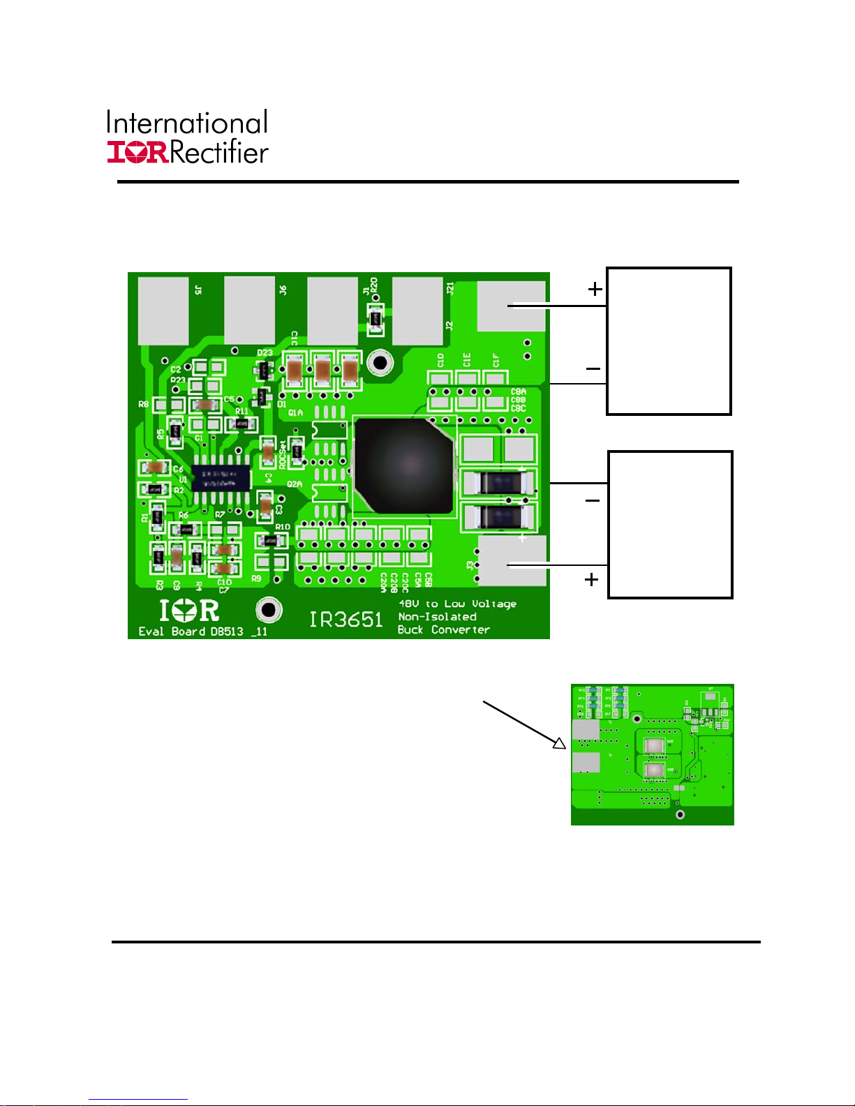
CONNECTION DIAGRAM
IRDC3651
48V
Power
Supply
Load:
3.3V@
0A to 10A
Note: Ground connection pads are located on
the bottom side of the circuit board.
Figure 1 – Connections to IR3651 evaluation board
for default configuration .
Rev 1.1
12/20/2006
RD-0616
2
Page 3
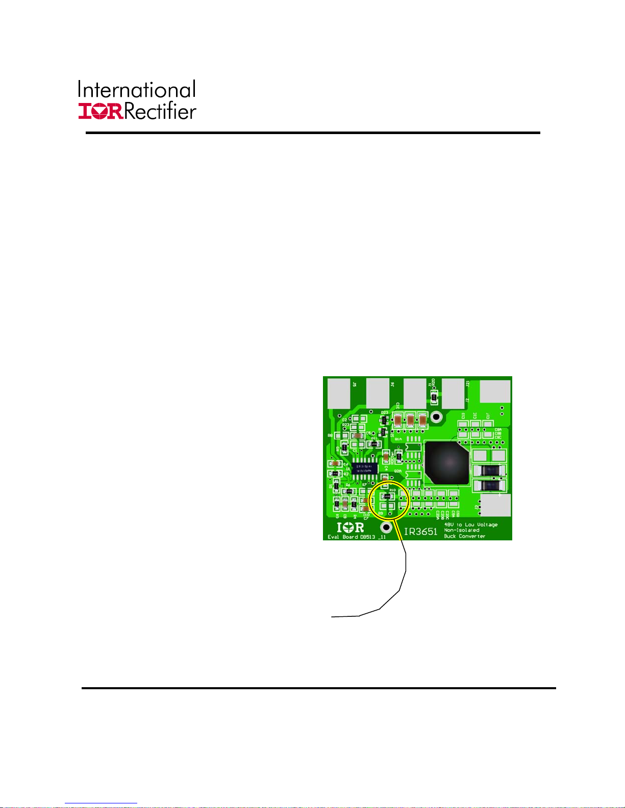
IRDC3651
CIRCUIT LAYOUT - TOP LAYER
The PCB is a 4-layer FR4 board. The IR3651 IC
and the associated passive components are
mounted on the top side of the board.
Solder pads for off-board connections to various
power supply options and control signals are
placed on the top layer.
Off-board connections to ground are available on
the bottom layer.
Power supply decoupling capacitors, the charge
pump capacitor and feedback components are
located close to the IR3651 IC. The feedback
resistors are connected to the output voltage at
the point of regulation and are located close to
the IC.
Two alternatives are provided for implementation
of the required single point of connection
between Signal Ground and Power ground.
Install a zero ohm resistor at location R10 to
implement the shortest available connection
between the grounds. Installation of R10 is the
minimum–noise solution and is the default. If
R10 is removed and R9 is installed, an
approximation of remote voltage sensing is
available. Remote sensing will minimize volt age
error due to ground currents, but may be more
vulnerable to high-frequency noise.
Two different MOSFET configurations can be
used: eight-pin SOIC packages on the top side
of the board or MX-packaged DirectFets on the
bottom side of the board. The bottom–side
location of the DirectFet packages allows
convenient mounting of heat sinking devices
The input and output energy storage
capacitors and the power inductor are placed
close to the MOSFET packages.
To improve efficiency, the circuit board is
designed to minimize the length of the onboard power ground current path.
Either R9 or R10 (default) must be
installed to implement the required single
point of connection between Signal
Ground and Power Ground.
Figure 2 – Top layer of the IR3651 evaluation board.
Rev 1.1
12/20/2006
RD-0616
3
Page 4
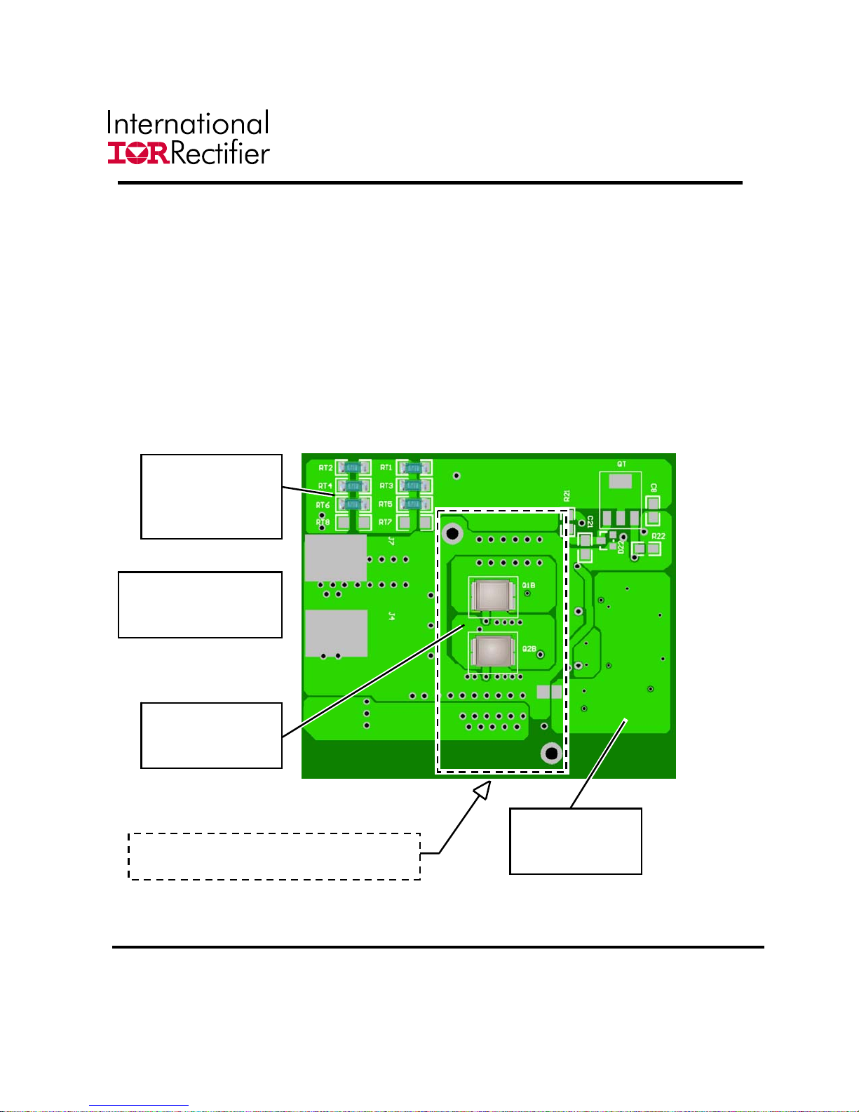
CIRCUIT LAYOUT- BOTTOM LAYER
Solder pads for off-board connections ground are
available on the bottom layer. A portion of the
bottom layer plane is isolated for use as Signal
Ground. Options for making the required single
point of connection between Signal ground and
Power Ground are provided on the top side of the
board.
MX-packaged DirectFets can be mounted on the
bottom side of the board. The bottom–side location
of the DirectFet packages allows convenient
attachment of a heat sink.
Low Voltage
Linear Regulator
Components
IRDC3651
The IR3651 controller requires a low voltage
power source (nominally 12V). Elements of a
simple linear voltage regulator are installed on
a circuit pattern provided on the bottom layer to
generate the required voltage from the 48V
input supply.
Alternatively, a separate external 12V supply
can be connected at J12, on the top side of the
board.
Off - board Ground
Connection Pads
DirectFet
Positions
Heat Sink mounting area (optional)
Figure 3 – Bottom layer of the IR3651 evaluation board.
Rev 1.1
12/20/2006
RD-0616
Signal Ground
Plane
4
Page 5
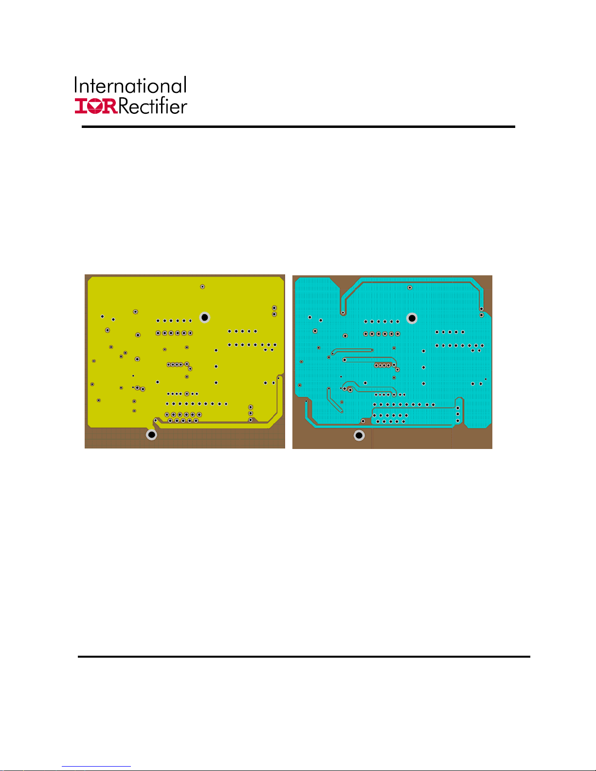
LAYOUT -- MID-LAYERS
The two mid-layers are used primarily for Power
Ground.
IRDC3651
Mid-layer 1 Mid-layer 2
Figure 3 – Internal layers of IR3651 evaluation board.
Rev 1.1
12/20/2006
RD-0616
5
Page 6

IRDC3651
Rev 1.1
12/20/2006
RD-0616
Figure 4 – Schematic of the IR3651 evaluation board
6
Page 7

IRDC3651
BILL OF MATERIALS
Quantity Designator Val ue 1 Va lu e 2 Tolerance Description 1 Description 2 Packa ge Source Source Pa rt No.
1 U1 * * * IC PWM Cont r o ller SO IC - 1 4 IR IR365 1
1 Q1B * * * MOS F E T POWE R NF E T Direc t F ET IR IRF6662
1 Q2B * * * MOS F E T POWE R NF E T Direc t F ET IR IRF6646
1 D1 * * * DIODE S i l icon PN SOT-23 ON MMBD6100LT1
1 D23 12V 230mW * Zener Diode * SOT-23 Diodes Inc. B ZX84C12-7-F
1 ROCSet 19.1k 1/8W 1% RES IS TOR thi ck fil m 0805 Panas oni c-ECG ERJ-6ENF1912V
RT1, RT2,
6
RT3, RT4,
RT5, RT6
3 R6, 10, 20 0 Ohm 1/8W 1% RESISTOR thick film 0805 P anas onic -E CG E RJ-6ENF0R00V
1 R11 665 Ohm 1/8W 1% RESISTOR thick film 0805 Panas onic-ECG ERJ-6ENF6650V
1 R3 1.5k 1/8W 1% RE S IS TOR thi ck fil m 0805 Panas oni c-ECG E RJ-6E NF 1501V
1 R4 4.99k 1/8W 1% RESIS TOR thi ck fil m 0805 Panas oni c-ECG E RJ-6E NF 4991V
1 R2 17.4k 1/8W 1% RESIS TOR thi ck fil m 0805 Panas on ic-ECG E RJ-6E NF 1742V
1 R1 28.7k 1/8W 1% RESIS TOR thi ck fil m 0805 Panas on ic-ECG E RJ-6E NF 2872V
1 R5 255k 1/8W 1% RESIS TOR thi c k film 0805 Panasonic-ECG E RJ-6E NF25 53V
1 C10 220pF 50V 5% CAP A CITOR C0G (NP0) 0805 KEMET C0805C221J5GACTU
1 C9 2.2nF 50V 5% CAPACITOR C0G (NP0) 0805 MURA TA GRM2165C1H222 JA 01D
1 C7 18nF 50V 5% CA P A CITOR C0G (NP0) 0805 MURATA GRM21B5C1H183JA01L
2 C4, 6 0.1uF 25V 10% CAPACITOR X7R 0805 YA EGO CC0805K RX7R8BB104
2 C3, 5 1u F 16V 10% CAPACITOR X5R 0805 Panasonic-ECG E CJ-2FB1C105K
C1A , C1 B,
3
2 C8A, C8B 330uF 6V * CAP A CITOR POS CAP * SANY O 6TPD330M
1 L1 6.8uH * * INDUCTOR * 0.5 x 0.5 A CT STS1305-6R8M
1 Circui t board * * * PCB Rev_11 * IR DB513
5
2 RT7, RT8 UNUSED * * * * 1206 * *
4 C1, 2, 8, 21 UNUSED * * * * 0805 * *
3
1 C8C UNUSED * * * * * * *
5
1 D22 UNUSED * * * * SOT-23 * *
1 QT UNUSED * * * * SOT-223 * *
2 Q1A , Q 2A UNUSE D * * * * SO-8 * *
C1C
R7, 8, 9, 21,
22, 23
C1D, C1 E ,
C1F
C5A , C5 B,
C20A, C20B,
C20C
2.43k 1/4W 1% RES IS TOR thi ck fi l m 1206 Panas oni c-ECG ERJ-8ENF2431V
2.2uF 100V * CAPACITOR X7R 1210 MURATA GRM32ER72A225K
UNUSED * * * * 0805 * *
UNUSED * * * * 1210 * *
UNUSED * * * * 1210 * *
Rev 1.1
12/20/2006
RD-0616
db513_11-IR3651_48V-Buck-3.3V_Eval_Board_BOM_Rev1.42.xls
7
Page 8

TYPICAL Output WAVEFORMS
Vin=48V, Vo=3.3V, Room Temperature, No Air Flow
IRDC3651
0A load
10A load
Cyan: V
Blue: V
Green: I
IN
OUT
OUT
Rev 1.1
12/20/2006
Figure 5 – Startup waveforms
RD-0616
8
Page 9

TYPICAL Output WAVEFORMS
Vin=48V, Vo=3.3V, Room Temperature, No Air Flow
IRDC3651
Figure 6 – 0A to 10A Transient
Figure 7 – Output Ripple, 10A load
Blue: V
Green: I
OUT
OUT
Rev 1.1
12/20/2006
RD-0616
9
Page 10

TYPICAL Output WAVEFORMS
Vin=48V, Vo=3.3V, Room Temperature, No Air Flow
IRDC3651
Short Circuit :
Operation and Recovery
Short Circuit :
Detail of “Hiccup”
Figure 8 – Short Circuit Response
Blue: V
Green: I
OUT
OUT
Magenta: V
SS
Rev 1.1
12/20/2006
RD-0616
10
Page 11

TYPICAL Output WAVEFORMS
Vin=48V, Vo=3.3V, Room Temperature, No Air Flow
IRDC3651
0A Load
Figure 9 – Shutdown
Blue: V
Cyan: V
Green: I
Magenta: V
10A Load
OUT
IN
OUT
SS
Rev 1.1
12/20/2006
RD-0616
11
Page 12

TYPICAL Output WAVEFORMS
Vin=48V, Vo=3.3V, Room Temperature, No Air Flow
IRDC3651
Rev 1.1
12/20/2006
Figure 10 – Efficiency
RD-0616
12
Page 13

Vin=48V, Vo=3.3V, 10A Load, Room Temperature, No Air Flow
IRDC3651
(1) IR5651 Controller
(2) Inductor
(3) Output Capacitors
Figure 11a – Temperature Distribution, Top side
(1) IRF6646 Sync-Rectifier FET
(2) IRF6662 Switch FET
(3) 12V linear supply resistor
Figure 11b – Temperature Distribution, bottom side
Rev 1.1
12/20/2006
RD-0616
13
Page 14

Mouser Electronics
Authorized Distributor
Click to View Pricing, Inventory, Delivery & Lifecycle Information:
International Rectifier:
IRDC3651
 Loading...