

Page 1

IR3621 EV ALUA TION BOARD USER GUIDE
Dual output using MOSFET s in SO8 package
IRDC3621EVAL
INTRODUCTION
DESCRIPTION
The IR3621 IC combines a Dual synchronous Buck controller, providing a cost-ef fective, high performance and
flexible solution. The IR3621 can be configured in 2-independent output or as a 2-phase mode. The 2-phase
configuration is ideal for high current applications. The
IR3621 features 180 out of phase operation which reduces the required input/output capacitance. Other key
features offered by this device include two independent
programmable soft starts, PreBias start up, programmable switching frequency up to 500KHz per phase,
external frequency synchronization and under voltage
lockout for proper start up. The current limit is provided
by sensing the lower MOSFET's on-resistance for optimum cost and performance.
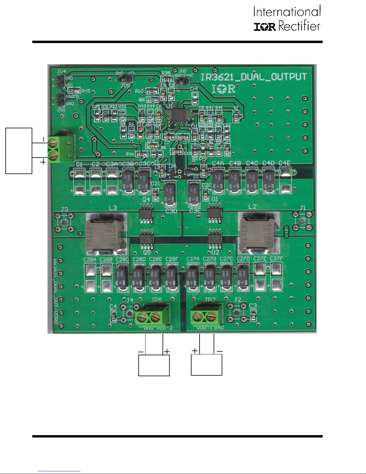
INPUT/OUTPUT CONNECTIONS
The following is the input/output connections:
Inputs:
JP1: Vin and Gnd
JU4: VCC and Gnd
JU5: VCL
Outputs:
JP2: Vout1
JP5: Vout2
Scope Probe connections:
J1 and J3: Inductor point for L2 and L3
J2 and J4: Outputs for V out1 and Vout2
SPECIFICATION DATA
This reference board is designed for Dual output
configuration and will demonstrate the main features of
IC.
This user guide contains the schematic and bill of
materials, the design guidelines are described in data
sheet.
The connection points for dual output application are
shown in Figure 1. Connect the power supply cables
according to this figure, minimizing wire lengths to reduce losses in the wire. Test points J1, J2, J3 and J4
provide easy connection for oscilloscope voltage probe
to monitor the inductor points for each PWM section
and output voltages.
Application Data:
VIN = 12V
VOUT1 = 2.5V
IOUT1 = 10A
VOUT2 = 1.8V
IOUT2 = 10A
∆VOUT = 50mV
FS = 400KHz
PGOOD: JU1
SYNC: JU2
Rev.1.0
Dual_output_2xSO8
6/7/2005
www.irf.com
1
Page 2
IRDC3621EVAL
CONNECTION DIAGRAM
Power Supply
12V
Figure 1 - Connection diagram of evaluation-board
2
LOAD
0-10A
www.irf.com
LOAD
0-10A
Rev.1.0
Dual_output_2xSO8
6/7/2005
Page 3
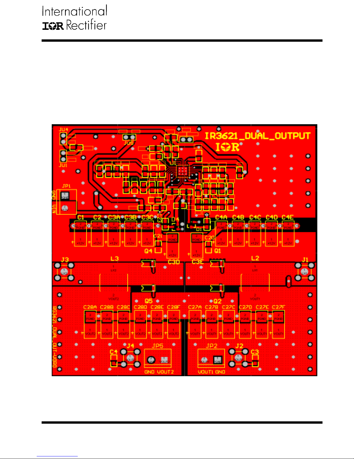
LAYOUT
The PCB is 4-layers FR4 board, the top layer is dedicated for power components, with control MOSFET s and
Synchronous MOSFET s. These MOSFETs are SOIC-8
footprint. The input capacitors are all located close to
MOSFET s. The two output inductors are located closed
to MOSFETs.
The two mid-layers are dedicated for Analog and Power
ground, these two grounds are kept separated from each
other and they are connected at a single point as shown
in Figure3.
IRDC3621EVAL
All the decoupling capacitors, charge pump capacitor
and feedback components are located close to the IC.
The feedback resistors are tied to the output voltage at
the point of regulation and are located close to the IC.
Rev.1.0
Dual_output_2xSO8
6/7/2005
Figure 2 - T op layer of evaluation-board
www.irf.com
3
Page 4

IRDC3621EVAL
Figure 3 - Mid layer of evaluation-board
4
www.irf.com
Dual_output_2xSO8
Rev.1.0
6/7/2005
Page 5

IRDC3621EVAL
Rev.1.0
Dual_output_2xSO8
6/7/2005
Figure 4 - Schematic of the evaluation Board
www.irf.com
5
Page 6

IRDC3621EVAL
BILL OF MATERIAL For Dual Output Application, Vin=12V,
Vout1=2.5V@10A, Vout2=1.8V@10A, Fs=400KHz
Ref Desig Description Value Qty Part# Manuf
Q1,Q4
Q2,Q5
U1
D1,D4
D2,D3
L2,L3
C3B-D, C4A-E
C27A-D, C28C-F
C14,C15,C16,C17,C18,C23
C3,C4,C5,C6,C7,C8,C9,C20,C21
C13
C11
R2
R5
R8
R12,R19
R27,R41
R29,R33,R42,R44
R31,R43
R45
R3,6,7,10,1 1,13,18,20,35,36
R1,4,9,32,
C1,2,C3A,C3E, C27E-F ,C28A-B,
C10,12,19,22,24,25,26
J1,J2,J3,J4
JP1,JP2,JP5
JU1,JU2,JU4,JU5
MOSFET
MOSFET
Controller
Diode
Diode
Inductor
Cap,Poscap
Cap,Poscap
Cap,Ceramic
Cap,Ceramic
Cap,Ceramic
Cap,Ceramic
Resistor
Resistor
Resistor
Resistor
Resistor
Resistor
Resistor
Resistor
Resistor
Resistor
Capacitor
Capacitor
Scope Probe
Terminal
Jumper
30V ,11mOhm
30V , 6mOhm
Synchronous PWM
Fast Switching
Fast Switching
1.1µH,16A
47µF , 16V ,70mΩ
330µF,6.3V,40mΩ
0.1µF, Y5V, 25V
1µF, Y5V, 16V
10nF , X7R, 50V
8.2nF,X7R,50V
6.2K
4.7K
22.6K
5.1 1K, 1%
2.15K, 1%
1K, 1%
1.24K,1%
49.9K,1%
Short, 0Ω
Open
Open
Open
2-Pos terminal
2
IRF7821
2
IRF81 13
1
IR3621M
2
BA T54S
2
BAT54A
2
ETQP6F1R1BFA
8
16TPB47M
8
6TPB330M
6
ECJ-2VF1E104Z
9
ECJ-2VF1C105Z
1
ECJ-2VB1H103K
1
ECJ-2VB1H822K
1
Any
1
1
2
2
4
2
1
10
4
8
7
4
131-5031-00
3
ED1973-ND
S1012-02-ND
4
IR
IR
IR
IR
IR
Panasonic
Sanyo
Sanyo
Panasonic
Panasonic
Panasonic
Panasonic
Tektronix
Digi-Key
Digi-Key
6
www.irf.com
Dual_output_2xSO8
Rev.1.0
6/7/2005
Page 7

IRDC3621EVAL
TYPICAL OPERA TING W aveforms
T est Conditions:
VIN=12V , VOUT1=2.5V, IOUT1=0-10A, VOUT2=1.8V , IOUT2=0-10A, Fs=400KHz, TA=Room Temp, No Air Flow
Unless otherwise specified.
Figure 5 - St art up wavforms for 2.5V output
Ch1: Vin, Ch2: V out3, Ch3: SS1, Ch4:V o1 (2.5V)
Figure 7 - Start up wavforms
Ch1: Vin, Ch2: V out3, Ch3: V ref
Figure 6 - Start up wavforms for 1.8V output
Ch1: Vin, Ch2: V out3, Ch3: SS2, Ch4:V o2 (1.8V)
Figure 8 - Vo1, V o2 and PGood
Ch1: Vin, Ch2: V o1, Ch3: V o2, Ch4: PGood
Rev.1.0
Dual_output_2xSO8
6/7/2005
www.irf.com
7
Page 8

IRDC3621EVAL
TYPICAL OPERA TING W aveforms
T est Conditions:
VIN=12V, VOUT1=2.5V, IOUT1=0-10A, VOUT2=1.8V, IOUT2=0-10A, Fs=400KHz, Ta=Room Temp, No Air Flow
Unless otherwise specified.
Figure 9 - 2.5V output
Ch1: Vin, Ch2: SS1, Ch3: V o1, Ch4: PGood
Figure1 1 - Gate waveforms with 180
out of phase
Ch1: Hdrv1, Ch2: Hdrv2
o
Figure 10 - 1.8V output
Ch1: Vin, Ch2: SS2, Ch3: V o2, Ch4: PGood
Figure 12 - 2.5V Waveforms
Ch1: Hdrv1, Ch2: Ldrv1, Ch3: Lx1, Ch4: Inductor Current
8
www.irf.com
Dual_output_2xSO8
Rev.1.0
6/7/2005
Page 9

IRDC3621EVAL
TYPICAL OPERA TING W aveforms
T est Conditions:
VIN=12V, VOUT1=2.5V, IOUT1=0-10A, VOUT2=1.8V, IOUT2=0-10A, Fs=400KHz, Ta=Room Temp, No Air Flow
Unless otherwise specified.
Figure 13 - 2.5V Waveforms
Ch1: Hdrv2, Ch2: Ldrv2, Ch3: Lx2, Ch4: Inductor Current
Figure 15 - 2.5V output shorted
Ch1: Vo2, Ch2: SS1, Ch3: Inductor Current
Figure14 - 1.8V output shorted
Ch1: Vo1, Ch2: SS2, Ch3: Inductor Current
Figure 16 - Prebias Start up
Ch1: SS1, Ch2: Vo1, Ch3: SS2, Ch4:V o2
Rev.1.0
Dual_output_2xSO8
6/7/2005
www.irf.com
9
Page 10

IRDC3621EVAL
TYPICAL OPERA TING W aveforms
T est Conditions:
VIN=12V, VOUT1=2.5V, IOUT1=0-10A, VOUT2=1.8V, IOUT2=0-10A, Fs=400KHz, Ta=Room Temp, No Air Flow
Unless otherwise specified.
Figure 17 - SS1 pin shorted to Gnd
Ch1: SS1, Ch2: Hdrv1, Ch3: Ldrv1, Ch4:Vo2
Figure 18 - SS2 pin shorted to Gnd
Ch1: SS2, Ch2: Hdrv2, Ch3: Ldrv2, Ch4:Vo1
Ch1: Extrnal Clocl, Ch2: Hdrv1, Ch3: Hdrv2
10
Figure 19 - Extrnal Synchronization
www.irf.com
Dual_output_2xSO8
Rev.1.0
6/7/2005
Page 11

IRDC3621EVAL
TYPICAL OPERA TING W aveforms
T est Conditions:
VIN=12V, VOUT1=2.5V, IOUT1=0-10A, VOUT2=1.8V, IOUT2=0-10A, Fs=400KHz, Ta=Room Temp, No Air Flow
Unless otherwise specified.
Figure 20 - Load Transient Respons for V o1
(Io=0 to 10A)
Ch1: Vo1, Ch4: Io1
Figure 22 - Load Transient Respons for V o2
(Io=0 to 10A)
Ch1: Vo2, Ch4: Io2
Figure 21 - Load Transient Respons for V o1
(Io=10 to 0A)
Ch1: Vo1, Ch4: Io1
Figure 23 - Load Transient Respons for V o2
(Io=10 to 0A)
Ch1: Vo2, Ch4: Io2
Rev.1.0
Dual_output_2xSO8
6/7/2005
www.irf.com
11
Page 12

IRDC3621EVAL
TYPICAL PERFORMANCE CURVES
12V to 2.5V and 1.8V
90
85
80
75
70
65
Efficien cy (%)
60
55
50
45
0 2 4 6 8 10 12 14 16
Io(A)
Figure 24- Efficiency for 2.5V and 1.8V outputs at room temperature no air flow .
When measuring one output, the other output was running at no load.
2.5V
1.8V
12
www.irf.com
Dual_output_2xSO8
Rev.1.0
6/7/2005
Page 13

IRDC3621EVAL
Figure 25- Thermal Images for Both Outputs at Vin:12V, Vout1:2.5V @ 10A, V out2:1.8V
@ 10A. Room T emperature, No Air Flow
Test Point: 1) Sync FET for 2.5V output
2)Sync FET for 1.8V output
3) IR3621M IC.
Rev.1.0
Dual_output_2xSO8
6/7/2005
www.irf.com
13
 Loading...