

Page 1
Data Sheet No. PD60173-E
IR2183(4
) (S)
HALF-BRIDGE DRIVER
Features
Floating channel designed for bootstrap operation
•
Fully operational to +600V
Tolerant to negative transient voltage
dV/dt immune
Gate drive supply range from 10 to 20V
•
Undervoltage lockout for both channels
•
3.3V and 5V input logic compatible
•
Matched propagation delay for both channels
•
Logic and power ground +/- 5V offset.
•
Lower di/dt gate driver for better noise immunity
•
Output source/sink current capability 1.4A/1.8A
•
Description
The IR2183(4)(S) are high voltage,
high speed power MOSFET and IGBT
drivers with dependent high and low
side referenced output channels. Proprietary HVIC and latch immune
CMOS technologies enable ruggedized monolithic construction. The
logic input is compatible with standard
CMOS or LSTTL output, down to 3.3V
logic. The output drivers feature a high
pulse current buffer stage designed for minimum driver cross-conduction. The floating channel can be used to
drive an N-channel power MOSFET or IGBT in the high side configuration which operates up to 600 volts.
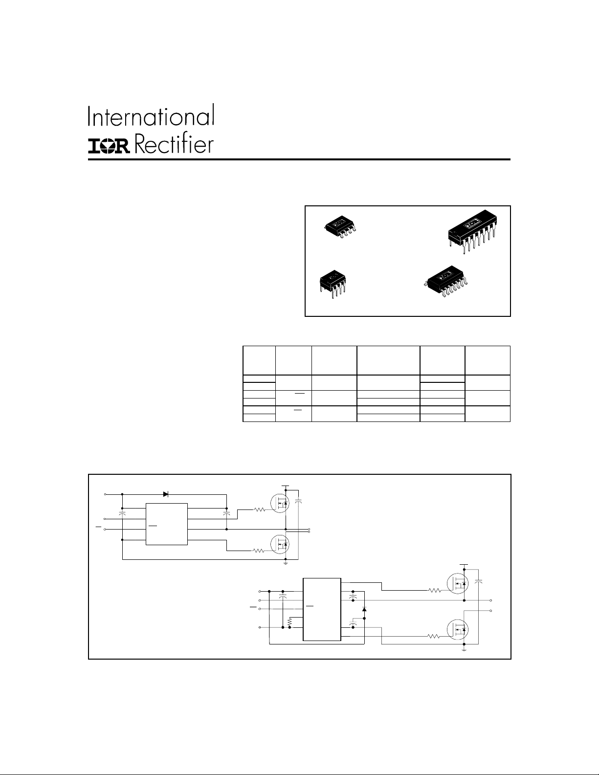
IR2181/IR2183/IR2184 Feature Comparison
Part
2181 COM
21814
2183 Internal 500ns COM
21834
2184 Internal 500ns COM
21844
Packages
8-Lead SOIC
IR2183S
8-Lead PDIP
IR2183
Input
logic
HIN/LIN no none
HIN/LIN yes
IN/SD yes
Crossconduction
prevention
logic
Dead-Time Ground Pins Ton/Toff
Program 0.4 ~ 5 us VSS/COM
Program 0.4 ~ 5 us VSS/COM
14-Lead PDIP
IR21834
VSS/COM
14-Lead SOIC
IR21834S
180/220 n s
180/220 n s
680/270 n s
T ypical Connection
up to 600V
V
CC
HIN
LIN
(Refer to Lead Assignment for correct pin
configuration) This/These diagram(s) show
electrical connections only. Please refer to our
Application Notes and DesignTips for proper circuit
board layout.
V
HIN
LIN
www.irf.com 1
V
CC
B
HO
V
S
LOCOM
IR2183
V
HIN
V
TO
LOAD
up to 600V
HO
V
V
CC
CC
LIN
SS
HIN
LIN
DT
V
R
DT
B
V
S
COM
SS
LO
IR21834
TO
LOAD
Page 2
IR2183(4
) (S)
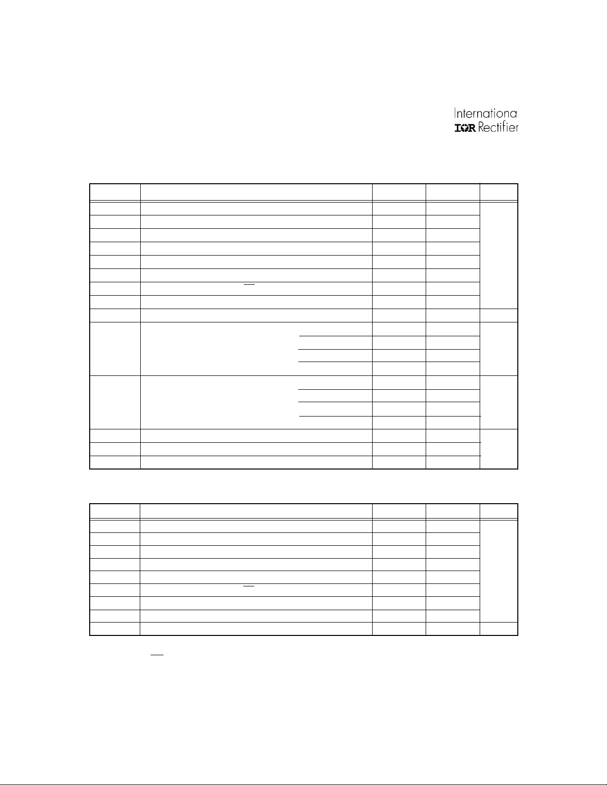
Absolute Maximum Ratings
Absolute maximum ratings indicate sustained limits beyond which damage to the device may occur. All voltage parameters are absolute voltages referenced to COM. The thermal resistance and power dissipation ratings are measured
under board mounted and still air conditions.
Symbol Definition Min. Max. Units
V
B
V
S
V
HO
V
CC
V
LO
DT Programmable dead-time pin voltage (IR21834 only) VSS - 0.3 V
V
IN
V
SS
dVS/dt Allowable offset supply voltage transient — 50 V/ns
P
D
Rth
JA
T
J
T
S
T
L
High side floating absolute voltage -0.3 625
High side floating supply offset voltage VB - 25 VB + 0.3
High side floating output voltage VS - 0.3 V
+ 0.3
B
Low side and logic fixed supply voltage -0.3 25
Low side output voltage -0.3 VCC + 0.3
+ 0.3
CC
Logic input voltage (HIN &
Logic ground (IR21834 only) V
)V
LIN
- 0.3 V
SS
- 25 V
CC
SS
CC
+ 10
+ 0.3
Package power dissipation @ TA ≤ +25°C (8-lead PDIP) — 1.0
(8-lead SOIC) — 0.625
(14-lead PDIP) — 1.6
(14-lead SOIC) — 1.0
Thermal resistance, junction to ambient (8-lead PDIP) — 125
(8-lead SOIC) — 200
(14-lead PDIP) — 75
(14-lead SOIC) — 120
Junction temperature — 150
Storage temperature -50 150
Lead temperature (soldering, 10 seconds) — 300
V
W
°C/W
°C
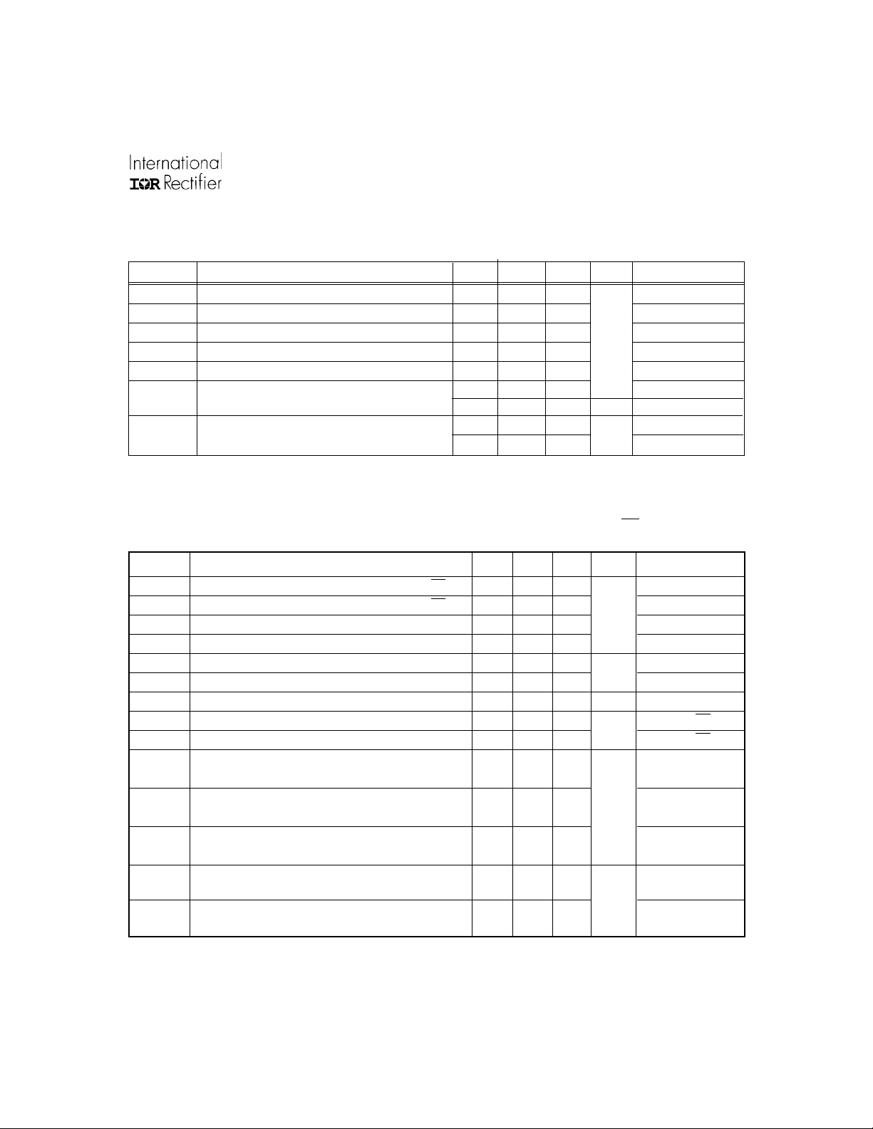
Recommended Operating Conditions
The Input/Output logic timing diagram is shown in figure 1. For proper operation the device should be used within the
recommended conditions. The VS and VSS offset rating are tested with all supplies biased at 15V differential.
Symbol Definition Min. Max. Units
VB High side floating supply absolute voltage VS + 10 VS + 20
V
S
V
HO
V
CC
V
LO
V
IN
DT Programmable dead-time pin voltage (IR21834 only) V
V
SS
T
A
Note 1: Logic operational for VS of -5 to +600V. Logic state held for VS of -5V to -VBS. (Please refer to the Design Tip
DT97-3 for more details).
Note 2: HIN and LIN pins are internally clamped with a 5.2V zener diode.
High side floating supply offset voltage Note 1 600
High side floating output voltage V
S
V
B
Low side and logic fixed supply voltage 10 20
Low side output voltage 0 V
Logic input voltage (HIN &
)V
LIN
SS
SS
CC
V
+ 5
SS
V
CC
Logic ground (IR21834 only) -5 5
Ambient temperature -40 125 °C
V
2 www.irf.com
Page 3
IR2183(4
) (S)
Dynamic Electrical Characteristics
V
(VCC, VBS) = 15V, VSS = COM, CL = 1000 pF, TA = 25°C, DT = VSS unless otherwise specified.
BIAS
Symbol Definition Min. Typ. Max. Units Test Conditions
t
on
t
off
MT Delay matching | ton - t
t
t
DT Deadtime: LO turn-off to HO turn-on(DT
MDT Deadtime matching = | DT
Turn-on propagation delay — 180 270 VS = 0V
Turn-off propagation delay — 220 330 VS = 0V or 600V
off
|
Turn-on rise time — 40 60 VS = 0V
r
Turn-off fall time — 20 35 VS = 0V
f
LO-HO) &
HO turn-off to LO turn-on (DT
LO-HO
- DT
HO-LO)
HO-LO
— 035
280 400 520 RDT= 0
456µsec RDT = 200k (IR21834)
— 0 50 RDT=0
|
— 0 600 RDT = 200k (IR21834)
nsec
nsec
Static Electrical Characteristics
V
(VCC, VBS) = 15V, VSS = COM, DT= VSS and TA = 25°C unless otherwise specified. The VIL, VIH and I
BIAS
parameters are referenced to VSS/COM and are applicable to the respective input leads: HIN and LIN. The VO, IO and Ron
parameters are referenced to COM and are applicable to the respective output leads: HO and LO.
Symbol Definition Min. Typ. Max. Units T est Conditions
V
IH
V
V
OH
V
OL
I
LK
I
QBS
I
QCC
I
IN+
I
IN-
V
CCUV+VCC
V
BSUV+
V
CCUV-
V
BSUV-
V
CCUVH
V
BSUVH
I
O+
I
O-
Logic “1” input voltage for HIN & logic “0” for
Logic “0” input voltage for HIN & logic “1” for
IL
High level output voltage, V
Low level output voltage, V
Offset supply leakage current ——50 VB = VS = 600V
Quiescent VBS supply current 20 60 150 V
Quiescent VCC supply current 0.4 1.0 1.6 mA VIN = 0V or 5V
Logic “1” input bias current — 5 20 HIN = 5V,
Logic “0” input bias current — 1 2 HIN = 0V,
and VBS supply undervoltage positive going 8.0 8.9 9.8
threshold
VCC and V
threshold
Hysteresis 0.3 0.7 —
Output high short circuit pulsed current 1.4 1.9 — VO = 0V,
Output low short circuit pulsed current 1.8 2.3 — VO = 15V,
supply undervoltage negative going 7.4 8.2 9.0
BS
BIAS
O
- V
O
LIN
LIN
2.7 —— VCC = 10V to 20V
——0.8 VCC = 10V to 20V
——1.2 IO = 0A
——0.1 IO = 0A
V
µA
µA
V
A
IN
= 0V or 5V
IN
LIN
LIN
PW ≤ 10 µs
PW ≤ 10 µs
= 0V
= 5V
www.irf.com 3
Page 4

IR2183(4
) (S)
Functional Block Diagrams
2183
HIN
VSS/COM
LEVEL
SHIFT
PULSE
GENERATOR
HV
LEVEL
SHIFTER
PULSE
FILTER
UV
DETECT
VB
R
Q
R
S
HO
VS
LIN
HIN
DT
LIN
DT
+5V
VSS
+5V
DEADTIME &
SHOOT-THROUGH
PREVENTION
21834
DEADTIME &
SHOOT-THROUGH
PREVENTION
VSS/COM
LEVEL
SHIFT
VSS/COM
LEVEL
SHIFT
VSS/COM
LEVEL
SHIFT
DELAY
PULSE
GENERATOR
DELAY
HV
LEVEL
SHIFTER
PULSE
FILTER
UV
DETECT
UV
DETECT
UV
DETECT
VCC
LO
COM
VB
R
Q
R
S
HO
VS
VCC
LO
COM
VSS
4 www.irf.com
Page 5

IR2183(4
) (S)
Lead Definitions
Symbol Description
HIN Logic input for high side gate driver output (HO), in phase (referenced to COM for IR2183 and
VSS for IR21834)
LIN
DT Programmable dead-time lead, referenced to VSS. (IR21834 only)
VSS Logic Ground (21834 only)
V
B
HO High side gate driver output
V
S
V
CC
LO Low side gate driver output
COM L ow side return
Logic input for low side gate driver output (LO), out of phase (referenced to COM for IR2183
and VSS for IR21834)
High side floating supply
High side floating supply return
Low side and logic fixed supply
Lead Assignments
HIN
1
LIN
2
COM
3
LO
4
V
8
B
HO
7
V
6
S
V
5
CC
HIN
1
LIN
2
COM
3
LO
4
8-Lead PDIP 8-Lead SOIC
IR2183 IR2183S
V
HO
V
14
13
B
12
11
S
10
9
8
HIN
1
LIN
2
VSS
3
DT
4
COM
5
LO
6
V
7
CC
14-Lead PDIP 14-Lead SOIC
HIN
1
LIN
2
VSS
3
DT
4
COM
5
LO
6
V
7
CC
IR21834 IR21834S
V
8
B
HO
7
V
6
S
V
5
CC
14
V
13
B
HO
12
V
11
S
10
9
8
www.irf.com 5
Page 6

IR2183(4
) (S)
Case outlines
A
87
6
E
e
6X
8X b
0.25 [.010] C A B
NOTES :
1. DIMENSIONING & TOLERANCING PER ASME Y14.5M-1994.
2. CONTROLLING DIMENSION: MILLIMETER
3. DIMENS IONS ARE SHOWN IN MILL IMET E RS [INCHES].
4. OUTLINE CONFORMS TO JEDEC OUTLINE MS-012AA.
D B
5
65
4312
e1
A1
H
0.25 [.010] A
A
C
0.10 [.004]
8-Lead PDIP
6.46 [.255]
3X 1.27 [.050]
y
8-Lead SOIC
01-3003 01
DIM
FOOTPRINT
8X 0.72 [.028]
8X 1.78 [.070]
MIN MA X
.0688
.0532
A
A1
b
c .0075 .0098 0.19 0.25
D
E
e
e1
H
K
L
y
.0098
.0040
.020
.013
.1968
.189
.1574
.1497
.050 BASIC
.025 BASIC 0.635 BASIC
.2440
.2284
.0196
.0099
.050
.016
8°
0°
K x 45°
8X L
8X c
7
5 DIMENS ION DOES NOT INCLUDE MOLD PR OTRUS IONS.
MOLD PROTRUSIONS NOT TO EXCEED 0.15 [.006].
6 DIMENS ION DOES NOT INCLUDE MOLD PR OTRUS IONS.
MOLD PROTRUSIONS NOT TO EXCEED 0.25 [.010].
7 DIMENSION IS THE LENGTH OF LEAD FO R SOLD ERING TO
A SUBS TRATE.
01-0021 11
01-6014
(MS-001AB)
MILLIMETERSINCHES
MIN MA X
1.75
1.35
0.25
0.10
0.51
0.33
5.00
4.80
4.00
3.80
1.27 BASIC
6.20
5.80
0.50
0.25
1.27
0.40
0°
8°
01-6027
(MS-012AA)
6 www.irf.com
Page 7

14-Lead PDIP
IR2183(4
01-3002 03
) (S)
01-6010
(MS-001AC)
14-Lead SOIC (narrow body)
www.irf.com 7
01-3063 00
01-6019
(MS-012AB)
Page 8

IR2183(4
) (S)
HIN
LIN
HO
LO
Figure 1. Input/Output Timing Diagram
HIN
LIN
50% 50%
LIN
50%
t
off
90% 90%
50%
LO
50%
t
on
t
r
10% 10%
50%
HIN
t
on
t
r
90% 90%
HO
10% 10%
Figure 2. Switching Time Waveform Definitions
t
off
t
f
t
f
90%
HO
LO
DT
MDT=
LO-HO
90%
DT
10%
LO-HO
- DT
DT
HO-LO
HO-LO
10%
Figure 3. Deadtime Waveform Definitions
IR WORLD HEADQUARTERS: 233 Kansas St., El Segundo, California 90245 Tel: (310) 252-7105
Data and specifications subject to change without notice. 7/23/2001
8 www.irf.com
 Loading...