International Rectifier CPV 364 M 4 KPbF Service Manual

www.DataSheet4U.com
CPV364M4KPbF
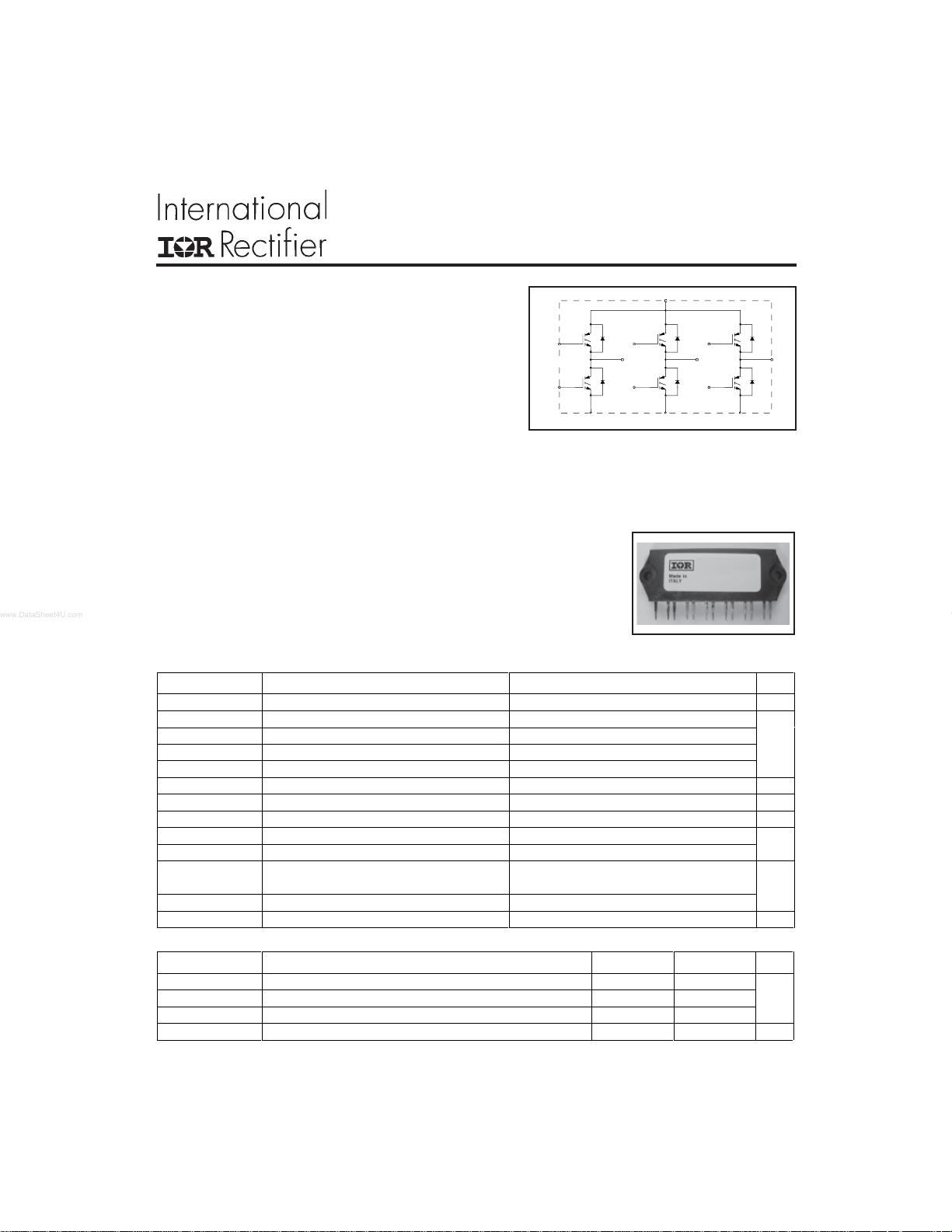
IGBT SIP MODULE
Features
• Short Circuit Rated UltraFast: Optimized for high
operating frequencies >5.0 kHz , and Short Circuit
Rated to 10μs @ 125°C, V
• Fully isolated printed circuit board mount package
• Switching-loss rating includes all "tail" losses
• HEXFRED
TM
soft ultrafast diodes
• Optimized for high operating frequency (over 5kHz)
• Totally Lead-Free and RoHs Compliant
Product Summary
Output Current in a Typical 20 kHz Motor Drive
11 A
per phase (3.1 kW total) with TC = 90°C, TJ = 125°C, Supply Voltage 360Vdc,
RMS
Power Factor 0.8, Modulation Depth 115% (See Figure 1)
Description
The IGBT technology is the key to International Rectifier's advanced line of
IMS (Isolated Metal Substrate) Power Modules. These modules are more
efficient than comparable bipolar transistor modules, while at the same time
having the simpler gate-drive requirements of the familiar power MOSFET.
This superior technology has now been coupled to a state of the art materials
system that maximizes power throughput with low thermal resistance. This
package is highly suited to motor drive applications and where space is at
a premium.
Absolute Maximum Ratings
GE
= 15V
Short Circuit Rated UltraFast IGBT
Q1
3
Q2
6
Bulletin I-27256 09/06
1
D1 D3 D5
Q3
9
D2 D4 D6
Q4
12
71319
Q5
15
10 164
Q6
18
Parameter Max. Units
V
CES
I
@ TC = 25°C Continuous Collector Current 24
C
I
@ TC = 100°C Continuous Collector Current 13 A
C
I
CM
I
LM
t
sc
V
GE
V
ISOL
Collector-to-Emitter Voltage 600 V
Pulsed Collector Current c 48
Clamped Inductive Load Current d 48
Short Circuit Withstand Time 9.3 μs
Gate-to-Emitter Voltage ±20 V
Isolation Voltage, any terminal to case, 1 min 2500 V
RMS
PD @ TC = 25°C Maximum Power Dissipation, each IGBT 63 W
P
@ TC = 100°C Maximum Power Dissipation, each IGBT 25
D
T
J
T
STG
Operating Junction and -55 to +150
Storage Temperature Range °C
Soldering Temperature, for 10 sec. 300 (0.063 in. (1.6mm) from case)
Mounting torque, 6-32 or M3 screw. 5-7 lbf•in ( 0.55-0.8 N•m)
Thermal Resistance
Parameter Typ. Max. Units
R
(IGBT) Junction-to-Case, each IGBT, one IGBT in conduction ––– 2.2
θJC
R
(DIODE) Junction-to-Case, each diode, one diode in conduction ––– 3.7 °C/W
θJC
R
(MODULE) Case-to-Sink, flat, greased surface 0.10 –––
θCS
Wt Weight of module 20 (0.7) ––– g (oz)
www.irf.com 1

CPV364M4KPbF
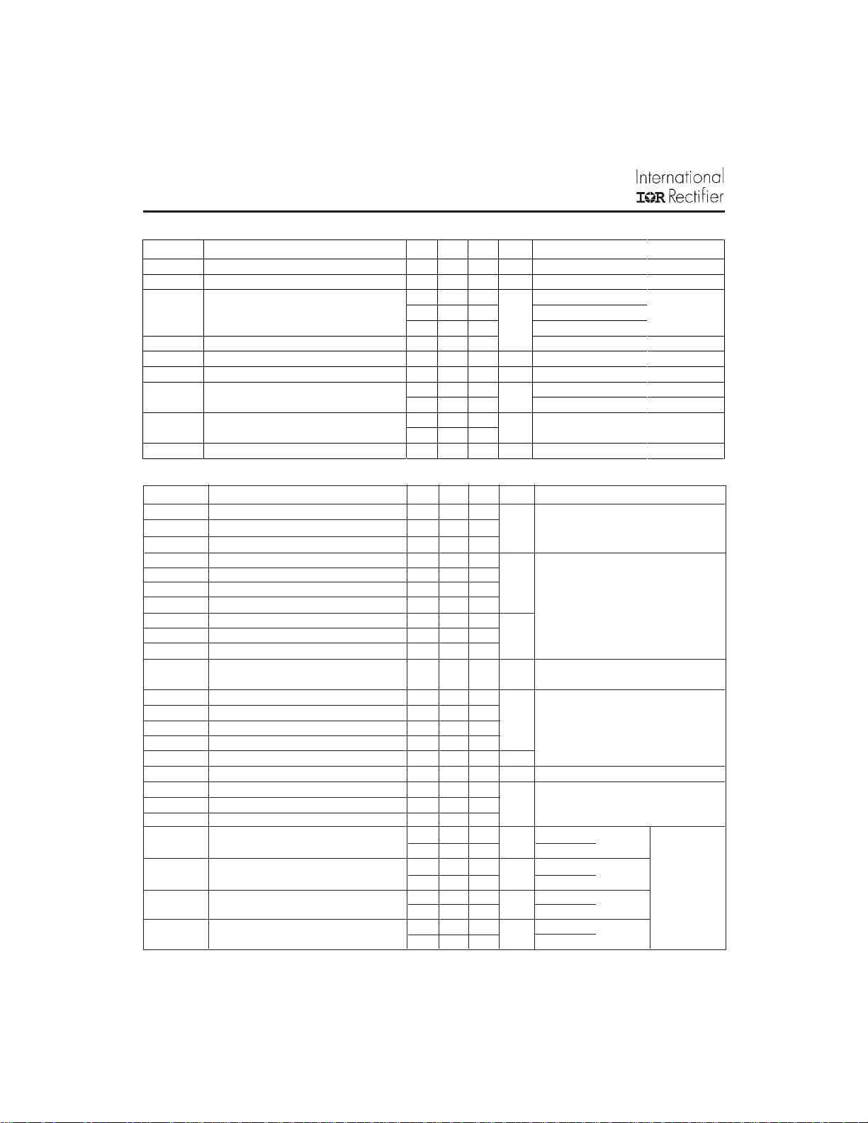
Electrical Characteristics @ T
= 25°C (unless otherwise specified)
J
Parameter Min. Typ. Max. Units Conditions
V
(BR)CES
ΔV
(BR)CES
V
CE(on)
V
GE(th)
ΔV
GE(th)
g
fe
I
CES
V
FM
I
GES
Collector-to-Emitter Breakdown Voltagee 600 ––– ––– V VGE = 0V, IC = 250μA
/ΔT
Temperature Coeff. of Breakdown Voltage ––– 0.63 ––– V/°C VGE = 0V, IC = 1.0mA
J
Collector-to-Emitter Saturation Voltage ––– 1.80 2.3 IC = 13A VGE = 15V
––– 1.80 ––– V I
––– 1.56 1.73 I
= 24A See Fig. 2, 5
C
= 13A, TJ = 150°C
C
Gate Threshold Voltage 3.0 ––– 6.0 VCE = VGE, IC = 250μA
/ΔT
Temperature Coeff. of Threshold Voltage ––– -13 ––– mV/°C VCE = VGE, IC = 250μA
J
Forward Transconductance f 11 18 ––– S VCE = 100V, IC = 10A
Zero Gate Voltage Collector Current ––– ––– 250 μ AVGE = 0V, VCE = 600V
––– ––– 3500 V
= 0V, VCE = 600V, TJ = 150°C
GE
Diode Forward Voltage Drop ––– 1.3 1.7 V IC = 15A See Fig. 13
––– 1.2 1.6 I
= 15A, TJ = 150°C
C
Gate-to-Emitter Leakage Current ––– ––– ±100 n A VGE = ±20V
Switching Characteristics @ TJ = 25°C (unless otherwise specified)
Parameter Min. Typ. Max. Units Conditions
Q
Q
Q
t
d(on)
t
r
t
d(off)
t
f
E
E
E
t
sc
t
d(on)
t
r
t
d(off)
t
f
E
L
C
C
C
t
rr
I
rr
Q
di
g
ge
gc
on
off
ts
ts
E
ies
oes
res
rr
(rec)M
Total Gate Charge (turn-on) — 110 170 IC = 13A
Gate - Emitter Charge (turn-on) — 14 21 nC VCC = 400V See Fig.8
Gate - Collector Charge (turn-on) — 49 74 VGE = 15V
Turn-On Delay Time — 50 —
Rise Time — 30 — TJ = 25°C
Turn-Off Delay Time — 110 170 IC = 13A, VCC = 480V
ns
Fall Time — 91 140 VGE = 15V, RG = 10Ω
Turn-On Switching Loss — 0.56 — Energy losses include "tail"
Turn-Off Switching Loss — 0.28 — mJ and diode reverse recovery
Total Switching Loss — 0.84 1.1 See Fig. 9,10, 18
Short Circuit Withstand Time 10 — — μsVCC = 360V, TJ = 125°C
V
= 15V, RG = 10Ω , V
GE
Turn-On Delay Time — 47 — TJ = 150°C, See Fig. 11,18
Rise Time — 30 — IC = 13A, VCC = 480V
Turn-Off Delay Time — 250 — VGE = 15V, RG = 10Ω
ns
Fall Time — 150 — Energy losses include "tail"
Total Switching Loss — 1.28 — mJ and diode reverse recovery
Internal Emitter Inductance — 7.5 — nH Measured 5mm from package
Input Capacitance — 1600 — VGE = 0V
Output Capacitance — 130 — pF VCC = 30V See Fig. 7
Reverse Transfer Capacitance — 55 — ƒ = 1.0MHz
Diode Reverse Recovery Time — 42 60 ns TJ = 25°C See Fig.
— 74 120 T
= 125°C 14 IF = 15A
J
Diode Peak Reverse Recovery Current — 4.0 6.0 A TJ = 25°C See Fig.
— 6.5 10 T
= 125°C 15 VR = 200V
J
Diode Reverse Recovery Charge — 80 180 nC TJ = 25°C See Fig.
— 220 600 T
= 125°C 16 di/dt = 200Aμs
J
/dt Diode Peak Rate of Fall of Recovery — 188 — A/μsTJ = 25°C See Fig.
During t
b
— 160 — TJ = 125°C 17
2
< 500V
CPK
www.irf.com

CPV364M4KPbF
18
16
14
12
10
8
6
LOAD CURRENT (A)
4
2
0
0.1 1 10 100
Tc = 90°C
Tj = 125° C
Power Factor = 0.8
Modulation Depth = 1.15
Vcc = 50% of Rated Voltage
f, Frequency (KHz)
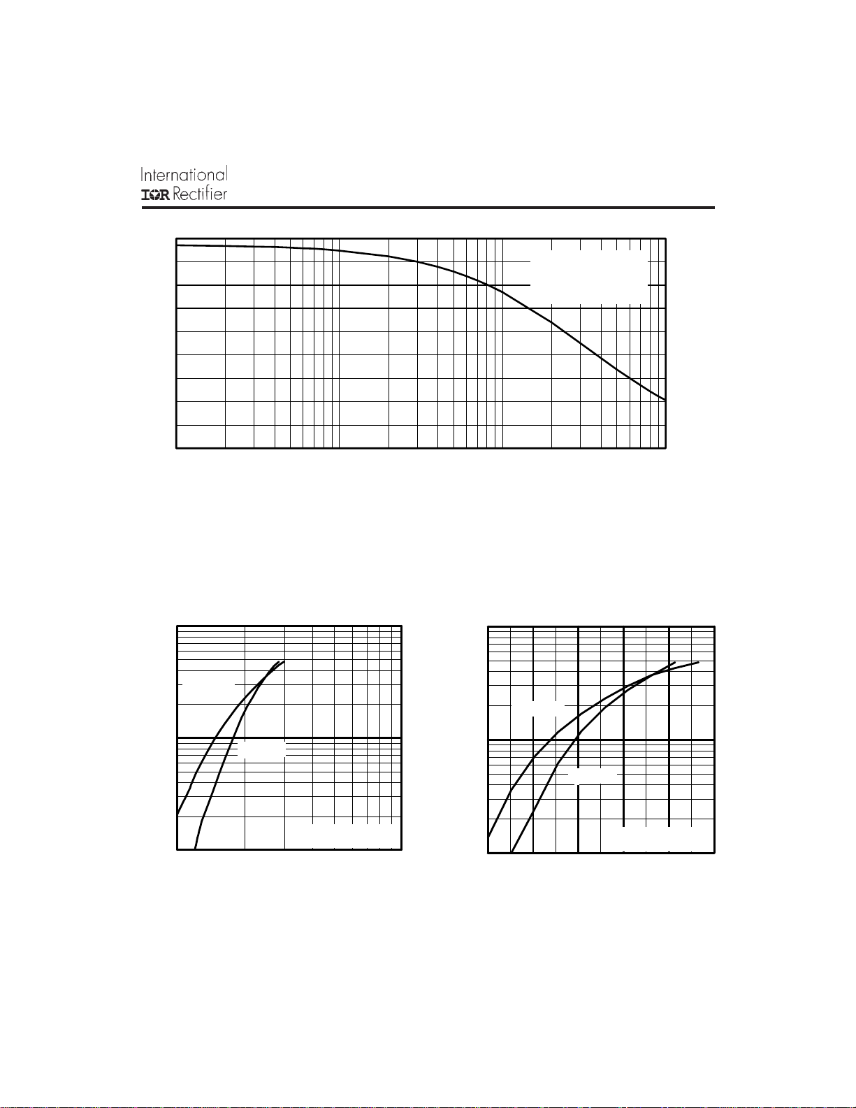
Fig. 1 - Typical Load Current vs. Frequency
(Load Current = I
100
of fundamental)
RMS
100
5.27
4.68
4.10
3.51
2.93
2.34
1.76
1.17
Total Output Power (kW)
0.59
0.00
°
T = 150 C
J
10
C
I , Collector-to-Emitter Current (A)
1
1 10
V , Collector-to-Emitter Voltage (V)
CE
T = 25 C
J
°
V = 15V
GE
20µs PULSE WIDTH
Fig. 2 - Typical Output Characteristics
°
T = 150 C
J
10
°
T = 25 C
J
C
I , Collector-to-Emitter Current (A)
1
5 6 7 8 9 10
V , Gate-to-Emitter Voltage (V)
GE
V = 50V
CC
5µs PULSE WIDTH
Fig. 3 - Typical Transfer Characteristics
3www.irf.com
 Loading...