

International Power Sources ZCA6C01PAPDI, ZCA6C01PAPDL, ZCA6C01PAPDM, ZCA6C16M, ZCA6C17I Datasheet
...
•
•
Input
AC Input Voltage • 85-264 VAC
Input Frequency • 47-63 Hz
DC Input Voltage • 48 VDC nominal (optional)
Power Factor • 0.99
Harmonic Current • Meets EN61000-3-2
Inrush Current • Limited to 30A peak
Input Protection • Internal 15A fuse
Output
Output Voltage • 1.8 VDC to 12 VDC
Output Power • 600W
Output Voltage Adj • ±5% min, See models chart
Minimum Load • 0 minimum load for all outputs
Line/Load Regulation • ±2% for V1, V2 and V3, ±3%
for V4 and V5
Ripple & Noise • >2.5V output: 50mV or 1% whichever
is greater <=2.5V output:
2% maximum
Transient Response • 4% max deviation, 300 µs recovery
time for a 25% load change
Temperature Co-eff. • 0.02%/°C
Hold Up Time • 20ms minimum
Remote Sense • Up to 0.25 V compensation on V1, V2
and V3
Overvoltage • V1, V2 and V3 only, recycle
Protection input to reset
Overcurrent • Standard with auto recovery
Protection
Overtemperature • Logic high signal for overtemp
Protection conditions
Current Sharing • ±10% for V1, V2 and V3 with
“H” option
General
Efficiency • 75% typical at full load
Power Density • 6.8 W/in
3
MTBF • 200,000 hrs per Bellcore
Isolation Voltage • 3000 VAC Input to Output
1500 VAC Input to Ground
500 VAC Output to Ground
Signals • PSU Enable, AC Fail, DC OK,
Global Inhibit, overtemp
LED Indicators • 2 status indicators
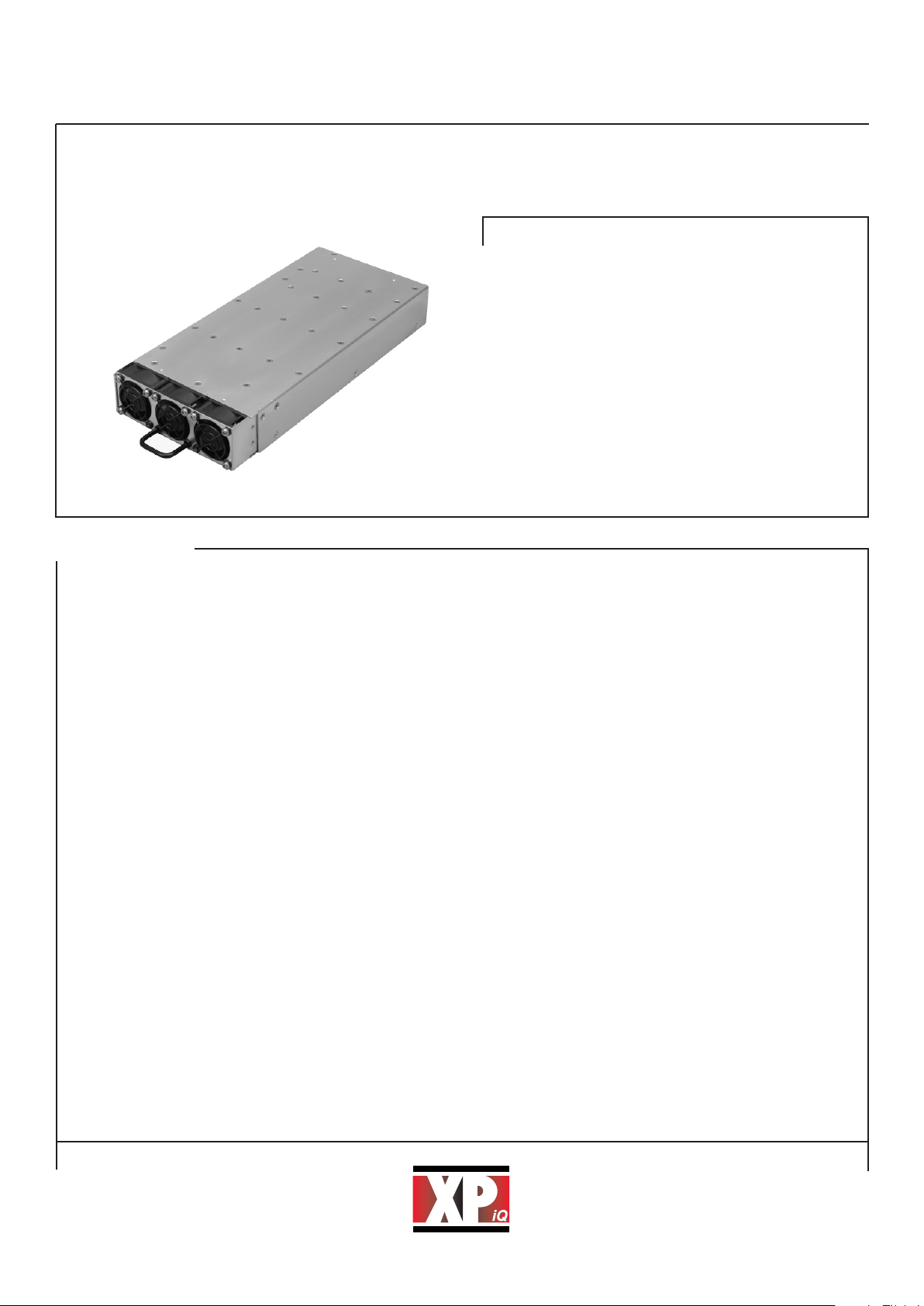
Size • 5.0” x 11.0” x 1.6”.
Weight • 3.3 lbs (1.5 kgs.)
Environmental
Operating • 0°C to 70°C, Full power to 50°C
Temperature derate from 50°C to 70°C
at 2.5%/°C
Cooling • 3 Internal ball bearing fans
Humidity • <95% RH, non-condensing
Storage Temperature • -40°C to +85°C
Safety and EMC
Safety Approvals • UL1950, CSA C22.2 No 950 per cUL,
EN60950 CE Mark LVD
EMI/EMC • EN61000-3-2, -3, EN55022 and FCC
20780 part 15J Class B conducted
with rack, Class A stand alone
Immunity & Surge • Meets EN61000-4-4, -5
600 Watts
ZC Series
Configurable Power Supply
Specification
•
Intelligent Design Quality Product
XPiQ inc.
Meets EN61000-3-2, -3
•
Up to 5 Outputs Plus 5V Standby
•
Low Voltage Outputs Down to 1.8V
•
Hot Swap or Chassis Mount
•
Oring Diodes On All Outputs
(Hot Swap Modules)
•
1U, 19” Rack Mount for 2 units
•
International Safety Approvals with CE (LVD)
PH: 508 429.9883
FAX: 800 226.2100
Email: sales@xpiq.com
Holliston, MA 01746 USA
www.XPiQ.com
ZC6.qxd 6/6/03 4:03 pm Page 1
Mechanical Details
CODE V1 V2 V3 CODE V4 CODE V5
01 1.8 V @ 70 A 2.5 V @ 50 A 12 V @ 10A PA +3.3 V @ 3 A PD +1.8 V @ 3 A
02 1.8 V @ 70 A 3.3 V @ 50 A 12 V @ 10A NA -3.3 V @ 3 A ND -1.8 V @ 3 A
03 1.8 V @ 70 A 5.0 V @ 50 A 12 V @ 10A PB +5.0 V @ 3 A PE +2.5 V @ 3 A
04 2.5 V @ 100 A - 12 V @ 10A NB -5.0 V @ 3 A NE -2.5 V @ 3 A
05 2.5 V @ 70 A 3.3 V @ 50 A 12 V @ 10A PC +12.0 V @ 3 A PF +3.3 V @ 3 A
06 2.5 V @ 70 A 5.0 V @ 50 A 12 V @ 10A NC -12.0 V @ 3 A NF -3.3 V @ 3 A
07 3.3 V @ 100 A - 12 V @ 10A - - PG +5.0 V @ 3 A
08 3.3 V @ 70 A 2.5 V @ 50 A 12 V @ 10A - - NG -5.0 V @ 3 A
09 3.3 V @ 70 A 5.0 V @ 50 A 12 V @ 10A - - PH +5.2 V @ 3 A
10 5.0 V @ 100 A - 12 V @ 10A - - NH -5.2 V @ 3 A
11 5.0 V @ 70 A 2.5 V @ 50 A 12 V @ 10A - - - 12 5.0 V @ 70 A 3.3 V @ 50 A 12 V @ 10A - - - -
13 1.8 V @ 70 A 2.5 V @ 50 A 5 V @ 10A XX N/C PD +1.8 V @ 3 A
14 1.8 V @ 70 A 3.3 V @ 50 A 5 V @ 10A - - ND -1.8 V @ 3 A
15 2.5 V @ 100 A 5 V @ 10A - - - 16 2.5 V @ 50 A 3.3 V @ 50 A 5 V @ 10A - - - 17 3.3 V @ 100 A 5 V @ 10A - - - 18 2.5 V @ 50 A 2.5 V @ 50 A 5 V @ 10A - - - -
ORDERING CODES ZC
1. For module codes 13 to 18, V4 may have an unregulated output but this output is not useable. XX is the only option code available for
V4 and only ±1.8V output is available for V5.
2. V4 is user adjustable from 2.8 VDC to 14.75 VDC codes define setpoint at factory.
3. V5 is user adjustable from 1.7 VDC to 8.12 VDC codes define setpoint at factory.
Notes
•
PART NUMBER ORDERING SCHEME
Series AC or DC Hotswap or V1-V3 Polarity V4 Output Polarity of V5 Output Option
Input Chassis Code of V4 Code V5 Code Code
ZC A6=AC H=Hotswap 01 to 18 P = Positive A to C P = Positive D to H L = Low Leakage
D6=DC C=Chassis N = Negative N = Negative I = I
2
C Module
M = Low Leakage
&12C
Example: ZCA6H06NCNG is AC input, Hotswap chassis with V1 = 2.5V/70A, V2 = 5V/50A, V3 = 12V/10A, V4 = -12V/3A, V5 = -5V/3A.
* Note:
Vertical blackplane mounting
may not allow for sufficient
airflow. Horizontal backplane,
or additional spacing with a
vertical backplane is
recommended.
PH: 508 429.9883
FAX: 800 226.2100
Email: sales@xpiq.com
Holliston, MA 01746 USA
www.XPiQ.com
ZC6.qxd 6/6/03 4:03 pm Page 2

Model Input Connector Description Input
ZC6A-1U2R-DFI Dual Front IEC320 with Switch
ZC6A-1U2R-DRI Dual Rear IEC320 with Switch
ZC6A-1U2R-SFI
(1)
Single Front IEC320 with Switch
ZC6A-1U2R-SRI
(1)
Single Rear IEC320 with Switch
AC
ZC6A-1U2R-DFT Dual Front Terminal Block
ZC6A-1U2R-DRT Dual Rear Terminal Block
ZC6A-1U2R-SFT Single Front Terminal Block
ZC6A-1U2R-SRT Single Rear Terminal Block
ZC6D-1U2R-DFT Dual Front Terminal Block
ZC6D-1U2R-DRT Dual Rear Terminal Block
DC
ZC6D-1U2R-SFT Single Front Terminal Block
ZC6D-1U2R-SRT Single Rear Terminal Block
STANDARD RACK MODELS
1. OK for 1+1 Redundant operation or total output power to 1000W.
2. Add -C for Clear Plastic Rear Safety Cover.
Notes
•
PIN STAGING
Pins Length
1-20 0.300”
21-26 0.250”
27 0.150”
28-44 0.250”
45-47 0.450
MATING CONNECTOR BOARD
Has mating Positronics connector
and terminal block connections for
AC input, DC outputs and control
and monitoring signals.
Order No. ZC6 INTBD
PIN CONNECTIONS
Pin Function Pin Function
1 +V1 Out 25 Spare
2 +V1 Out 26 +5V, 1A Standby
3 +V1 Out 27 Enable*
4 +V1 Out 28 Spare
5 +V1 Out 29 V1 External Trim
6 +V1 Out 30 +V1 Sense
7 V1 & V2 Return 31 -V1 Sense
8 V1 & V2 Return 32 V2 External Trim
9 V1 & V2 Return 33 +V2 Sense
10 V1 & V2 Return 34 -V2 Sense
11 V1 & V2 Return 35 V1 Current Share
12 V1 & V2 Return 36 +V3 Sense
13 V1 & V2 Return 37 -V3 Sense
14 +V2 Out 38 DC Power Good
15 +V2 Out 39 Global Inhibit
16 +V2 Out 40 Overtemp. Warning
17 +V2 Out 41 V2 Current Share
18 +V2 Out 42 AC Power Fail
19 V3 Return 43 Spare
20 +V3 Out 44 V3 Current Share
21 V4 Out 45 Chassis Ground
22 Signal Ground 46 AC Line
23 V5 Out 47 AC Neutral
24 V4 & V5 Return
Note: * For unit to operate, pin 27 must be at TTL LO or
shorted to pin 22. All returns and signal ground are
connected together.
Application Notes
1. Maximum power must not exceed the following: 500 watts for V1 and V2 combined,
171 watts for V3, V4 and V5 combined, or 600W for total unit.
2. For units with V1 over 70 amps, that output actually consists of the V1 and V2 outputs
in parallel. In this mode the V1 and V2 output pins must be connected to one another
and the V1 and V2 current share pins connected to each other. The V1 plus sense and
minus sense pins are connected to the V2 plus sense and minus sense pins,
respectively. All connections are external to unit.
3. The DC Power Good signal monitors the V1, V2 and V3 outputs only.
4. DESCRIPTION and INTERCONNECTION OF LOGIC SIGNALS
ENABLE, DC POWER GOOD, AC POWER FAIL, OVERTEMP WARNING and INHIBIT pin
connections come from the equivalent of an open collector circuit with an internal pull
up 10K resister to +5V.
ENABLE. Pin must be shorted to ground in order for outputs to function. The connection
may also be achieved by means of an external open collector or open FET drain circuit,
i.e., when the external transistor is turned on, the power supply is enabled. This is the
inverse of the inhibit function below.
DC POWER GOOD. Provides Logic High signal when V1, V2 and V3 reach a prescribed level.
AC POWER FAIL. Provides a Logic High signal pulse when the AC line voltage ceases.
Pulse occurs a minimum of 4 milliseconds before outputs go out of regulation. Pulse
duration is 4 milliseconds up to tens of milliseconds depending on load. Signal is logic
high rather than low (typical in non-redundant power supplies) so that there is no signal
ambiguity when redundant power supplies are operated from different AC phases.
OVERTEMP WARNING. Provides a Logic High signal when exit air temperature approaches
an unacceptable level.
GLOBAL INHIBIT. Shuts down the outputs but not the standby supply or the fans. As with
the Enable pin above, it is achieved by shorting the pin to ground or turning on an external
transistor. Acts as the inverse of the Enable pin.
5. Connecting all output signals together for units in an N+1 Rack. Normally signals are used
for identifying status of each module in paralleled unit configuration. If it is desired to
connect all the signals together to treat the complete rack as a single power supply, the
following (or equivalent) must be done. The AC Power Fail, DC Power Good and Overtemp
Warning signals of each module are each connected to the anode of a BAV99 diode, the
other side of which goes to the base of a 2N2222A. The collectors of all the AC Power Fail
transistors are connected to form a single AC Power Fail chassis signal. The same is done
for the DC Power Good and Overtemp Warning signals. The resultant system signals are
then provided in a Logic Low form.
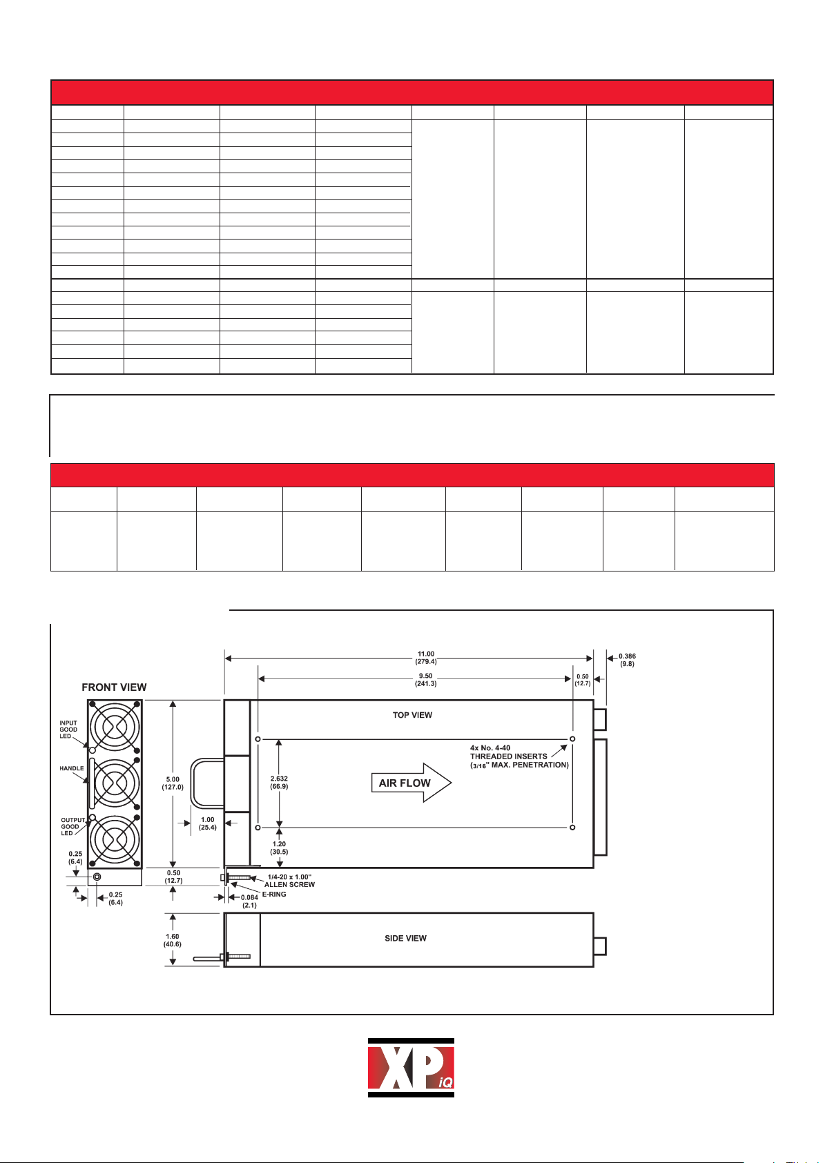
All Dimensions in Inches (mm)
Pin Connections
Output Connector: Positronics PCIH47M400A1
Mates with: Positronics PCIH47F80000
PH: 508 429.9883
FAX: 800 226.2100
Email: sales@xpiq.com
Holliston, MA 01746 USA
www.XPiQ.com
ZC6.qxd 6/6/03 4:03 pm Page 3

P1 PIN CONNECTIONS
Pins Function Pins Function
A1 V3 Common 5 V4
A2 +V3 6 -V3 Sense
A3 +V3 7 -V2 Sense
1 +V3 Sense 8 -V1 Sense
2 +V2 Sense 9 V5 Common
3 +V1 Sense 10 V5
4 V4 Common
P2 PIN CONNECTIONS
Pins Function Pins Function
1 Inhibit-B 14 Input Power Fail-B
2 Output Good/Data-B 15 Serial Clock-B
3 5V Standby-B 16 Interrupt-B
4 Module Present-B 17 Common
5 Spare 1 18 +V3 Sense
6 Spare 2 19 -V3 Sense
7 Spare 3 20 +V2 Sense
8 -V1 Sense 21 -V2 Sense
9 +V1 Sense 22 Module Present-A
10 Common 23 Interrupt-A
11 +5V Standby-A 24 Serial Clock-A
12 Output Good/Data-A 25 Input Power Fail A
13 Inhibit-A
Mechanical Details - 19 Inch Rack
NOTES:
1. All outputs from the two modules are
connected in parallel in the rack except the +5V 1A
standby outputs which must be externally paralleled
by connecting P2 pins 3 and 11 together.
2. The V1 and V2 Returns and V3, V4 and V5 Commons
are all connected together in the rack. It is recommended,
however, that the Returns and Commons be separately
connected to their respective loads.
3. For details on I
2
C data (P2 pins 2, 12, 15, 16, 23 & 24),
contact factory.
4. The Module Present outputs (P2 pins 4 & 22) are grounded
when the module is plugged in.
5. Front view below shows dual IEC320 connectors; back
view shows dual terminal block connectors.
6. Module A is on the left; module B is on the right.
7. Dual-feed input isolation diodes can be provided.
Please contact factory.
8. For dual input racks, each input goes separately to the module
on the same side of the rack.
All dimensions in inches (mm)
Front View
Back View
PH: 508 429.9883
FAX: 800 226.2100
Email: sales@xpiq.com
Holliston, MA 01746 USA
www.XPiQ.com
ZC6.qxd 6/6/03 4:03 pm Page 4
 Loading...