

INTERNATIONAL MICROCIRCUITS C9869 User Manual
Preliminary
C9869
Low EMI Clock Generator for Intel 815 Chipset Systems
Product Features
• Designed for Intel’s 815 chipset
• 2 copies of CPU Clock (CPU[0:1])
• 13 copies of SDRAM Clock (SDRAM[0:12])
• 7 copies of PCI Clocks
• 3 copies of 3V66 Clock
• 1 IOAPIC Clock, synchronous to PCI Clock
• 1 REF Clock
• 1 USB Clock (Non SSC), 1 DOT Clock (Non SSC)
• IMI Spread Spectrum for best EMI reduction
• Dial-a-Frequency™ Feature
• Dial-a-Skew™ Feature
• Dial-a-dB™ Feature
• Dial-a-Drive™ Feature
• 56 Pin SSOP
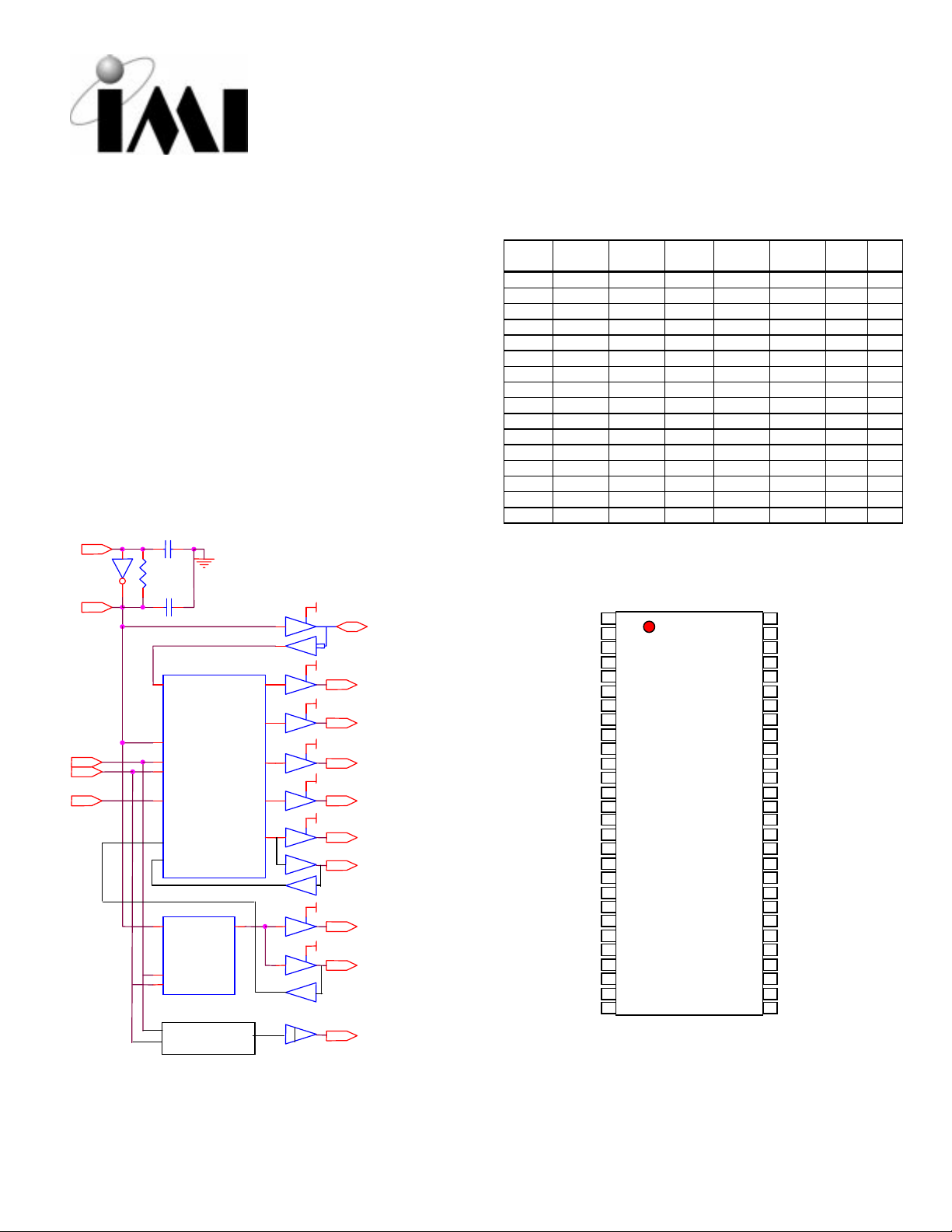
Block Diagram
XOUT
SCLK
SDATA
SEL0
XIN
300K
S1
Rin
i2c-clk
i2c-data
s0
s2
s3
Rin 48
i2c-clk
i2c-data
PLL2
36pF
36pF
PLL1
System
Recovery
apic
cpu
sdram
3V66
VDD
1
VDDI
1
2
13
3
pci
4
1
1
1
IOAPIC
VDDC
CPU(0:1)
VDDS
SDRAM(0:12)
VDD
3V66(0:2)
VDD
PCI(1:6)
PCI0/Sel 3
VDD
DOT
VDD
USB/Sel2
SRESET
REF / Se l 1
Frequency Table (MHz)
SEL
(3:0) CPU SDRAM 3V66
0000 66.67 100.00* 66.67 33.33 14.318M 48M 48M
0001 100.00 100.00* 66.67 33.33 14.318M 48M 48M
0010 133.33 133.33 66.67 33.33 14.318M 48M 48M
0011 133.33 100.00* 66.67 33.33 14.318M 48M 48M
0100 83.35 125.02 83.35 41.67 14.318M 48M 48M
0101 106.91 106.91 71.27 35.64 14.318M 48M 48M
0110 150.00 150.00 75.00 37.50 14.318M 48M 48M
0111 120.96 120.96 80.64 40.32 14.318M 48M 48M
1000 89.90 134.86 89.90 44.95 14.318M 48M 48M
1001 125.02 125.02 83.35 41.67 14.318M 48M 48M
1010 200.00 200.00 100.00 50.00 14.318M 48M 48M
1011 116.87 116.87 77.91 38.96 14.318M 48M 48M
1100 100.00 133.33 66.67 33.33 14.318M 48M 48M
1101 112.00 112.00 74.67 37.33 14.318M 48M 48M
1110 166.53 166.53 83.27 41.63 14.318M 48M 48M
1111 140.00 105.00 70.00 35.00 14.318M 48M 48M
Table1
*Will be set to 133 MHz, I2C Byte3, Bit0 is set to a Logic 1.
PCI
/IOAPIC REF DOT USB
Pin Configuration
IOAPIC 1 56 VSS
VDDI 2 55 VDDC
VSS 3 54 CPU0
REF / Sel1 4 53 CPU1
VDD 5 52 VSS
Xin 6 51 SDRAM0
Xout 7 50 SDRAM1
VSS 8 49 VDDS
VDD 9 48 VSS
3V66-0 10 47 SDRAM2
3V66-1 11 46 SDRAM3
3V66-2 12 45 SDRAM4
VSS 13 44 SDRAM5
PCI0 / Sel3 14 43 VDDS
PCI1 15 42 VSS
PCI2 16 41 SDRAM6
VDD 17 40 SDRAM7
VSS 18 39 SDRAM8
PCI3 19 38 SDRAM9
PCI4 20 37 VDDS
PCI5 21 36 VSS
PCI6 22 35 SDRAM10
Sel0 23 34 SDRAM11
VSS 24 33 SDRAM12
VDD 25 32 SRESET
SCLK 26 31 DOT
SDATA 27 30 USB / Sel2
VSS 28 29 VDD
Fig.1
INTERNATIONAL MICROCIRCUITS, INC. 525 LOS COCHES ST., Rev 1.0 10/17/2000
MILPITAS, CA 95035, USA. TEL: 408-263-6300, FAX 408-263-6571 Page 1 of 18
http://www.imicorp.com
C9869
Low EMI Clock Generator for Intel 815 Chipset Systems
Preliminary
Pin Description
PIN No. Pin Name PWR I/O TYPE Description
1
4
6
7
14
15, 16, 19, 20,
21, 22
10, 11, 12
30
31
23
27
26
32
33,34,35,38,
39,40,41,44,
45,46,47,50,51
53, 54
5,9,17,25,29
55, 2
3,8,13,18,24,
28,36,42,48,
52,56
37,43,49
PU = Internal Pull-Up. Typical 250KΩ (range 200KΩ to 500KΩ). PD = Internal Pull-Down. Typical 50KΩ (range 20KΩ to 70KΩ)
IOAPIC
SEL1 / REF
XIN
XOUT
SEL3 / PCI0
PCI(1:6)
3V66(0:2)
SEL2 / USB
DOT
SEL0
SDATA
SCLK
SRESET
SDRAM
(0:12)
CPU(0:1)
VDD
VDDC,VDDI
VSS
VDDS
VDDI O 2.5V IOAPIC clock output. See fig.3 p.4 for timing relationship.
VDD I/O PD This is a bi-directional pin (see app. note, p.6). At power up, it is an
input pin Sel1 for frequency selection (see table 1 p.1). When the
power reaches the rail, the state of Sel1 is latched, and this pin
becomes REF, a buffer output of the signal applied at Xin, typically
14.318MHz.
VDD I OSC1 On-chip reference oscillator input pin. Requires either an external
parallel resonant crystal (nominally 14.318 MHz) or externally
generated reference signal
VDD O On-chip reference oscillator pin. Drives an external parallel resonant
crystal. When an externally generated reference signal is used at Xin,
this pin remains unconnected.
VDD I/O PD This is a bi-directional pin (see app. note, p.6). At power up, it is an
input pin Sel3 for frequency selection (see table 1 p.1). When the
power reaches the rail, the state of Sel3 is latched, and this pin
becomes PCI clock output.
VDD O 3.3V PCI clock outputs. They are Synchronous to CPU clocks. See
fig.3, page4.
VDD O 3.3V Hub/AGP clock outputs. See fig.3 page 4.
VDD I/O PD This is a bi-directional pin (see app. note, p.6). At power up, it is an
input pin Sel2 for frequency selection (see table 1 p.1). When the
power reaches the rail, the state of Sel2 is latched, and this pin
becomes a fixed 48MHz clock output for USB.
VDD O 3.3V Fixed 48 MHz DOT clock output.
VDD I PU 3.3V LVTTL inputs for frequency selection, see table 1 page 1. Sel0
also controls TS# functionality if TS# is 0 during power up (See pg.7).
VDD I Serial data input pin. Conforms to the Philips I2C specification of a
Slave Receive/Transmit device. This pin is an input when receiving
data. It is an open drain output when acknowledging or transmitting
data. See I2C function description, pp. 8,9,10.
VDD I Serial clock input pin. Conforms to the Philips I2C specification.
VDD O
Reset Open Drain Output. This active low output generates a
3ms pulse for system reset when programmed by the device.
VDDS O 3.3V SDRAM DIMM clocks. See table1, p.1 for frequency selection.
See fig.3, page 4 for timing relationship and I
VDDC O 2.5V Host clock outputs. See table1,p.1 for frequency selection.
- 3.3V Common Power Supply
- 2.5V Power Supply for CPU(0:1) and IOAPIC clock respectively.
- - Common Ground pins.
- - 3.3V power support for SDRAM(0:12) clock output drivers.
2
C Byte3, Bit0.
INTERNATIONAL MICROCIRCUITS, INC. 525 LOS COCHES ST., Rev 1.0 10/17/2000
MILPITAS, CA 95035, USA. TEL: 408-263-6300, FAX 408-263-6571 Page 2 of 18
http://www.imicorp.com
C9869
Low EMI Clock Generator for Intel 815 Chipset Systems
Preliminary
Test Mode Function
Test Mode Functionality
TS# SEL0 CPU (0:1) SDRAM (0:12) 3V66 (0:2) PCI (_F, 1:5) DOT/USB REF IOAPIC
0 1 TCLK/2 TCLK/2 TCLK/3 TCLK/6 TCLK/2 TCLK TCLK/6
0 0 Tristate Tristate Tristate Tristate Tristate Tristate Tristate
Table 2
Note
:
TCLK is a test clock over driven on the XIN input during test mode.
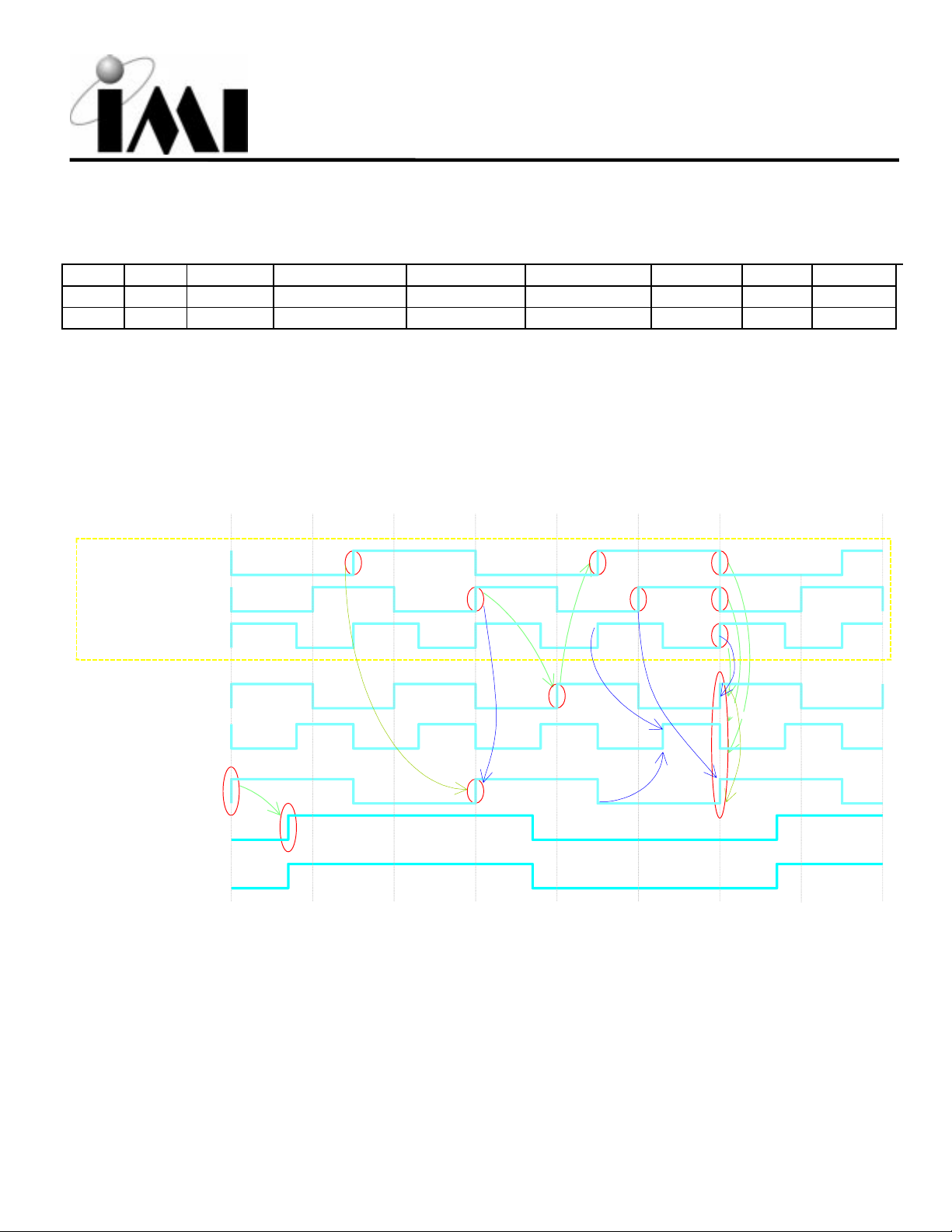
Clock Phase Relationships
0nS 10nS 20nS 30nS 40nS
CPU CLOCK
CPU CLOCK
CPU CLOCK
SDRAM CLOCK
SDRAM CLOCK
3V66 CLOCK
PCI CLOCK
IOAPIC CLOCK
66MHz
100MHz
133MHz
100MHz
133MHz
66MHz
33MHz
33MHz
1.5~3.5nS
7.5nS
Fig.2
5nS
0nS
2.5nS
3.75nS
Sync
0nS
5nS
0nS
3.75nS
INTERNATIONAL MICROCIRCUITS, INC. 525 LOS COCHES ST., Rev 1.0 10/17/2000
MILPITAS, CA 95035, USA. TEL: 408-263-6300, FAX 408-263-6571 Page 3 of 18
http://www.imicorp.com
Low EMI Clock Generator for Intel 815 Chipset Systems
Preliminary
Group Timing Relationships and Tolerances
CPU = 66.6 MHz, SDRAM = 100 MHz
Offset (nS) Tolerance (pS) Conditions
CPU to SDRAM 2.5 500 SDRAM leads
CPU to 3V66 7.5 500 180 degrees phase shift
SDRAM to 3V66 0 500 When rising edges line-up
3V66 to PCI 1.5-3.5 500 3V66 leads
PCI to IOAPIC 0 1000
CPU = 100 MHz, SDRAM = 100 MHz
Offset (nS) Tolerance (pS) Conditions
CPU to SDRAM 5 500 180 degrees phase shift
CPU to 3V66 5 500
SDRAM to 3V66 0 500 When rising edges line-up
3V66 to PCI 1.5-3.5 500 3V66 leads
PCI to IOAPIC 0 1000
CPU = 133.3 MHz, SDRAM = 100 MHz
Offset (nS) Tolerance (pS) Conditions
CPU to SDRAM 0 500 When rising edges line-up
CPU to 3V66 0 500
SDRAM to 3V66 0 500 When rising edges line-up
3V66 to PCI 1.5-3.5 500 3V66 leads
PCI to IOAPIC 0 1000
CPU = 133.3 MHz, SDRAM = 133.3 MHz
Offset (nS) Tolerance (pS) Conditions
CPU to SDRAM 3.75 500 180 degrees phase shift
CPU to 3V66 0 500
SDRAM to 3V66 3.75 500
3V66 to PCI 1.5-3.5 500 3V66 leads
PCI to IOAPIC 0 1000
C9869
INTERNATIONAL MICROCIRCUITS, INC. 525 LOS COCHES ST., Rev 1.0 10/17/2000
MILPITAS, CA 95035, USA. TEL: 408-263-6300, FAX 408-263-6571 Page 4 of 18
http://www.imicorp.com
C9869
Select Data is latched into register, then pin becomes a clock output signal.
Low EMI Clock Generator for Intel 815 Chipset Systems
Preliminary
Power on Bi-Directional Pins
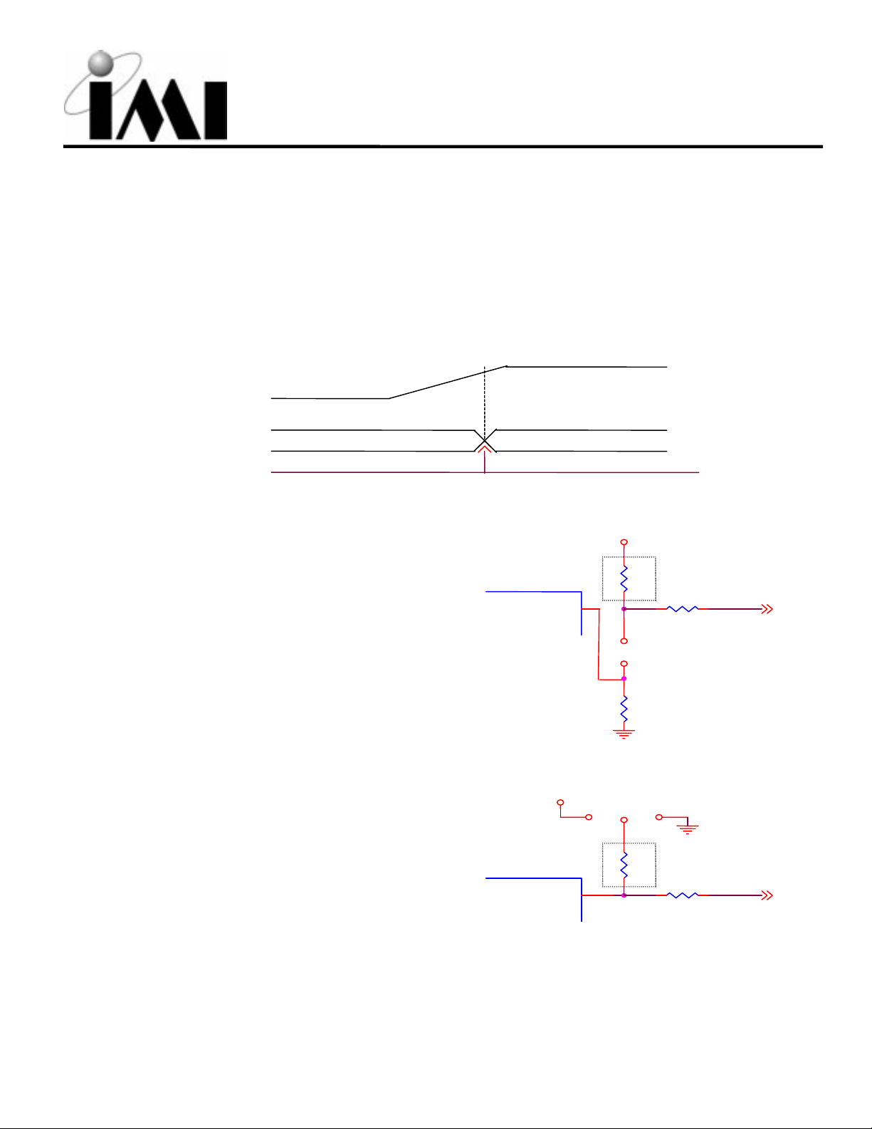
Power Up Condition:
Pins 4, 14, 30 are Power up bi-directional pins and are used for selecting the host frequency in page 1, table 1. During
power-up of the device, these pins are in input mode (see Fig 4, below), therefore; they are considered input select pins,
Sel(1:3) internal to the IC. After a settling time, the selection data is latch into the internal control register and these pins
become a clock output.
Power Supply
Ramp
REF / SEL1(Pin 4)
PCI0 / SEL3 (Pin14)
Hi-Z Inputs Toggle Outputs
USB / SEL2 (30)
Strapping Resistor Options:
The power up bi-directional pins have a large value pulldown (50K
Ω+/−20KΩ)
, therefore, a selection “0” is the
default. If the system uses a slow power supply (over
10mS settling time), then
it is recommended
to use an
external Pull-down (Rdn) in order to insure a low
selection. In this case, the designer m ay choose one of
two configurations, see Fig.4A and B.
Fig. 4A represents an additional pull down resistor 5K
Ω
connected from the pin to the power line, which allows a
faster down to a high level.
If a selection “1” is desired, then a jumper is placed on
JP1 to a 1 KΩ resistor as shown in Fig.4A. Please note
the selection resistors (Rup and Rdn) are placed before
the Damping resistor (Rd) close to the pin.
Fig. 4B represent a single resistor 5KΩ connected to a
3-way jumper, JP2. W hen a “1” selection is desired, a
jumper is placed between leads1 and 3. When a “0”
selection is desired, a jumper is placed between leads 1
and 2.
Fig.3
-
IMI C9869
Bidirectional
IMI C9869
Bidirectional
Vdd
Vdd
Rup
1K
JP1
JUMPER
Rdn
5K
JP2
3 W ay Jum per
1
Rsel
5K
VDD Rail
23
Rd
Rd
Load
Fig. 4A
Load
Fig. 4B
INTERNATIONAL MICROCIRCUITS, INC. 525 LOS COCHES ST., Rev 1.0 10/17/2000
MILPITAS, CA 95035, USA. TEL: 408-263-6300, FAX 408-263-6571 Page 5 of 18
http://www.imicorp.com
C9869
Low EMI Clock Generator for Intel 815 Chipset Systems
Preliminary
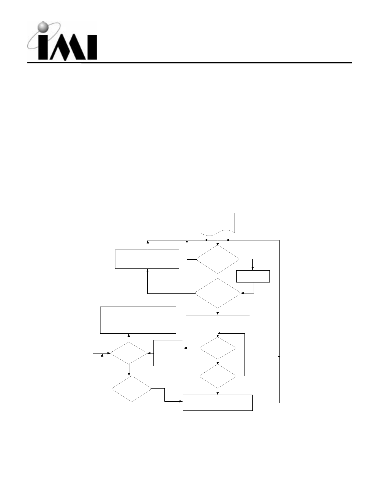
System Self Recovery Clock Management:
This feature is designed to allow the system designer to change frequency while the system is running and reboot the
operation of the system in case of a hang up due to the frequency change.
When the system s ends an I
2
C command reques ting a frequenc y change through Byte 0, it must have previously sent a
command to byte 5, bits (3:0) to select which time out stamp the watch dog mus t perform, otherwise the System Self
Recovery feature will not be applicable. Consequently, this device will change frequency and then the watch dog timer
starts timing. Meanwhile, the system BIOS is running its operation with the new frequency selected via I
receives a new I
watch dog times out, then this device will keep operating in its normal condition with the new selected frequency. If the
watch dog times out the first time before the new I
2
C command to clear the bits or iginally program med in Byte 5, bits (3:0) (reprogram to 0000), bef ore the
2
C reprograms Byte 5, bits (3:0) to (0000), then this devic e will send a
2
C. If this device
3mS low system reset pulse and changes WD alarm (Byte5, Bit4) status to “1” then restarts the watch dog timer again. If
the watch dog times out a second tim e, then this device will send another 3mS low pulse on SRESET, relatch original
hardware strapping frequency selection, set W D alarm bit (Byte5, bit4) to ‘1’, then start WD timer again. The above
described sequence will keep repeating until the BIOS c lears the I2C bytes5 bits(3:0). Once the BIOS s ets Byte 5 bits
(3:0) = 0000, then the watch dog timer is turned off and the WD alarm bit (Byte 5, bit4) is reset to’0’.
System running with
originally selected
frequency via
hardware strapping.
Frequency will change but System Self
Recovery not applicable (no time stamp
selected and byte 5, bit(3:0) is still =
"0000"
No
No
Receive Frequency
Change Request via I2C
Byte 0?
Is I2C Byte 5, time out
stamp enabled - (byte 5, bit
(3:0) 0000)?
≠
Yes
Change to a new
frequency
1) Send another 3mS low pulse on SRESET
2) Relatch original hardware strapping selection
for return to original frequency settings.
3) Set WD Alarm bit (byte 5, Bit4) to "1"
4) Start WD timer
Yes
1) Send SRESET
pulse
Watch Dog time out?
No
I2C byte 5 time out
stamp disabled, Byte 5,
No
bit(3:0) = (0000)?
2) Set WD bit
(byte 5, bit4) to '1'
3) Start WD timer
Yes
Turn off watch dog timer.
Keep new frequency setting. Set WD alarm
bit (byte 5, bit4) to ''0'
Start internal watch dog timer.
Yes
Watch Dog time out?
Yes
No
I2C byte 5 time out
stamp disabled?
Yes
No
Fig. 5
INTERNATIONAL MICROCIRCUITS, INC. 525 LOS COCHES ST., Rev 1.0 10/17/2000
MILPITAS, CA 95035, USA. TEL: 408-263-6300, FAX 408-263-6571 Page 6 of 18
http://www.imicorp.com
 Loading...