*Other brands and names are the property of their respective owners.
Information in this document is provided in connection with Intel products. Intel assumes no liability whatsoever, including infringement of any patent or
copyright, for sale and use of Intel products except as provided in Intel’s Terms and Conditions of Sale for such products. Intel retains the right to make
changes to these specifications at any time, without notice. Microcomputer Products may have minor variations to this specification known as errata.
May 1994COPYRIGHT©INTEL CORPORATION, 1995 Order Number: 271305-001
VE28F008
8 MBIT (1 MBIT x 8) FLASH MEMORY
Y
High-Density Symmetrically Blocked
Architecture
Ð Sixteen 64 Kbyte Blocks
Y
Avionics Temperature Range
Ð
b
40§Ctoa125§C
Y
Extended Cycling Capability
Ð 10K Block Erase Cycles
Ð 160K Block Erase
Cycles per Chip
Y
Automated Byte Write and Block Erase
Ð Command User Interface
Ð Status Register
Y
System Performance Enhancements
Ð RY/BY
Status Output
Ð Erase Suspend Capability
Y
Very High-Performance Read
Ð 95 ns Maximum Access Time
Y
SRAM-Compatible Write Interface
Y
Hardware Data Protection Feature
Ð Erase/Write Lockout during Power
Transitions
Y
Industry Standard Packaging
Ð 40-Lead TSOP
Y
ETOXTMIII Nonvolatile Flash
Technology
Ð 12V Byte Write/Block Erase
Y
Independent Software Vendor Support
Ð Microsoft* Flash File System (FFS)
Intel’s VE28F008 8-Mbit Flash FileTMMemory revolutionizes the design of high performance and durable
mass storage memory systems for the Industrial, Avionics and Military markets. With its innovative features
like low power, blocked architecture, high read/write performance, and expanded temperature range, any
design, or mission, is free from the dependence on battery backed up memory or highly sensitive and slow
rotating media drives.
Using the VE28F008 in a PCMCIA 2.1 Flash Memory card, ATA drive or any size or shape module will allow
data, application, or operating systems to be updated or collected anywhere, and at anytime. This data on
demand feature ensures protection from obsolesce through field or in system software updates.
The VE28F008’s highly integrated Command User Interface and Write State Machine, decreases the size and
complexity of system software while providing high read, write and erase performance. The sixteen separately
erasable 64 Kbyte blocks along with a multiple write data protection system, provides assurance that highly
important data will be available when needed.
The VE28F008 is offered in a 40-lead TSOP (Thin Small Outline Package) which is capable of performing in
temperatures from
b
40§Ctoa125§C. It employs advanced CMOS circuitry for systems requiring low power
consumption and noise immunity. The VE28F008’s 95 ns access time provides superior performance when
compared to magnetic mass storage
Manufactured on Intel’s 0.8 micron ETOXTMIII process, the VE28F008 provides the highest levels of quality,
reliability and cost effectiveness.
*Microsoft is a trademark of Microsoft Corporation.

VE28F008
PRODUCT OVERVIEW
The VE28F008 is a high-performance 8 Mbit
(8,388,608 bit) memory organized as 1 Mbyte
(1,048,576 bytes) of 8 bits each. Sixteen 64 Kbyte
(65,536 byte) blocks are included on the VE28F008.
A memory map is shown in Figure 4 of this specification. A block erase operation erases one of the sixteen blocks of memory in typically 1.6 seconds, independent of the remaining blocks. Each block can
be independently erased and written 10,000 cycles.
Erase Suspend mode allows system software to
suspend block erase to read data or execute code
from any other block of the VE28F008.
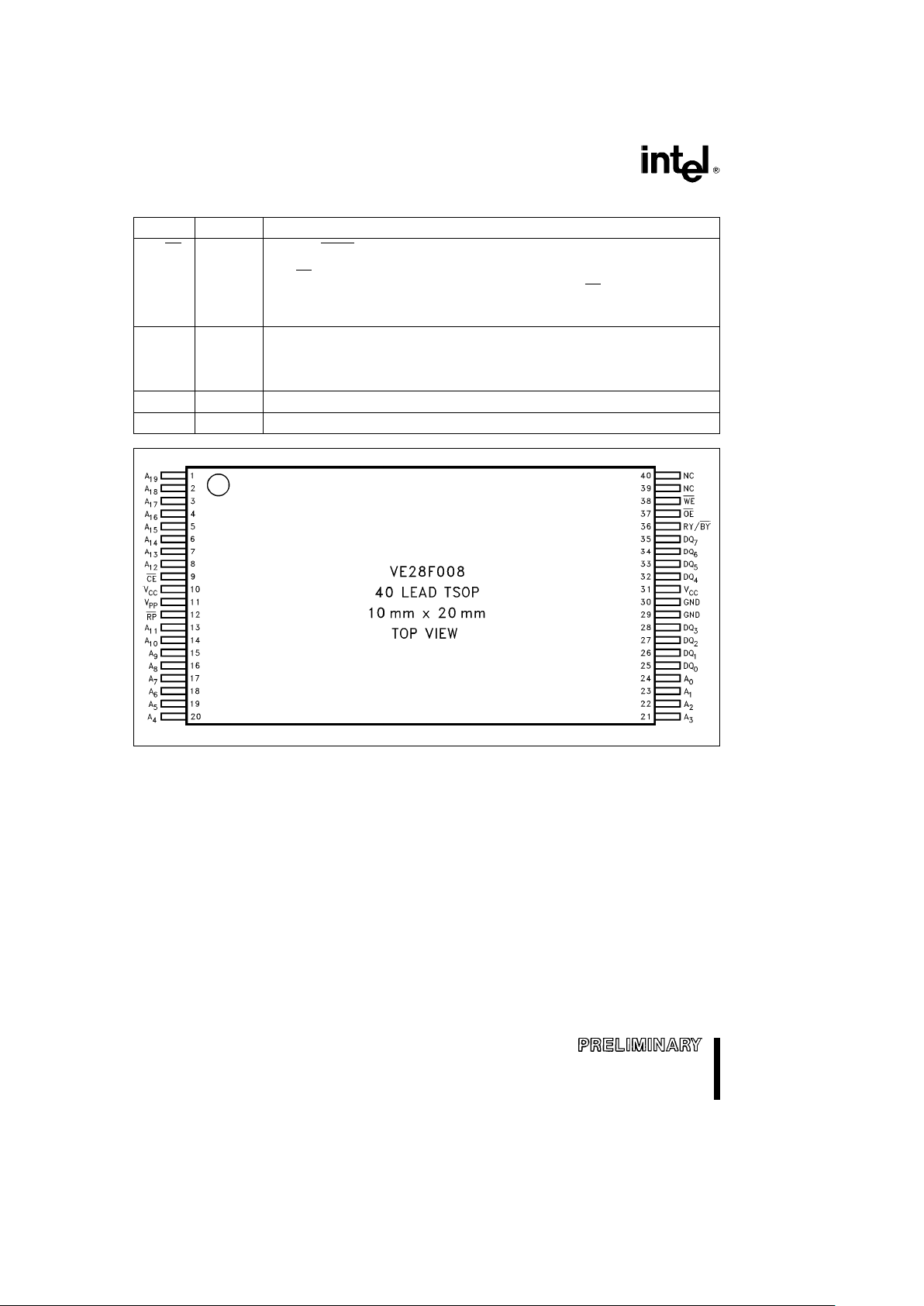
The VE28F008 is available in a 40-lead TSOP package. Pinout is shown in Figure 2 of this specification.
The Command User Interface serves as the interface between the microprocessor or microcontroller
and the internal operation of the VE28F008.
Byte Write and Block Erase Automation allow
byte write and block erase operations to be executed using a two-write command sequence to the
Command User Interface. The internal Write State
Machine (WSM) automatically executes the algorithms and timings necessary for byte write and
block erase operations, including verifications,
thereby unburdening the microprocessor or microcontroller. Writing of memory data is performed in
byte increments typically within 9 ms, an 80% improvement over current flash memory products. I
PP
byte write and block erase currents are 30 mA
maximum. V
PP
byte write and block erase volt-
age is 11.4V to 12.6V.
The Status Register indicates the status of the
WSM and when the WSM successfully completes
the desired byte write or block erase operation.
The RY/BY
output gives an additional indicator of
WSM activity, providing capability for both hardware
signal of status (versus software polling) and status
masking (interrupt masking for background erase,
for example). Status polling using RY/BY minimizes
both CPU overhead and system power consumption. When low, RY/BY
indicates that the WSM is
performing a block erase or byte write operation.
RY/BY
high indicates that the WSM is ready for new
commands, block erase is suspended or the device
is in deep powerdown mode.
Maximum access time is 95 ns (t
ACC
) over the avi-
onics temperature range (
b
40§Ctoa125§C) and
over V
CC
supply voltage range 4.75V to 5.25V. I
CC
active current (CMOS Read) is 35 mA maximum
at 8 MHz.
When the CE
and RP pins are at VCC, the ICCCMOS
Standby mode is enabled.
A Deep Powerdown mode is enabled when the RP
pin is at GND, minimizing power consumption and
providing write protection. Reset time of 400 ns is
required from RP
switching high until outputs are valid to read attempts. Equivalently, the device has a
wake time of 1 m s from RP
high until writes to the
Command User Interface are recognized by the
VE28F008. With RP
at GND, the WSM is reset and
the Status Register is cleared.
2

VE28F008
271305– 1
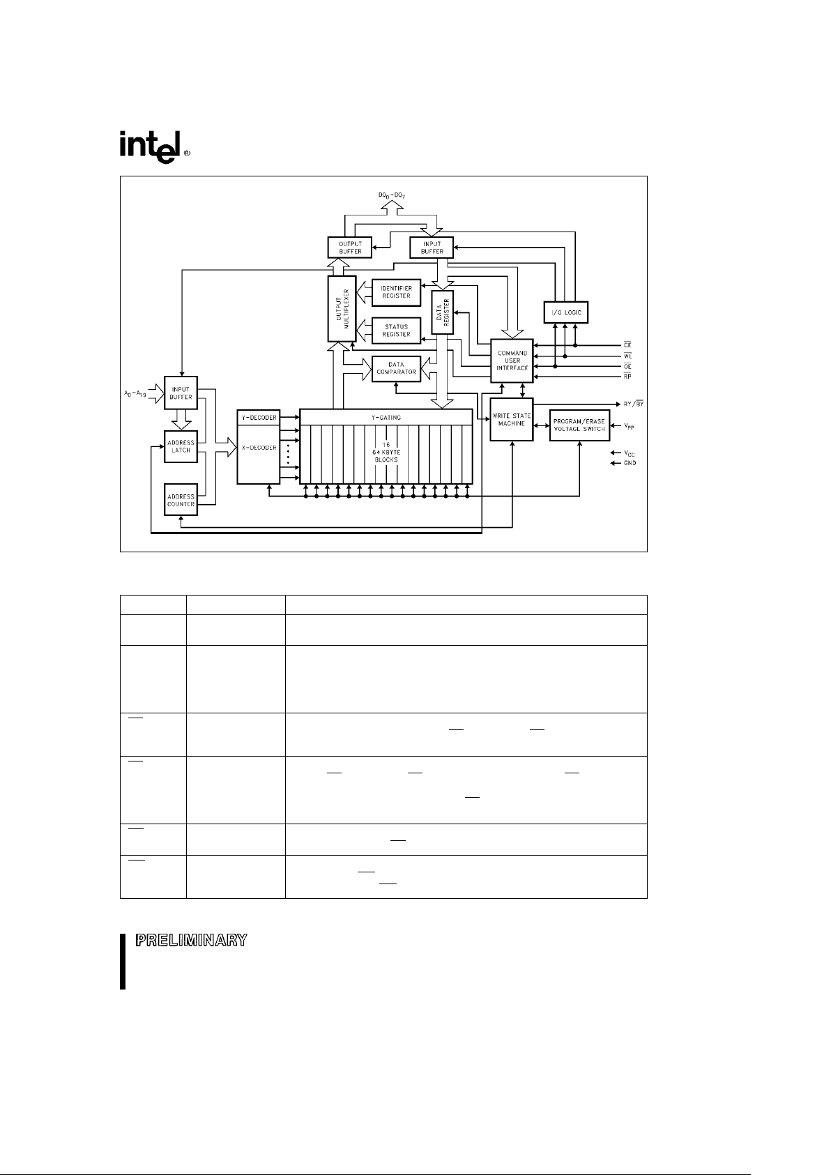
Figure 1. Block Diagram
Table 1. Pin Description
Symbol Type Name and Function
A0–A
19
INPUT ADDRESS INPUTS for memory addresses. Addresses are internally
latched during a write cycle.
DQ0–DQ7INPUT/OUTPUT DATA INPUT/OUTPUTS: Inputs data and commands during Command
User Interface write cycles; outputs data during memory array, Status
Register and Identifier read cycles. The data pins are active high and
float to tri-state off when the chip is deselected or the outputs are
disabled. Data is internally latched during a write cycle.
CE INPUT CHIP ENABLE: Activates the device’s control logic, input buffers,
decoders, and sense amplifiers. CE
is active low; CE high deselects the
memory device and reduces power consumption to standby levels.
RP INPUT RESET/DEEP POWERDOWN: Puts the device in the deep powerdown
mode. RP
is active low. RP high gates normal operation. RP also locks
out block erase or byte write operations when active low, providing data
protection during power transitions. RP
active resets internal
automation. Exit from Deep Powerdown sets device to read-array mode.
OE INPUT OUTPUT ENABLE: Gates the device’s outputs through the data buffers
during a read cycle. OE
is active low.
WE INPUT WRITE ENABLE: Controls writes to the Command User Interface and
array blocks. WE
is active low. Addresses and data are latched on the
rising edge of the WE pulse.
3

VE28F008
Table 1. Pin Description (Continued)
Symbol Type Name and Function
RY/BY OUTPUT READY/BUSY: Indicates the status of the internal Write State Machine. When
low, it indicates that the WSM is performing a block erase or byte write operation.
RY/BY
high indicates that the WSM is ready for new commands, block erase is
suspended or the device is in deep powerdown mode. RY/BY
is always active and
does NOT float to tri-state off when the chip is deselected or data outputs are
disabled.
V
PP
BLOCK ERASE/BYTE WRITE POWER SUPPLY for erasing blocks of the array
or writing bytes of each block.
NOTE:
With V
PP
k
V
PPLMAX
, memory contents cannot be altered.
V
CC
DEVICE POWER SUPPLY (5Vg5%)
GND GROUND
271305– 2
Figure 2. TSOP Pinout
4

VE28F008
271305– 3
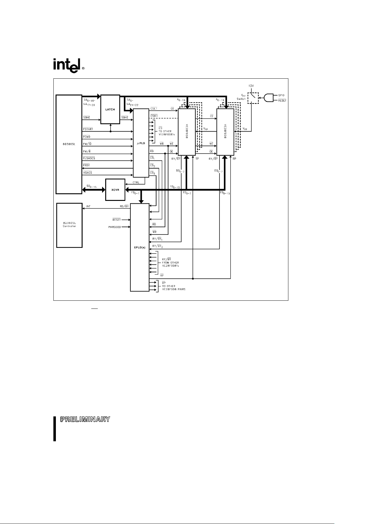
Figure 3. VE28F008 Array Interface to Intel386TMSL Microprocessor Superset through PI Bus
(Including RY/BY
Masking and Selective Powerdown), for DRAM Backup during System SUSPEND,
Resident O/S and Applications and Motherboard Solid-State Disk.
PRINCIPLES OF OPERATION
The VE28F008 includes on-chip write automation to
manage write and erase functions. The Write State
Machine allows for: 100% TTL-level control inputs,
fixed power supplies during block erasure and byte
write, and minimal processor overhead with RAMlike interface timings.
After initial device powerup, or after return from
deep powerdown mode (see Bus Operations), the
VE28F008 functions as a read-only memory. Manipulation of external memory-control pins allow array
read, standby and output disable operations. Both
Status Register and intelligent identifier can
also be accessed through the Command User Interface when V
PP
e
V
PPL
.
This same subset of operations is also available
when high voltage is applied to the V
PP
pin. In addi-
tion, high voltage on V
PP
enables successful block
erasure and byte writing of the device. All functions
associated with altering memory contentsÐbyte
write, block erase, status and intelligent identifierÐ
are accessed via the Command User Interface and
verified thru the Status Register.
Commands are written using standard microprocessor write timings. Command User Interface contents
serve as input to the WSM, which controls the block
5

VE28F008
erase and byte write circuitry. Write cycles also internally latch addresses and data needed for byte write
or block erase operations. With the appropriate command written to the register, standard microprocessor read timings output array data, access the intelligent identifier codes, or output byte write and block
erase status for verification.
Interface software to initiate and poll progress of internal byte write and block erase can be stored in
any of the VE28F008 blocks. This code is copied to,
and executed from, system RAM during actual flash
memory update. After successful completion of byte
write and/or block erase, code/data reads from the
VE28F008 are again possible via the Read Array
command. Erase suspend/resume capability allows
system software to suspend block erase to read
data and execute code from any other block.
FFFFF
64 Kbyte Block
EFFFF
F0000
64 Kbyte Block
DFFFF
E0000
64 Kbyte Block
CFFFF
D0000
64 Kbyte Block
BFFFF
C0000
64 Kbyte Block
AFFFF
B0000
64 Kbyte Block
9FFFF
A0000
64 Kbyte Block
8FFFF
90000
64 Kbyte Block
7FFFF
80000
64 Kbyte Block
6FFFF
70000
64 Kbyte Block
5FFFF
60000
64 Kbyte Block
4FFFF
50000
64 Kbyte Block
3FFFF
40000
64 Kbyte Block
2FFFF
30000
64 Kbyte Block
1FFFF
20000
64 Kbyte Block
0FFFF
10000
64 Kbyte Block
00000
Figure 4. Memory Map
Command User Interface and Write
Automation
An on-chip state machine controls block erase and
byte write, freeing the system processor for other
tasks. After receiving the Erase Setup and Erase
Confirm commands, the state machine controls
block pre-conditioning and erase, returning progress
via the Status Register and RY/BY
output. Byte
write is similarly controlled, after destination address
and expected data are supplied. The program and
erase algorithms of past Intel Flash memories are
now regulated by the state machine, including pulse
repetition where required and internal verification
and margining of data.
Data Protection
Depending on the application, the system designer
may choose to make the V
PP
power supply switchable (available only when memory byte writes/block
erases are required) or hardwired to V
PPH
. When
V
PP
e
V
PPL
, memory contents cannot be altered.
The VE28F008 Command User Interface architecture provides protection from unwanted byte write or
block erase operations even when high voltage is
applied to V
PP
. Additionally, all functions are dis-
abled whenever V
CC
is below the write lockout volt-
age V
LKO
, or when RP is at VIL. The VE28F008 accommodates either design practice and encourages
optimization of the processor-memory interface.
The two-step byte write/block erase Command User
Interface write sequence provides additional software write protection.
BUS OPERATION
Flash memory reads, erases and writes in-system
via the local CPU. All bus cycles to or from the flash
memory conform to standard microprocessor bus
cycles.
Read
The VE28F008 has three read modes. The memory
can be read from any of its blocks, and information
can be read from the intelligent identifier or Status
Register. V
PP
can be at either V
PPL
or V
PPH
.
The first task is to write the appropriate read mode
command to the Command User Interface (array, intelligent identifier, or Status Register). The
VE28F008 automatically resets to Read Array mode
upon initial device powerup or after exit from deep
powerdown. The VE28F008 has four control pins,
two of which must be logically active to obtain
6

VE28F008
Table 2. Bus Operations
Mode Notes RP CE OE WE A0V
PP
DQ
0–7
RY/BY
Read 1, 2, 3 V
IH
V
IL
V
ILVIH
XXD
OUT
X
Output Disable 3 V
IH
V
ILVIHVIH
X X High Z X
Standby 3 V
IH
V
IH
X X X X High Z X
PowerDown V
IL
X X X X X High Z V
OH
Intelligent Identifier (Mfr) V
IH
V
ILVIL
V
IH
V
IL
X 89H V
OH
Intelligent Identifier (Device) V
IH
V
ILVIL
V
IH
V
IH
X A2H V
OH
Write 3, 4, 5 V
IH
V
ILVIHVIL
XX DINX
NOTES:
1. Refer to DC Characteristics. When V
PP
e
V
PPL
, memory contents can be read but not written or erased.
2. X can be V
IL
or VIHfor control pins and addresses, and V
PPL
or V
PPH
for VPP. See DC Characteristics for V
PPL
and V
PPH
voltages.
3. RY/BY
is VOLwhen the Write State Machine is executing internal block erase or byte write algorithms. It is VOHwhen the
WSM is not busy, in Erase Suspend mode or deep powerdown mode.
4. Command writes involving block erase or byte write are only successfully executed when V
PP
e
V
PPH
.
5. Refer to Table 3 for valid D
IN
during a write operation.
data at the outputs. Chip Enable (CE) is the device
selection control, and when active enables the selected memory device. Output Enable (OE
)isthe
data input/output (DQ
0
–DQ7) direction control, and
when active drives data from the selected memory
onto the I/O bus. RP
and WE must also be at VIH.
Figure 8 illustrates read bus cycle waveforms.
Output Disable
With OE at a logic-high level (VIH), the device outputs are disabled. Output pins (DQ
0
–DQ7) are
placed in a high-impedance state.
Standby
CE at a logic-high level (VIH) places the VE28F008
in standby mode. Standby operation disables much
of the VE28F008’s circuitry and substantially reduces device power consumption. The outputs (DQ
0
–
DQ
7
) are placed in a high-impedence state indepen-
dent of the status of OE
. If the VE28F008 is deselected during block erase or byte write, the device
will continue functioning and consuming normal active power until the operation completes.
Deep Power-Down
The VE28F008 offers a deep powerdown feature,
entered when RP
is at VIL. During read modes, RP at
a logic-low level (V
IL
) deselects the memory, places
output drivers in a high-impedence state and turns
off all internal circuits. The VE28F008 requires time
t
PHQV
(see AC Characteristics-Read-Only Operations) after return from powerdown until initial memory access outputs are valid. After this wakeup interval, normal operation is restored. The Command
User Interface is reset to Read Array mode, and the
upper 5 bits of the Status Register are cleared to
value 10000, upon return to normal operation.
During block erase or byte write modes, RP
at a log-
ic-low level (V
IL
) will abort either operation. Memory
contents of the block being altered are no longer
valid as the data will be partially written or erased.
Time t
PHWL
after RP goes to logic-high (VIH) is re-
quired before another command can be written.
Intelligent Identifier Operation
The intelligent identifier operation outputs the manufacturer code, 89H; and the device code, A2H for
the VE28F008. The system CPU can then automatically match the device with its proper block erase
and byte write algorithms.
The manufacturer and device codes are read via the
Command User Interface. Following a write of 90H
to the Command User Interface, a read from address location 00000H outputs the manufacturer
code (89H). A read from address location 00001H
outputs the device code (A2H). It is not necessary to
have high voltage applied to V
PP
to read the intelli-
gent identifier from the Command User Interface.
7

VE28F008
Table 3. Command Definitions
Command Cycles
Req’d
Bus
Notes
First Bus Cycle Second Bus Cycle
Operation Address Data Operation Address Data
Read Array/Reset 1 1 Write X FFH
Intelligent Identifier 3 2, 3, 4 Write X 90H Read IA IID
Read Status Register 2 3 Write X 70H Read X SRD
Clear Status Register 1 Write X 50H
Erase Setup/Erase Confirm 2 2 Write BA 20H Write BA D0H
Erase Suspend/Erase Resume 2 Write X B0H Write X D0H
Byte Write Setup/Write 2 2, 3, 5 Write WA 40H Write WA WD
Alternate Byte Write Setup/Write 2 2, 3, 5 Write WA 10H Write WA WD
NOTES:
1. Bus operations are defined in Table 2.
2. IA
e
Identifier Address: 00H for manufacturer code, 01H for device code.
BA
e
Address within the block being erased.
WA
e
Address of memory location to be written.
3. SRD
e
Data read from Status Register. See Table 4 for a description of the Status Register bits.
WD
e
Data to be written at location WA. Data is latched on the rising edge of WE.
IID
e
Data read from intelligent identifiers.
4. Following the intelligent identifier command, two read operations access manufacture and device codes.
5. Either 40H or 10H are recognized by the WSM as the Byte Write Setup command.
6. Commands other than those shown above are reserved by Intel for future device implementations and should not be
used.
Write
Writes to the Command User Interface enable reading of device data and intelligent identifier. They also
control inspection and clearing of the Status Register. Additionally, when V
PP
e
V
PPH
, the Command
User Interface controls block erasure and byte write.
The contents of the interface register serve as input
to the internal write state machine.
The Command User Interface itself does not occupy
an addressable memory location. The interface register is a latch used to store the command and address and data information needed to execute the
command. Erase Setup and Erase Confirm commands require both appropriate command data and
an address within the block to be erased. The Byte
Write Setup command requires both appropriate
command data and the address of the location to be
written, while the Byte Write command consists of
the data to be written and the address of the location to be written.
The Command User Interface is written by bringing
WE
to a logic-low level (VIL) while CE is low. Addresses and data are latched on the rising edge of
WE
. Standard microprocessor write timings are
used.
Refer to AC Write Characteristics and the AC Waveforms for Write Operations, Figure 9, for specific timing parameters.
COMMAND DEFINITIONS
When V
PPL
is applied to the VPPpin, read operations from the Status Register, intelligent identifier,
or array blocks are enabled. Placing V
PPH
on V
PP
enables successful byte write and block erase operations as well.
Device operations are selected by writing specific
commands into the Command User Interface. Table
3 defines the VE28F008 commands.
Read Array Command
Upon initial device powerup and after exit from deep
powerdown mode, the VE28F008 defaults to Read
Array mode. This operation is also initiated by writing
FFH into the Command User Interface. Microprocessor read cycles retrieve array data. The device remains enabled for reads until the Command User
Interface contents are altered. Once the internal
Write State Machine has started a block erase or
byte write operation, the device will not recognize
8
 Loading...