Intel Corporation N83C196KD20, N87C196KD20, N87C196KD, N83C196KD, S83C196KD20 Datasheet
...
*Other brands and names are the property of their respective owners.
Information in this document is provided in connection with Intel products. Intel assumes no liability whatsoever, including infringement of any patent or
copyright, for sale and use of Intel products except as provided in Intel’s Terms and Conditions of Sale for such products. Intel retains the right to make
changes to these specifications at any time, without notice. Microcomputer Products may have minor variations to this specification known as errata.
November 1994COPYRIGHT©INTEL CORPORATION, 1995 Order Number: 272145-003
8XC196KD/8XC196KD20
COMMERCIAL CHMOS MICROCONTROLLER
87C196KDÐ32 Kbytes of On-Chip OTPROM
83C196KDÐ32 Kbytes of ROM
Y
16 MHz and 20 MHz Available
Y
1000 Byte Register RAM
Y
Register-to-Register Architecture
Y
28 Interrupt Sources/16 Vectors
Y
Peripheral Transaction Server
Y
1.4 ms 16 x 16 Multiply (20 MHz)
Y
2.4 ms 32/16 Divide (20 MHz)
Y
Powerdown and Idle Modes
Y
Five 8-Bit I/O Ports
Y
16-Bit Watchdog Timer
Y
Dynamically Configurable 8-Bit or
16-Bit Buswidth
Y
Full Duplex Serial Port
Y
High Speed I/O Subsystem
Y
16-Bit Timer
Y
16-Bit Up/Down Counter with Capture
Y
3 Pulse-Width-Modulated Outputs
Y
Four 16-Bit Software Timers
Y
8- or 10-Bit A/D Converter with
Sample/Hold
Y
HOLD/HLDA Bus Protocol
Y
OTP One-Time Programmable Version
The 8XC196KD 16-bit microcontroller is a high performance member of the MCSÉ96 microcontroller family.
The 8XC196KD is an enhanced 80C196KC device with 1000 bytes RAM, 16 MHz operation and an optional
32 Kbytes of ROM/EPROM. Intel’s CHMOS III process provides a high performance processor along with low
power consumption.
The 8XC196KD has a maximum guaranteed frequency of 16 MHz. The 8XC196KD20 has a maximum guaranteed frequency of 20 MHz. Unless otherwise noted, all references to the 8XC196KD also refer to the
8XC196KD20.
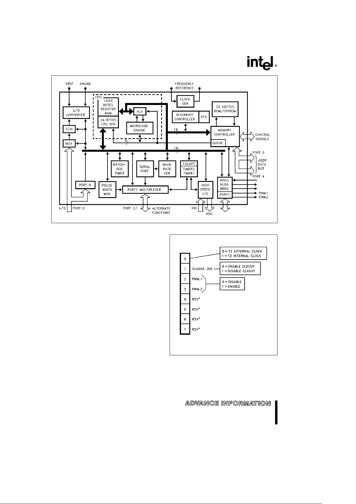
Four high-speed capture inputs are provided to record times when events occur. Six high-speed outputs are
available for pulse or waveform generation. The high-speed output can also generate four software timers or
start an A/D conversion. Events can be based on the timer or up/down counter.
8XC196KD/8XC196KD20
272145– 1
Figure 1. 8XC196KD Block Diagram
87C196KD ENHANCED FEATURE SET
OVER THE 87C196KC
1. The 87C196KD has twice the RAM and twice the
OTPROM space of the 87C196KC.
2. The vertical windowing scheme has been extended to allow all 1000 bytes of register RAM to be
windowed into the lower register file.
IOC3 (0CH HWIN1 READ/WRITE)
272145– 2
NOTE:
*RSVÐReserved bits must be
e
0
Figure 2. 87C196KD New SFR Bit
(CLKOUT Disable)
2
8XC196KD/8XC196KD20
8XC196KD VERTICAL WINDOWING
MAP
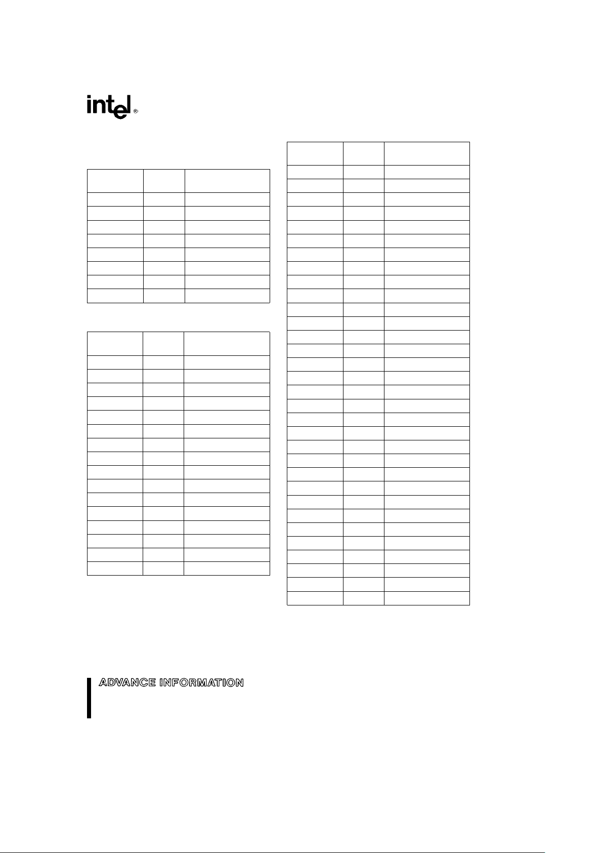
Table 1. 128-Byte Windows
Address to Device
WSR Contents
Remap Series
0380H KD X001 0111Be17H
0300H KD X001 0110Be16H
0280H KD X001 0101Be15H
0200H KD X001 0100Be14H
0180H KC, KD X001 0011Be13H
0100H KC, KD X001 0010Be12H
0080H KC, KD X001 0001Be11H
0000H KC, KD X001 0000Be10H
Window in Lower Register File: 80H–FFH
Table 2. 64-Byte Windows
Address to Device
WSR Contents
Remap Series
03C0H KD X010 1111Be2FH
0380H KD X010 1110Be2EH
0340H KD X010 1101Be2DH
0300H KD X010 1100Be2CH
02C0H KD X010 1011Be2BH
0280H KD X010 1010Be2AH
0240H KD X010 1001Be29H
0200H KD X010 1000Be28H
01C0H KC, KD X010 0111Be27H
0180H KC, KD X010 0110Be26H
0140H KC, KD X010 0101Be25H
0100H KC, KD X010 0100Be24H
00C0H KC, KD X010 0011Be23H
0080H KC, KD X010 0010Be22H
0040H KC, KD X010 0001Be21H
0000H KC, KD X010 0000Be20H
Window in Lower Register File: C0H–FFH
Table 3. 32-Byte Windows
Address to Device
WSR Contents
Remap Series
03E0H KD X101 1111Be5FH
03C0H KD X101 1110Be5EH
03A0H KD X101 1101Be5DH
0380H KD X101 1100Be5CH
0360H KD X101 1011Be5BH
0340H KD X101 1010Be5AH
0320H KD X101 1001Be59H
0300H KD X101 1000Be58H
02E0H KD X101 0111Be57H
02C0H KD X101 0110Be56H
02A0H KD X101 0101Be55H
0280H KD X101 0100Be54H
0260H KD X101 0011Be53H
0240H KD X101 0010Be52H
0220H KD X101 0001Be51H
0200H KD X101 0000Be50H
01E0H KC, KD X100 1111Be4FH
01C0H KC, KD X100 1110Be4EH
01A0H KC, KD X100 1101Be4DH
0180H KC, KD X100 1100Be4CH
0160H KC, KD X100 1011Be4BH
0140H KC, KD X100 1010Be4AH
0120H KC, KD X100 1001Be49H
0100H KC, KD X100 1000Be48H
00E0H KC, KD X100 0111Be47H
00C0H KC, KD X100 0110Be46H
00A0H KC, KD X100 0101Be45H
0080H KC, KD X100 0100Be44H
0060H KC, KD X100 0011Be43H
0040H KC, KD X100 0010Be42H
0020H KC, KD X100 0001Be41H
0000H KC, KD X100 0000Be40H
Window in Lower Register File: E0H–FFH
3
8XC196KD/8XC196KD20
PROCESS INFORMATION
This device is manufactured on PX29.5 or PX29.9, a
CHMOS III process. Additional process and reliability information is available in Intel’s
Components
Quality and Reliability Handbook,
Order Number
210997.
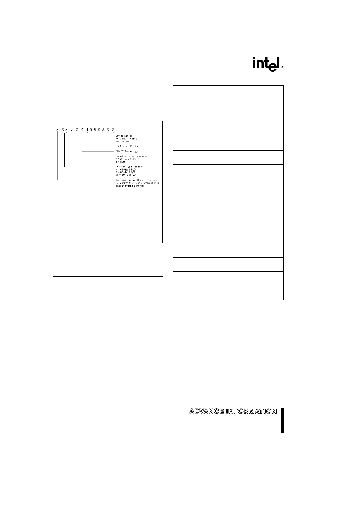
272145– 19
EXAMPLE: N87C196KD20 is 68-Lead PLCC
OTPROM, 20 MHz.
For complete package dimensional data, refer to the
Intel Packaging Handbook (Order Number 240800).
NOTE:
1. EPROMs are available as One Time Programmable
(OTPROM) only.
Figure 3. The 8XC196KD Family Nomenclature
Table 4. Thermal Characteristics
Package
i
ja
i
jc
Type
PLCC 35§C/W 13§C/W
QFP 56§C/W 12§C/W
SQFP 68§C/W 15.5§C/W
All thermal impedance data is approximate for static air
conditions at 1W of power dissipation. Values will change
depending on operation conditions and application. See
the Intel
Packaging Handbook
(order number 240800) for a
description of Intel’s thermal impedance test methodology.
Table 5. 8XC196KD Memory Map
Description Address
External Memory or I/O 0FFFFH
0A000H
Internal ROM/OTPROM or External 9FFFH
Memory (Determined by EA
)
2080H
Reserved. Must contain FFH. 207FH
(Note 5)
205EH
PTS Vectors 205DH
2040H
Upper Interrupt Vectors 203FH
2030H
ROM/OTPROM Security Key 202FH
2020H
Reserved. Must contain FFH. 201FH
(Note 5)
201AH
Reserved. Must Contain 20H 2019H
(Note 5)
CCB 2018H
Reserved. Must contain FFH. 2017H
(Note 5)
2014H
Lower Interrupt Vectors 2013H
2000H
Port 3 and Port 4 1FFFH
1FFEH
External Memory 1FFDH
0400H
1000 Bytes Register RAM (Note 1) 03FFH
0018H
CPU SFR’s (Notes 1, 3) 0017H
0000H
NOTES:
1. Code executed in locations 0000H to 03FFH will be
forced external.
2. Reserved memory locations must contain 0FFH unless
noted.
3. Reserved SFR bit locations must contain 0.
4. Refer to 8XC196KC for SFR descriptions.
5. WARNING: Reserved memory locations must not be
written or read. The contents and/or function of these locations may change with future revisions of the device.
Therefore, a program that relies on one or more of these
locations may not function properly.
4
8XC196KD/8XC196KD20
272145– 3
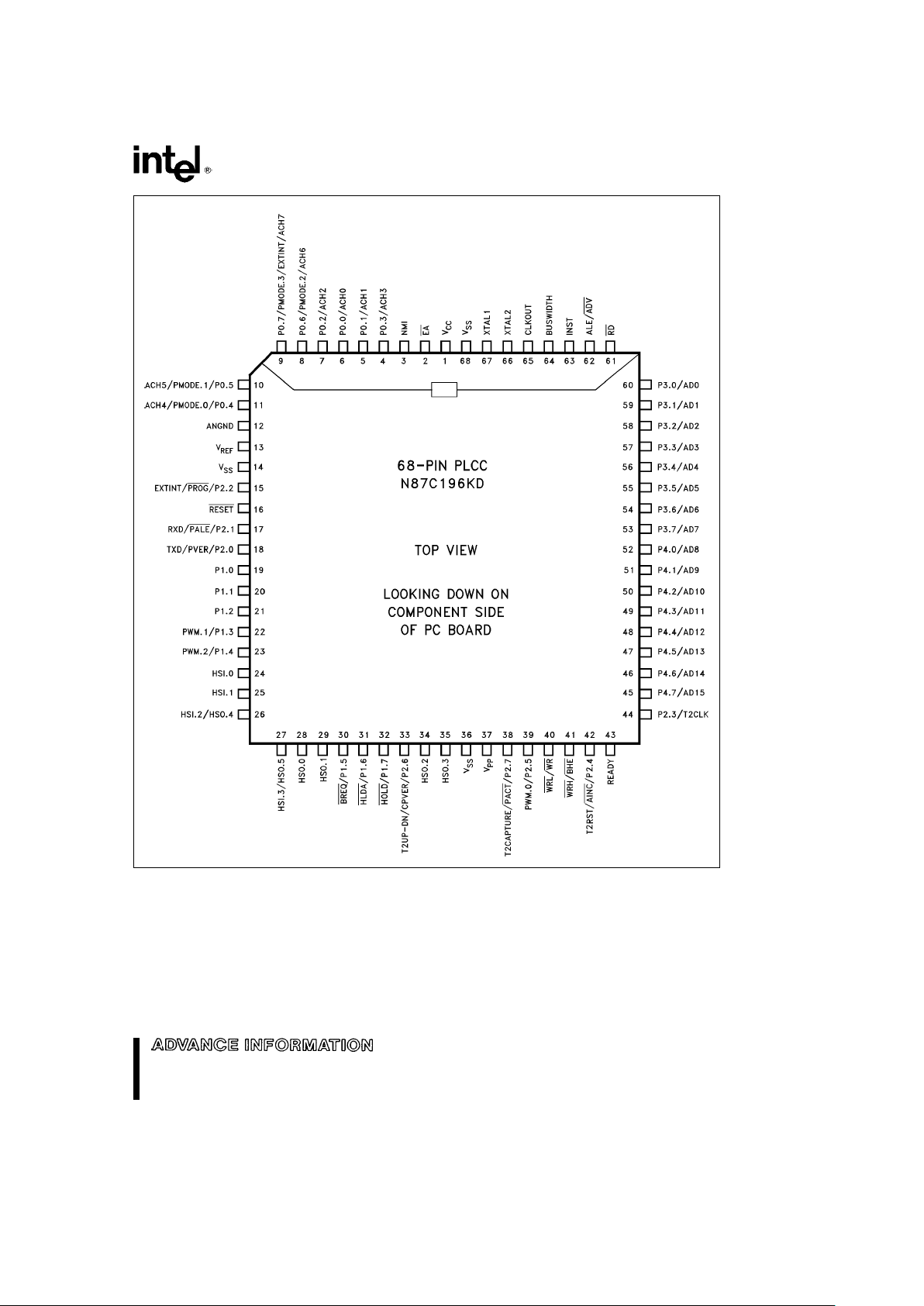
Figure 4. 68-Pin PLCC Package
5
8XC196KD/8XC196KD20
272145– 4
NOTE:
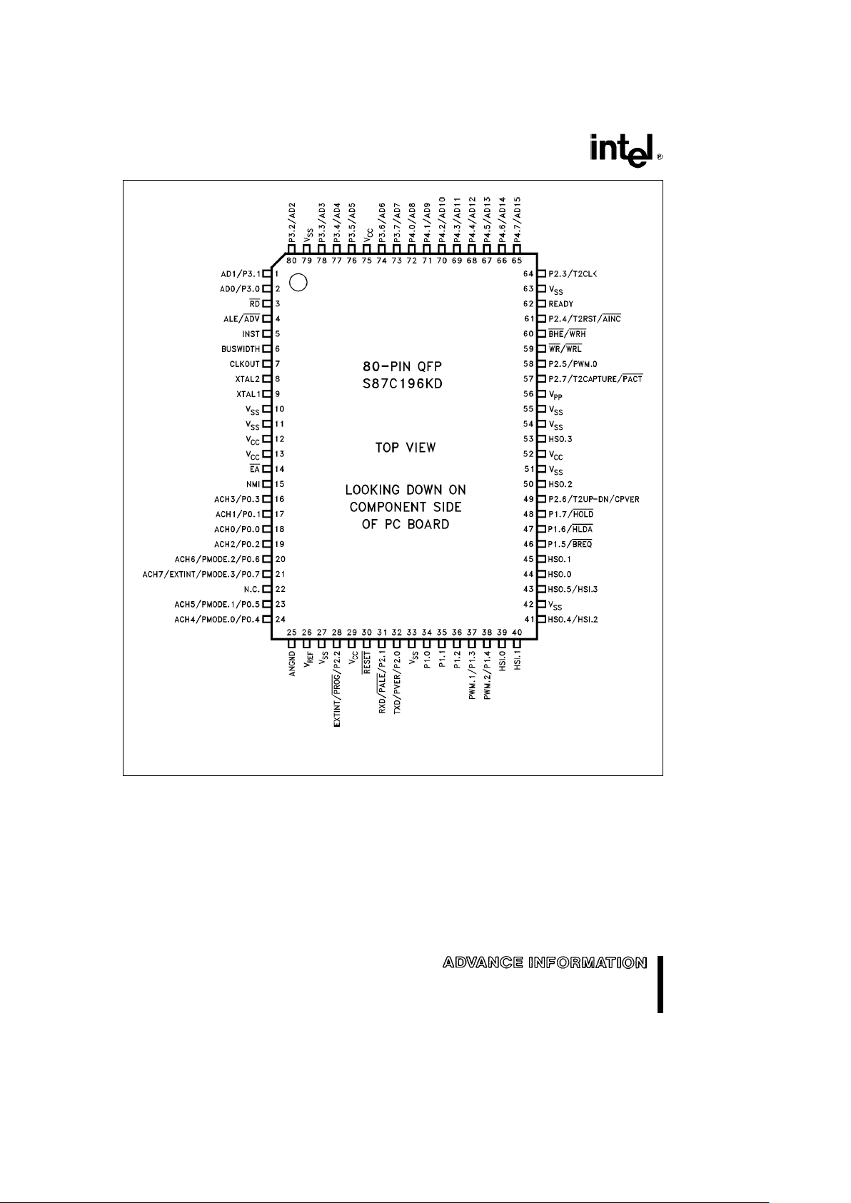
N.C. means No Connect (do not connect these pins).
Figure 5. 80-Pin QFP Package
6
8XC196KD/8XC196KD20
272145– 20
NOTE:
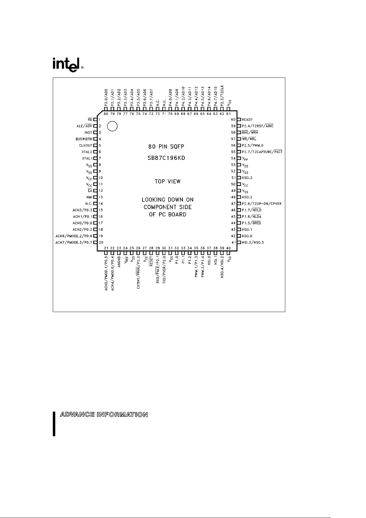
N.C. means No Connect (do not connect these pins).
Figure 6. 80-Pin SQFP Package
7
8XC196KD/8XC196KD20
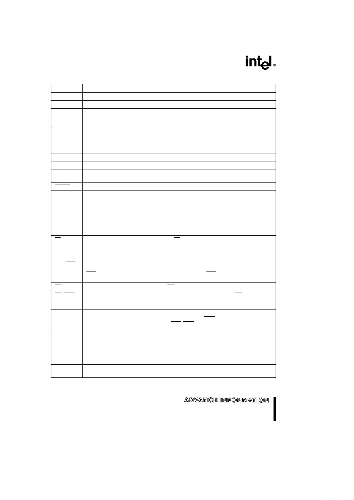
PIN DESCRIPTIONS
Symbol Name and Function
V
CC
Main supply voltage (5V).
V
SS
Digital circuit ground (0V). There are multiple VSSpins, all of which must be connected.
V
REF
Reference voltage for the A/D converter (5V). V
REF
is also the supply voltage to the analog
portion of the A/D converter and the logic used to read Port 0. Must be connected for A/D
and Port 0 to function.
ANGND Reference ground for the A/D converter. Must be held at nominally the same potential as
V
SS
.
V
PP
Timing pin for the return from powerdown circuit. This pin also supplies the programming
voltage on the EPROM device.
XTAL1 Input of the oscillator inverter and of the internal clock generator.
XTAL2 Output of the oscillator inverter.
CLKOUT Output of the internal clock generator. The frequency of CLKOUT is (/2 the oscillator
frequency.
RESET Reset input and open drain output.
BUSWIDTH Input for buswidth selection. If CCR bit 1 is a one, this pin selects the bus width for the bus
cycle in progress. If BUSWIDTH is a 1, a 16-bit bus cycle occurs. If BUSWIDTH isa0an
8-bit cycle occurs. If CCR bit 1 is a 0, the bus is always an 8-bit bus.
NMI A positive transition causes a vector through 203EH.
INST Output high during an external memory read indicates the read is an instruction fetch. INST
is valid throughout the bus cycle. INST is activated only during external memory accesses
and output low for a data fetch.
EA Input for memory select (External Access). EA equal high causes memory accesses to
locations 2000H through 9FFFH to be directed to on-chip ROM/EPROM. EA
equal low
causes accesses to those locations to be directed to off-chip memory. Also used to enter
programming mode.
ALE/ADV Address Latch Enable or Address Valid output, as selected by CCR. Both pin options
provide a signal to demultiplex the address from the address/data bus. When the pin is
ADV
, it goes inactive high at the end of the bus cycle. ALE/ADV is activated only during
external memory accesses.
RD Read signal output to external memory. RD is activated only during external memory reads.
WR/WRL Write and Write Low output to external memory, as selected by the CCR. WR will go low for
every external write, while WRL
will go low only for external writes where an even byte is
being written. WR
/WRL is activated only during external memory writes.
BHE/WRH Bus High Enable or Write High output to external memory, as selected by the CCR. BHE will
go low for external writes to the high byte of the data bus. WRH
will go low for external
writes where an odd byte is being written. BHE
/WRH is activated only during external
memory writes.
READY Ready input to lengthen external memory cycles, for interfacing to slow or dynamic
memory, or for bus sharing. When the external memory is not being used, READY has no
effect.
HSI Inputs to High Speed Input Unit. Four HSI pins are available: HSI.0, HSI.1, HSI.2 and HSI.3.
Two of them (HSI.2 and HSI.3) are shared with the HSO Unit.
HSO Outputs from High Speed Output Unit. Six HSO pins are available: HSO.0, HSO.1, HSO.2,
HSI.3, HSO.4 and HSO.5. Two of them (HSO.4 and HSO.5) are shared with the HSI Unit.
8
 Loading...