Intel Corporation N80C196MD, N83C196MD, N87C196MD, S80C196MD, S83C196MD Datasheet
...
*Other brands and names are the property of their respective owners.
Information in this document is provided in connection with Intel products. Intel assumes no liability whatsoever, including infringement of any patent or
copyright, for sale and use of Intel products except as provided in Intel’s Terms and Conditions of Sale for such products. Intel retains the right to make
changes to these specifications at any time, without notice. Microcomputer Products may have minor variations to this specification known as errata.
April 1994COPYRIGHT©INTEL CORPORATION, 1995 Order Number: 272323-002
8XC196MD
INDUSTRIAL MOTOR CONTROL
MICROCONTROLLER
87C196MD 16 Kbytes of On-Chip OTPROM*
87C196MD, ROM 16 Kbytes of On-Chip Factory-Programmed OTPROM
80C196MD ROMless
Y
High-Performance CHMOS 16-Bit CPU
Y
16 Kbytes of On-Chip OTPROM/
Factory-Programmed OTPROM
Y
488 bytes of On-Chip Register RAM
Y
Register to Register Architecture
Y
Up to 64 I/O Lines
Y
Peripheral Transaction Server (PTS)
with 17 Prioritized Sources
Y
Event Processor Array (EPA)
Ð 6 High Speed Capture/Compare
Modules
Ð 6 High Speed Compare Modules
Y
Extended Temperature Standard
Y
Programmable Frequency Generator
Y
Two 16-Bit Timers with Quadrature
Counting Input
Y
3-Phase Complementary Waveform
Generator
Y
14 Channel 8/10-Bit A/D with Sample/
Hold with Zero Offset Adjustment H/W
Y
18 Prioritized Interrupt Sources
Y
Flexible 8-/16-Bit External Bus
Y
1.75 ms 16 x 16 Multiply
Y
3 ms 32/16 Divide
Y
Idle and Power Down Modes
The 8XC196MD is a 16-bit microcontroller designed primarily to control 3 phase AC induction and DC brushless motors. The 8XC196MD is based on Intel’s MCS
É
96 16-bit microcontroller architecture and is manufac-
tured with Intel’s CHMOS process.
The 8XC196MD has a three phase waveform generator specifically designed for use in ‘‘Inverter’’ motor
control applications. This peripheral allows for pulse width modulation, three phase sine wave generation with
minimal CPU intervention. It generates 3 complementary non-overlapping PWM pulses with resolutions of
0.125 ms (edge trigger) or 0.250 m s (centered).
The 8XC196MD has 16 Kbytes on-chip OTPROM/ROM and 488 bytes of on-chip RAM. It is available in two
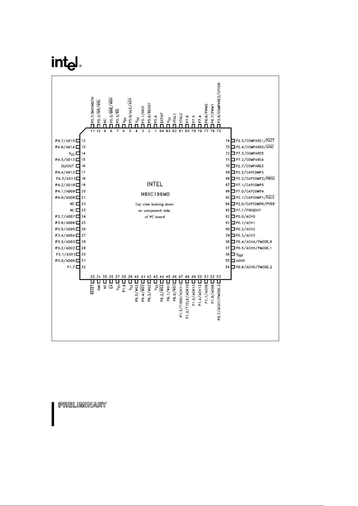
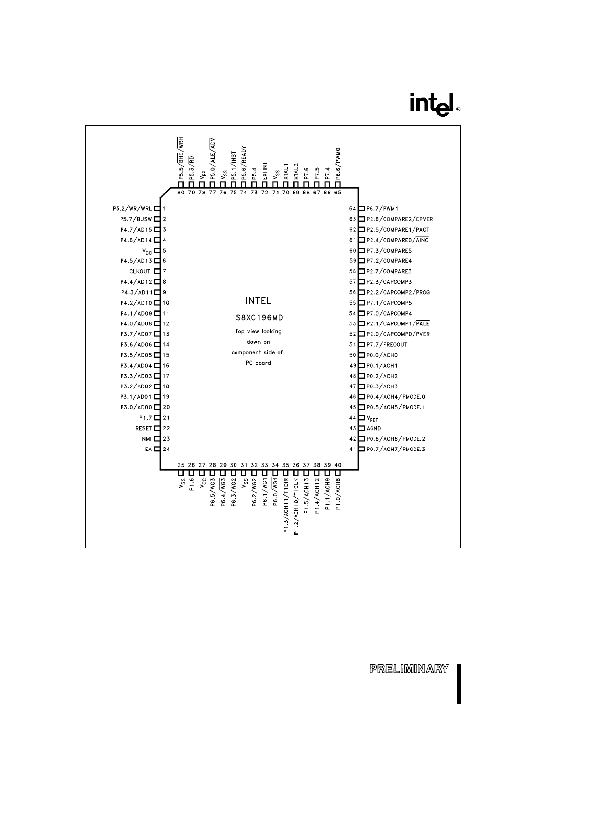
packages; PLCC (84-L) and EIAJ/QFP (80-L).
Operational characteristics are guaranteed over the temperature range of
b
40§Ctoa85§C.
The 87C196MD contains 16 Kbytes on-chip OTPROM. The 83C196MD contains 16 Kbytes on-chip ROM. All
references to the 80C196MD also refers to the 83C196MD and 87C196MD unless noted.
*OTPROM (One Time Programmable Read Only Memory) is the same as EPROM but it comes in an unwindowed package
and cannot be erased. It is user programmable.
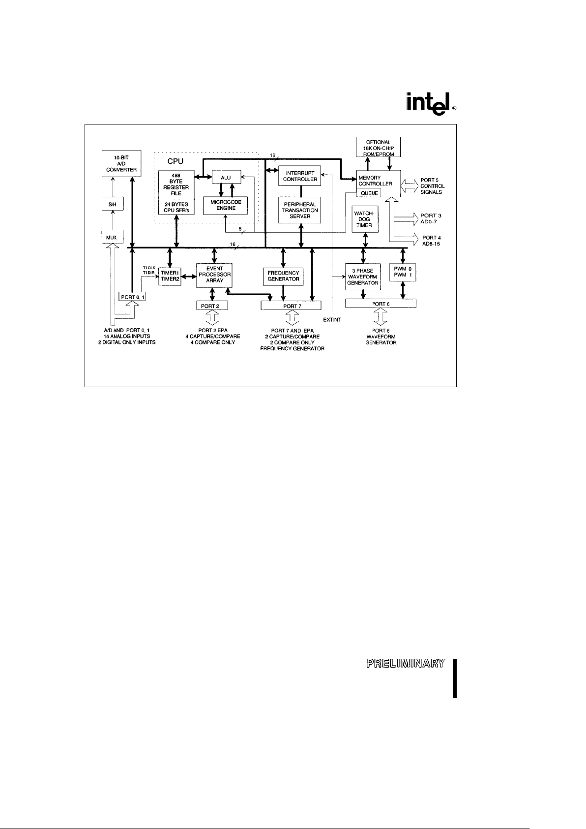
8XC196MD
272323– 1
NOTE:
Connections between the standard I/O ports and the bus are not shown.
Figure 1. 87C196MD Block Diagram
2
8XC196MD
PROCESS INFORMATION
This device is manufactured on PX29.5, a CHMOS
III-E process. Additional process and reliability information is available in Intel’s
Components Quality
and Reliability Handbook,
Order Number 210997.
272323– 2
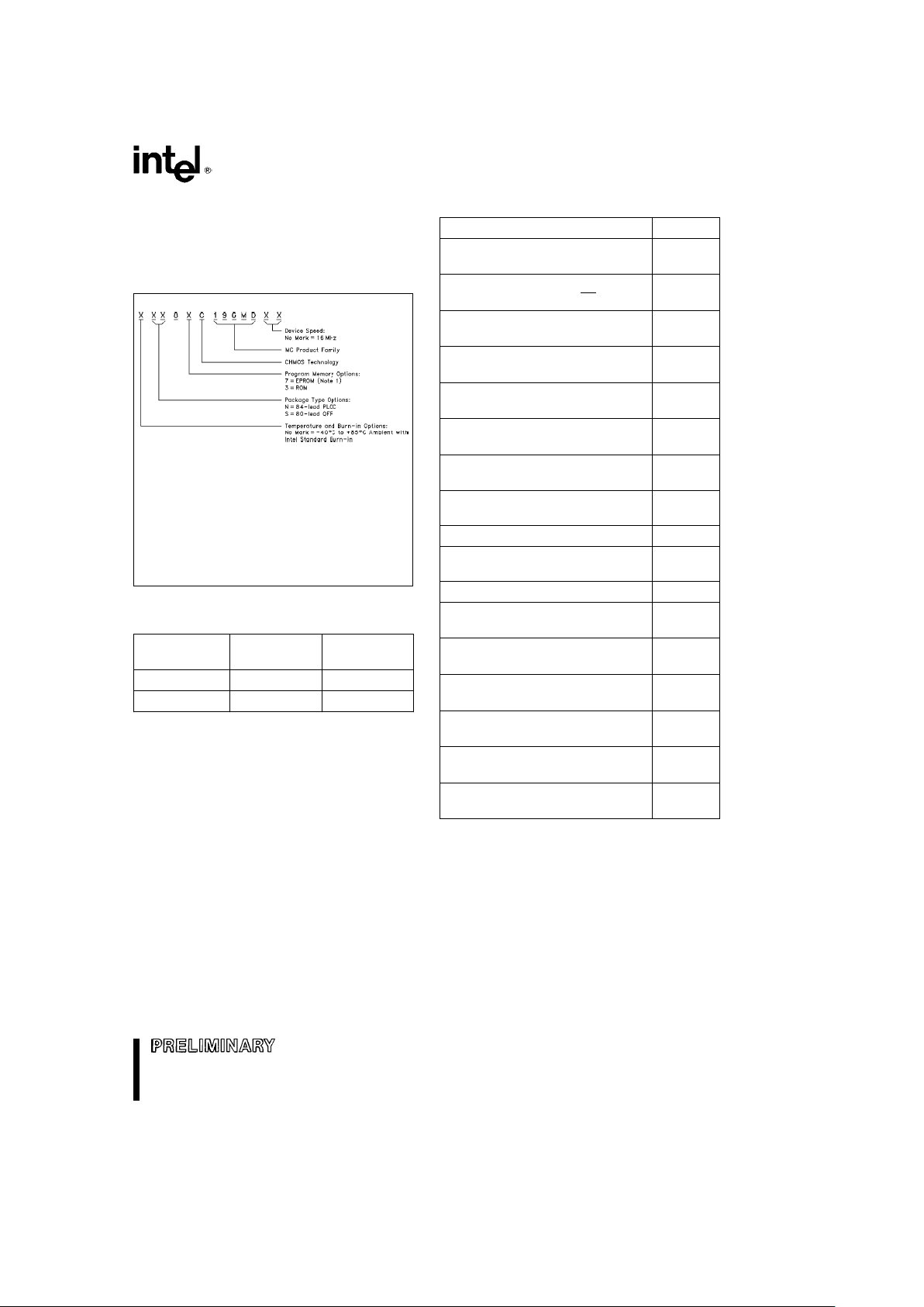
EXAMPLE: N87C196MD is 84-Lead PLCC OTPROM,
16 MHz.
For complete package dimensional data, refer to the
Intel Packaging Handbook (Order Number 240800).
NOTE:
EPROMs are available as One Time Programmable
(OTPROM) only.
Figure 2. The 8XC196MD Family Nomenclature
Table 1. Thermal Characteristics
Package
i
ja
i
jc
Type
PLCC 35§C/W 13§C/W
QFP 56§C/W 12§C/W
All thermal impedance data is approximate for static air
conditions at 1W of power dissipation. Values will change
depending on operation conditions and application. See
the Intel
Packaging Handbook
(order number 240800) for a
description of Intel’s thermal impedance test methodology.
Table 2. 8XC196MD Memory Map
Description Address
External Memory or I/O 0FFFFH
06000H
Internal ROM/EPROM or External 5FFFH
Memory (Determined by EA
)
2080H
Reserved. Must contain FFH. 207FH
(Note 5)
205EH
PTS Vectors 205DH
2040H
Upper Interrupt Vectors 203FH
2030H
ROM/EPROM Security Key 202FH
2020H
Reserved. Must contain FFH. 201FH
(Note 5)
201CH
Reserved. Must Contain 20H 201BH
(Note 5)
CCB1 201AH
Reserved. Must Contain 20H 2019H
(Note 5)
CCB0 2018H
Reserved. Must contain FFH. 2017H
(Note 5)
2014H
Lower Interrupt Vectors 2013H
2000H
SFR’s 1FFFH
1F00H
External Memory 1EFFH
0200H
488 Bytes Register RAM (Note 1) 01FFH
0018H
CPU SFR’s (Notes 1, 3) 0017H
0000H
NOTES:
1. Code executed in locations 0000H to 01FFH will be
forced external.
2. Reserved memory locations must contain 0FFH unless
noted.
3. Reserved SFR bit locations must contain 0.
4. Refer to 8XC196MC for SFR descriptions.
5. WARNING: Reserved memory locations must not be
written or read. The contents and/or function of these locations may change with future revisions of the device.
Therefore, a program that relies on one or more of these
locations may not function properly.
3
8XC196MD
8XC196MC AND 8XC196MD
DIFFERENCES
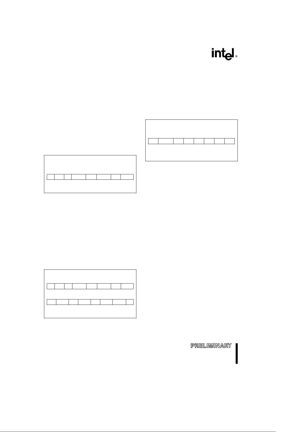
INTÐMASK1/INTÐPEND1 Registers
There are some differences between the
8XC196MC and 8XC196MD INTÐMASK1/
INTÐPEND1 registers. The 8XC196MD interrupt
mask and pending registers are shown below. Notice that the CAPCOM5, COMP4, and CAPCOM4
bits are reserved bits on the 8XC196MC. The PI bit
of the INTÐPEND1 register will be set when a
Waveform Generator or Compare Module 5 event
occurs and the corresponding bit in the PIÐMASK
register is set. The PI interrupt vector can be taken
when the PI bit in the INTÐMASK1 register is set.
The 8XC196MC User’s Manual should be referenced for details about the interrupts.
INTÐMASK1 (0031H)
and INTÐPEND1 (0012H)
765 4 3 2 1 0
RSV EXTINT PI CAPCOM5* COMP4* CAPCOM4* COMP3 CAPCOM3
RSVeRESERVED BIT. MUST WRITE AS 0
*
e
THIS BIT RESERVED ON 8XC196MC.
Figure 3. Interrupt Mask and Status Registers
PTSSRV and PTSSEL Register
Similarly, there are differences between 8XC196MC
and 8XC196MD PTS registers. The 8XC196MD PTS
registers are shown below. Notice the CAPCOM5,
COMP4, and CAPCOM4 bits are reserved bits on
the 8XC196MC. The PI bit in the PTSSRV will be set
when a Waveform Generator or Compare Module 5
end of PTS interrupt occurs and the corresponding
bit in the PIÐMASK register is set. The PI PTS vector can be used when the PI bit in the PTSSEL register is set. The 8XC196MC User’s Manual should be
referenced for details about the PTS.
PTSSEL (0004H) and PTSSRV (0006H)
15 14 13 12 11 10 9 8
RSV EXTINT PI CAPCOM5* COMP4* CAPCOM4* COMP3 CAPCOM3
765432 10
COMP2 CAPCOM2 COMP1 CAPCOM1 COMP0 CAPCOM0 ADÐDONE TOVF
RSVeRESERVED BIT. MUST WRITE AS 0
*
e
THIS BIT RESERVED ON 8XC196MC.
Figure 4. PTS Select and Service Registers
PIÐMASK and PIÐPEND Registers
The PIÐMASK/PIÐPEND registers contain the bits
for the Compare Module 5 (COMP5) Waveform Generator (WG), Timer 1 Overflow (TFI), and Timer 2
Overflow (TF2) mask/status flag. The diagram below shows the registers. Notice that the COMP5 bit
is a reserved bit on the 8XC196MC. The 8XC196MC
User’s Manual should be referenced for details
about the Waveform Generator, Compare Modules,
and Timers.
PIÐMASK (1FBEH) and
PIÐPEND (1FBCH, Read Only)
7 6 543210
RSV COMP5* RSV WG RSV TF2 RSV TF1
RSVeRESERVED BIT. MUST WRITE AS 0,
READ AS 1.
*eTHIS BIT RESERVED ON 8XC196MC.
Figure 5. Peripheral Interrupt Mask
and Status Registers
The PI bit in the INTÐPEND1 register is set if a
Waveform Generator event or Compare Module 5
event occurs and the corresponding PIÐMASK bit is
set. For either of these events to cause an interrupt,
the PI bit in the INTÐMASK1 register and the corresponding event bit in the PIÐMASK register must be
set.
Similarly, the TOVF bit in the INTÐPEND register is
set if Timer 1 or Timer 2 overflow and the corresponding bit in the PIÐMASK register is set. For either of these two events to cause an interrupt, the
TOVF bit in the INTÐMASK register and the corresponding event bit in the PIÐMASK must be set.
Upon a PI and/or a TOVF interrupt, it may be necessary to check if the Compare Module 5, the Waveform Generator, Timer 1, or Timer 2 event caused
the interrupt. The PIÐPEND will give this information. However, it should be noted that reading the
PIÐPEND register will clear the register. So the individual bits in the PIÐPEND register must be read by
loading PIÐPEND into another ‘‘shadow’’ register,
then checking the ‘‘shadow’’ register to see what
event occurred.
4
8XC196MD
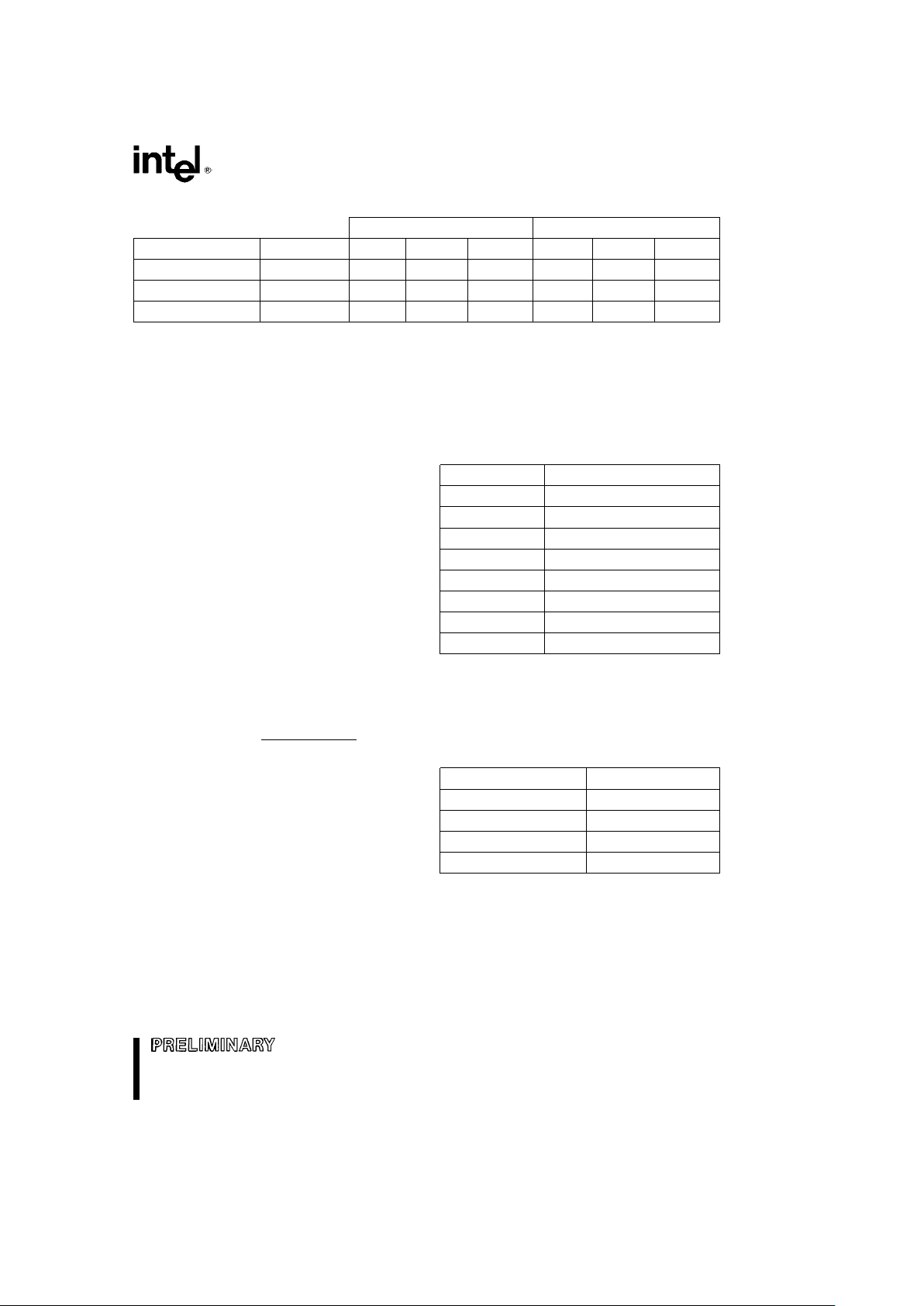
Table 3. Interrupt Sources, Vectors and Priorities
Interrupt Service PTS Service
Interrupt Source Symbol Name Vector Priority Name Vector Priority
Capture/Compare5 CAPCOMP5 INT12 2038H 12 PTS12 2058H 27
Compare4 COMP4 INT11 2036H 11 PTS11 2056H 26
Capture/Compare4 CAPCOMP4 INT10 2034H 10 PTS10 2054H 25
Interrupt and PTS Vectors
The 8XC196MD has three new interrupt and PTS
vectors which are Capture/Compare5, Compare 4,
and Capture/Compare4. Table 3 shows these interrupt vectors and priorities. These are shown as reserved vectors in the 8XC196MC User’s Manual.
Frequency Generator
The Frequency Generator (FG) Peripheral which
was not available on the 8XC196MC device, is available on the 8XC196MD device. The FG outputs a
programmable-frequency 50% duty cycle waveform
on the FREQOUT pin (P7.7). There are two 8-bit registers which control the FG peripheral:
Ð Frequency Generator Control Register
(FGÐCON) at 1FB8h
Ð Frequency Generator Period Count Register
(FGÐCOUNT) at 1FBAh.
The FGÐCON can be read or written. This register
is loaded with a value which determines the number
of counts necessary for toggling the output. The following equation should be used to calculate the
FGÐCON value:
FGÐCON value
e
F
XTAL
16 * (FG Frequency)
b
1
where FG Frequency is from 4 kHz to 1 MHz.
The FGÐCOUNT is loaded with the FGÐCON register value. The FGÐCOUNT register is decremented every eighth state time. When it reaches 00h, the
FGÐCOUNT register will send a signal to toggle the
output pin and reload the FGÐCOUNT register with
the value in the FGÐCON register. The
FGÐCOUNT can only be read, not written.
The FREQOUT pin (P7.7) must be configured for a
special function to use it for the Frequency Generator feature.
Port 7
Port 7 is an additional bidirectional port that was not
available on the 8XC196MC device. Port 7 can be
used as I/O or some of the pins have special functions. The pins are listed below followed by their
special functions.
Table 4. Port 7 Special Function Pins
Pin Special Function
P7.0 CAPCOMP4
P7.1 CAPCOMP5
P7.2 CAPCOMP4
P7.3 CAPCOMP5
P7.4
P7.5
P7.6
P7.7 FREQOUT
The special functions of the pins are selected in the
Port 7 SFRs. The Port 2 I/O Port section of the
8XC196MC User’s Manual can be referenced when
setting up the Port 7 SFRs. Port 7 SFRs are located
in the following locations:
Table 5. Port 7 Special Function Registers
SFR Address
P7ÐMODE 1FD1h
P7ÐDIR 1FD3h
P7ÐREG 1FD5h
P7ÐPIN 1FD7h
5

8XC196MD
Port 1
There are three additional Port 1 input pins (P1.5–
P1.7) that were not available on the 8XC196MC.
These pins are listed below followed by their function:
Table 6. New 8XC196MD Port 1 Pins
Pin Description
P1.5 Digital or Analog Input
P1.6 Digital Input
P1.7 Digital Input
NOTE:
P1.5 was a V
SS
pin on the 8XC196MC device. If
P1.5 and P1.6 are not being used these pins can
remain connected to V
SS
.
6
8XC196MD
272323– 3
NOTE:
NC means No Connect. Do not connect these pins.
Figure 6. 84-Lead PLCC Package
7
8XC196MD
272323– 4
Figure 7. 80-Lead Shrink EIAJQFP (Quad Flat Pack)
8
 Loading...