*Other brands and names are the property of their respective owners.
Information in this document is provided in connection with Intel products. Intel assumes no liability whatsoever, including infringement of any patent or
copyright, for sale and use of Intel products except as provided in Intel’s Terms and Conditions of Sale for such products. Intel retains the right to make
changes to these specifications at any time, without notice. Microcomputer Products may have minor variations to this specification known as errata.
October 1992COPYRIGHT©INTEL CORPORATION, 1995 Order Number: 272034-003
8XC198
COMMERCIAL/EXPRESS CHMOS MICROCONTROLLER
8 Kbytes of OTPROM
Y
8 Kbytes of On-Chip OTPROM or ROM
Y
232 Byte Register File
Y
Register-to-Register Architecture
Y
28 Interrupt Sources/16 Vectors
Y
1.75 ms 16 x 16 Multiply (16 MHz)
Y
3.0 ms 32/16 Divide (16 MHz)
Y
Powerdown and Idle Modes
Y
16-Bit Watchdog Timer
Y
8-Bit External Bus
Y
16 MHz Standard
Y
Full Duplex Serial Port
Y
High Speed I/O Subsystem
Y
16-Bit Timer
Y
16-Bit Counter
Y
Pulse-Width-Modulated Output
Y
Four 16-Bit Software Timers
Y
10-Bit A/D Converter with Sample/Hold
Y
Extended Temperature Available
The 8XC198 family offers low-cost entry into Intel’s powerful MCSÉ-96 16-bit microcontroller architecture.
Intel’s CHMOS process provides a high performance processor along with low power consumption. To further
reduce power requirements, the processor can be placed into Idle or Powerdown Mode.
The 8XC198 is the 8-bit bus version of the 8XC196KB. The prefixes mean: 80 (ROMless), 83 (ROM), 87 (OTP)
One Time Programmable. The ROM and OTP are available in 8 Kbytes.
Bit, byte, word and some 32-bit operations are available on the 8XC198. With a 16 MHz oscillator a 16-bit
addition takes 0.50 ms, and the instruction times average 0.37 ms to 1.1 ms in typical applications.
Four high-speed capture inputs are provided to record times when events occur. Six high-speed outputs are
available for pulse or waveform generation. The high-speed output can also generate four software timers or
start an A/D conversion. Events can be based on the timer or counter. Also provided on-chip are an A/D
converter, serial port, watchdog timer and a pulse-width-modulated output signal.
With the commercial (standard) temperature option, operational characteristics are guaranteed over the temperature range of 0
§
Ctoa70§C. Wth the extended temperature range option, operational characteristics are
guaranteed over the temperature range of
b
40§Ctoa85§C.
MCSÉ-96 is a registered trademark of Intel Corporation.

8XC198
272034– 1
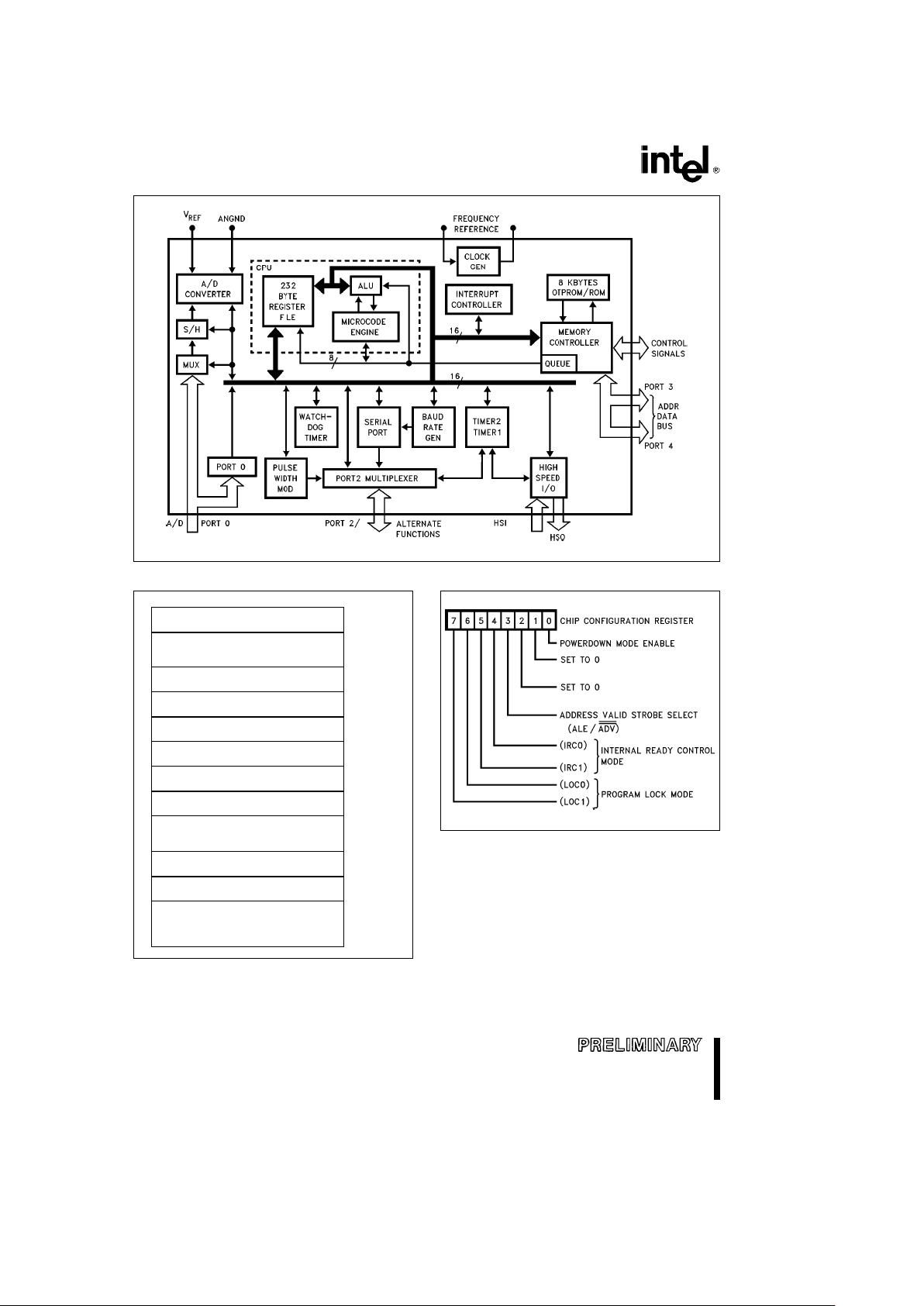
Figure 1. 87C198 Block Diagram
EXTERNAL MEMORY OR I/O
0FFFFH
4000H
INTERNAL ROM/E PROM OR
EXTERNAL MEMORY
2080H
RESERVED
2040H
UPPER 8 INTERRUPT VECTORS
2030H
ROM/OTP SECURITY KEY
2020H
RESERVED
2019H
CHIP CONFIGURATION BYTE
2018H
RESERVED
2014H
LOWER 8 INTERRUPT VECTORS
PLUS 2 SPECIAL INTERRUPTS
2000H
PORT 3 AND PORT 4
1FFEH
EXTERNAL MEMORY OR I/O
0100H
INTERNAL DATA MEMORY - REGISTER FILE
(STACK POINTER, RAM AND SFRS)
EXTERNAL PROGRAM CODE MEMORY
0000H
Figure 2. Memory Map
272034– 7
Figure 3. Chip Configuration (2018H)
WARNING:
Reserved memory locations must not be written or read. The contents and/or function of these locations may change with
future revisions of the device. Therefore, a program that relies on one or more of these locations may not function properly.
2

8XC198
PACKAGING
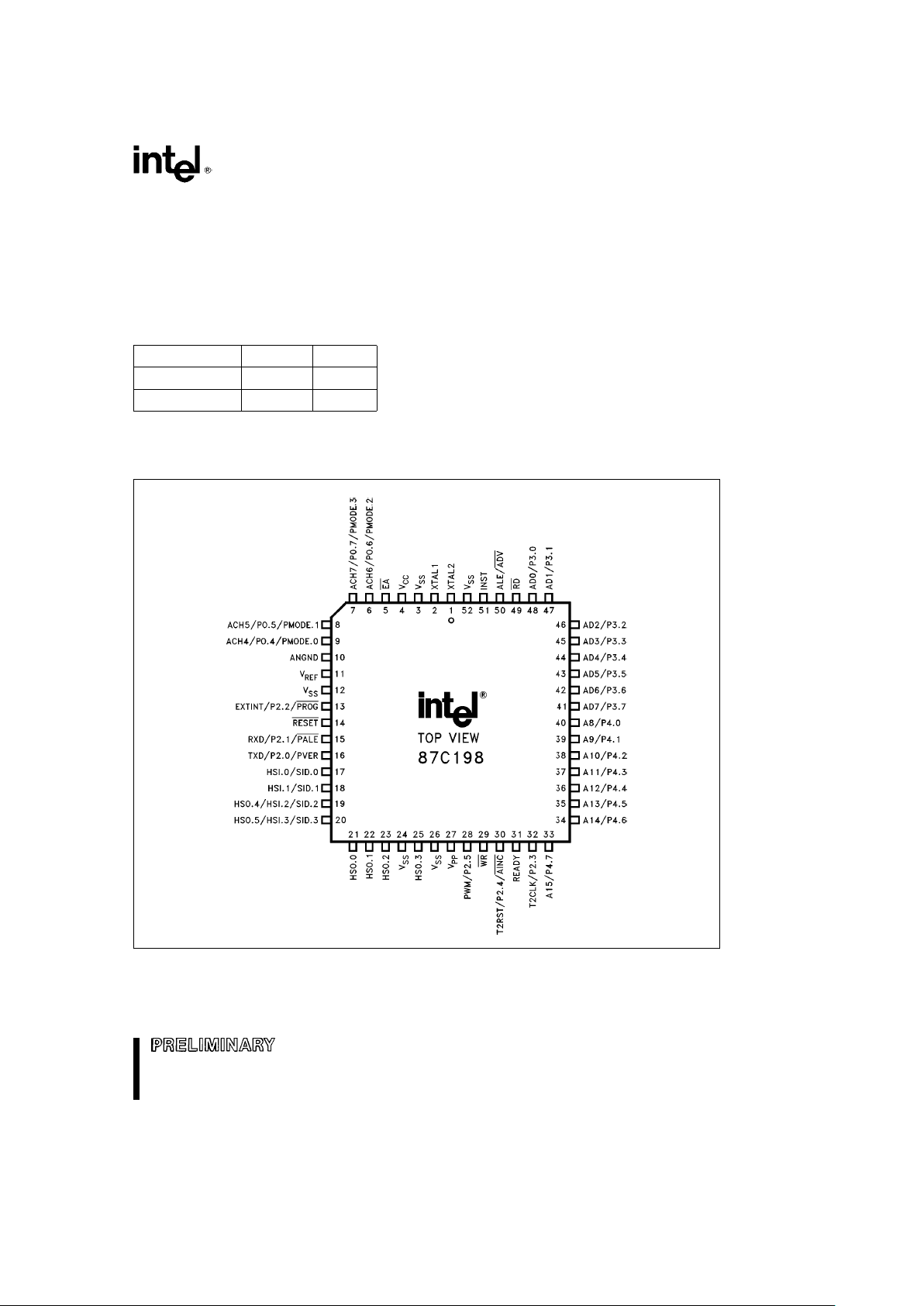
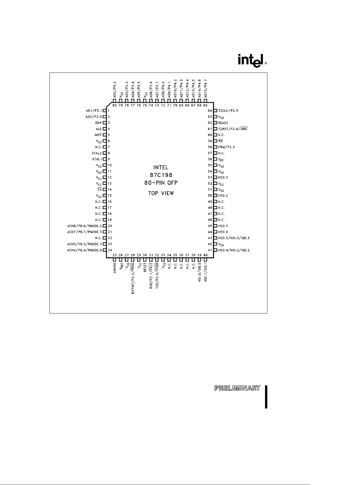
The 8XC198 is available in a 52-pin PLCC package and an 80-pin QFP package. Contact your local sales
office to determine the exact ordering code for the part desired.
Package Designators:
N
e
52-pin PLCC
S
e
80-pin QFP
Thermal Characteristics
Package Type i
ja
i
jc
PLCC 40§C/W
QFP 70§C/W 4§C/W
All thermal impedance data is approximate for static air conditions at 1W of power dissipation. Values will
change depending on operating conditions and application. See the Intel
Packaging Handbook
(Order Number
240800) for a description of Intel’s thermal impedance test methodology.
272034– 2
Figure 4. 52-Pin PLCC Package
NOTE:
The above pinout diagram applies to the OTP (87C198) device. The OTP device uses all of the programming pins shown
above. The ROM (83C198) device only uses programming pins: AINC, PALE, PMODE.n and PROG. The ROMless (80C198)
doesn’t use any of the programming pins.
3

8XC198
272034– 4
NOTE:
N.C. means No Connect (do not connect these pins).
Figure 5. 80-Pin QFP Package
NOTE:
The above pinout diagram applies to the OTP (87C198) device. The OTP device uses all of the programming pins shown
above. The ROM (83C198) device only uses programming pins: AINC, PALE, PMODE.n and PROG. The ROMless (80C198)
doesn’t use any of the programming pins.
4

8XC198
PIN DESCRIPTIONS
Symbol Name and Function
V
CC
Main supply voltage (5V).
V
SS
The PLCC package has 5 VSSpins and the QFP package has 12 VSSpins. All must be
connected to digital ground.
V
REF
Reference voltage for the A/D converter (5V). V
REF
is also the supply voltage to the
analog portion of the A/D converter and the logic used to read Port 0. Must be
connected for A/D and Port 0 to function.
ANGND Reference ground for the A/D converter. Must be held at nominally the same potential
as V
SS
.
V
PP
Programming Voltage. Also, timing pin for the return from powerdown circuit.
XTAL1 Input of the oscillator inverter and of the internal clock generator.
XTAL2 Output of the oscillator inverter.
RESET Reset input to and open-drain output from the chip. Input low for at least 4 state times to
reset the chip. The subsequent low-to-high transition commences the 10-state Reset
Sequence.
INST Output high during an external memory read indicates the read is an instruction fetch.
INST is valid throughout the bus cycle. INST is activated only during external memory
accesses and output low for a data fetch.
EA Input for memory select (External Access). EA equal to a TTL-high causes memory
accesses to locations 2000H through 3FFFH to be directed to on-chip ROM/EPROM.
EA
equal to a TTL-low causes accesses to these locations to be directed to off-chip
memory.
ALE/ADV Address Latch Enable or Address Valid output, as selected by CCR. Both pin options
provide a latch to demultiplex the address from the address/data bus. When the pin is
ADV
, it goes inactive high at the end of the bus cycle. ALE/ADV is activated only during
external memory accesses.
RD Read signal output to external memory. RD is activated only during external memory
reads.
WR Write output to external memory. WR will go low for every external write.
READY Ready input to lengthen external memory cycles. When the external memory is not
being used, READY has no effect. Internal control of the number of wait states inserted
into a bus cycle held not ready is available through configuration of CCR.
HSI Inputs to High Speed Input Unit. Four HSI pins are available: HSI.0, HSI.1, HSI.2 and
HSI.3. Two of them (HSI.2 and HSI.3) are shared with the HSO Unit.
HSO Outputs from High Speed Output Unit. Six HSO pins are available: HSO.0, HSO.1,
HSO.2, HSO.3, HSO.4 and HSO.5. Two of them (HSO.4 and HSO.5) are shared with the
HSI Unit.
Port 0 4-bit high impedance input-only port. These pins can be used as digital inputs and/or as
analog inputs to the on-chip A/D converter. These pins set the Programming Mode on
the EPROM device.
5

8XC198
PIN DESCRIPTIONS (Continued)
Symbol Name and Function
Port 2 Multi-functional port. All of its pins are shared with other functions in the 80C198.
Ports 3 and 4 8-bit bidirectional I/O ports with open drain outputs. These pins are shared with
the multiplexed address/data bus which has strong internal pullups. Available as
I/O only on the ROM and EPROM devices.
TxD The TxD pin is used for serial port transmission in Modes 1, 2 and 3. In mode 0 the
pin is used as the serial clock output.
RxD Serial Port Receive pin used for serial port reception. In mode 0 the pin functions
as input or output data.
EXTINT A positive transition on the EXTINT pin will generate an external interrupt.
T2CLK The T2CLK pin is the Timer2 clock input or the serial port baud rate generator
input.
T2RST A rising edge on the T2RST pin will reset Timer2.
PWM The PWM output.
PMODE Programming Mode Select. Determines the EPROM programming algorithm that is
performed. PMODE is sampled after a chip reset and should be static while the
part is operating.
SID Slave ID Number. Used to assign each slave a pin of Port 3 or 4 to use for passing
programming verification acknowledgement.
PALE Programming ALE Input. Accepted by the 87C196KB when it is in Slave
Programming Mode. Used to indicate that Ports 3 and 4 contain a command/
address.
PROG Programming. Falling edge indicates valid data on PBUS and the beginning of
programming. Rising edge indicates end of programming.
PVAL Program Valid. This signal indicates the success or failure of programming in the
Auto Programming Mode. A zero indicates successful programming.
PVER Program Verification. Used in Slave Programming and Auto CLB Programming
Modes. Signal is low after rising edge of PROG if the programming was not
successful.
AINC Auto Increment. Active low signal indicates that the auto increment mode is
enabled. Auto Increment will allow reading or writing of sequential EPROM
locations without address transactions across the PBUS for each read or write.
PORTS 3 and 4 Address/Command/Data Bus. Used to pass commands, addresses, and data to
and from slave mode 87C196KBs. Used by chips in Auto Programming Mode to
(when programming)
pass command, addresses and data to slaves. Also used in the Auto Programming
Mode as a regular system bus to access external memory. Should have pullups to
VCC(15 kX).
6
 Loading...