Intel Corporation N82C42PC, N82C42PD, N80L42, N87C42, P80C42 Datasheet
...
UPI-C42/UPI-L42
UNIVERSAL PERIPHERAL INTERFACE
CHMOS 8-BIT SLAVE MICROCONTROLLER
Y
Pin, Software and Architecturally
Compatible with all UPI-41 and UPI-42
Products
Y
Low Voltage Operation with the UPIL42
Ð Full 3.3V Support
Y
Hardware A20 Gate Support
Y
Suspend Power Down Mode
Y
Security Bit Code Protection Support
Y
8-Bit CPU plus ROM/OTP EPROM, RAM,
I/O, Timer/Counter and Clock in a
Single Package
Y
4096 x 8 ROM/OTP, 256 x 8 RAM 8-Bit
Timer/Counter, 18 Programmable I/O
Pins
Y
DMA, Interrupt, or Polled Operation
Supported
The UPI-C42 is an enhanced CHMOS version of the industry standard Intel UPI-42 family. It is fabricated on
Intel’s CHMOS III-E process. The UPI-C42 is pin, software, and architecturally compatible with the NMOS UPI
family. The UPI-C42 has all of the same features of the NMOS family plus a larger user programmable memory
array (4K), hardware A20 gate support, and lower power consumption inherent to a CHMOS product.
The UPI-L42 offers the same functionality and socket compatibility as the UPI-C42 as well as providing low
voltage 3.3V operation.
The UPI-C42 is essentially a ‘‘slave’’ microcontroller, or a microcontroller with a slave interface included on the
chip. Interface registers are included to enable the UPI device to function as a slave peripheral controller in the
MCS Modules and iAPX family, as well as other 8-, 16-, and 32-bit systems.
To allow full user flexibility, the program memory is available in ROM and One-Time Programmable EPROM
(OTP).
Y
One 8-Bit Status and Two Data
Registers for Asynchronous Slave-toMaster Interface
Y
Fully Compatible with all Intel and Most
Other Microprocessor Families
Y
Interchangeable ROM and OTP EPROM
Versions
Y
Expandable I/O
Y
Sync Mode Available
Y
Over 90 Instructions: 70% Single Byte
Y
Quick Pulse Programming Algorithm
Ð Fast OTP Programming
Y
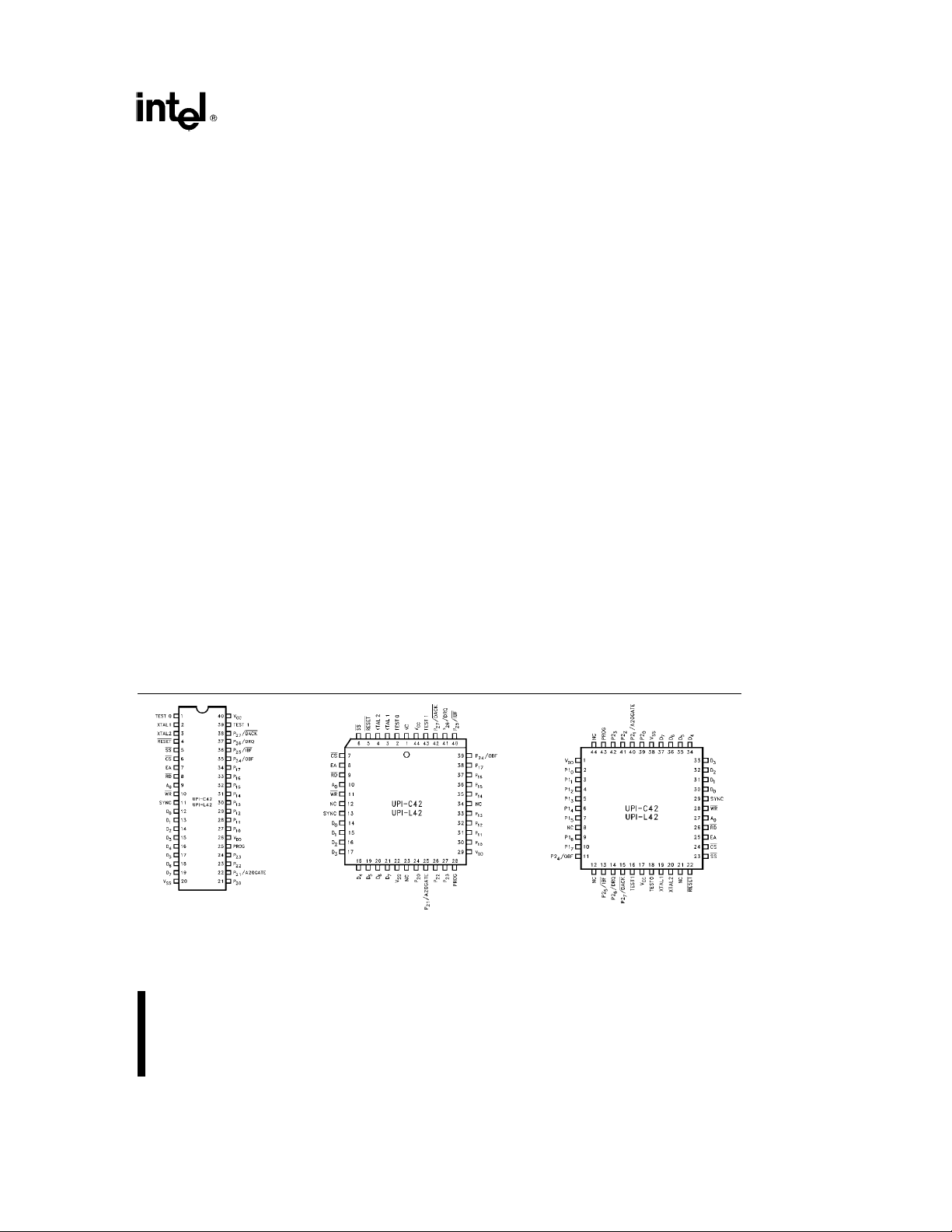
Available in 40-Lead Plastic, 44-Lead
Plastic Leaded Chip Carrier, and
44-Lead Quad Flat Pack Packages
(See Packaging Spec., OrderÝ240800, Package Type P, N,
and S)
Figure 1. DIP Pin
Configuration
*Other brands and names are the property of their respective owners.
Information in this document is provided in connection with Intel products. Intel assumes no liability whatsoever, including infringement of any patent or
copyright, for sale and use of Intel products except as provided in Intel’s Terms and Conditions of Sale for such products. Intel retains the right to make
changes to these specifications at any time, without notice. Microcomputer Products may have minor variations to this specification known as errata.
290414– 1
Figure 2. PLCC Pin Configuration
290414– 2
December 1995COPYRIGHT©INTEL CORPORATION, 1996 Order Number: 290414-003
Figure 3. QFP Pin Configuration
290414– 3

UPI-C42/UPI-L42
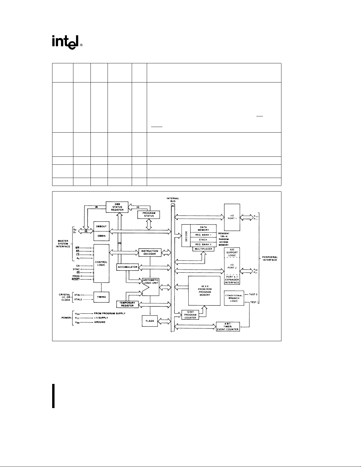
Table 1. Pin Description
Symbol Pin Pin Pin Type Name and Function
TEST 0, 1 2 18 I TEST INPUTS: Input pins which can be directly tested using conditional
TEST 1 39 43 16
XTAL 1 2 3 19 O OUTPUT: Output from the oscillator amplifier.
XTAL 2 3 4 20 I INPUT: Input to the oscillator amplifier and internal clock generator
RESET 4 5 22 I RESET: Input used to reset status flip-flops, set the program counter to
SS 5 6 23 I SINGLE STEP: Single step input used in conjunction with the SYNC output
CS 6 7 24 I CHIP SELECT: Chip select input used to select one UPI microcomputer
EA 7 8 25 I EXTERNAL ACCESS: External access input which allows emulation,
RD 8 9 26 I READ: I/O read input which enables the master CPU to read data and
A
0
WR 10 11 28 I WRITE: I/O write input which enables the master CPU to write data and
SYNC 11 13 29 O OUTPUT CLOCK: Output signal which occurs once per UPI instruction
D0–D
(BUS)
P10–P1727–34 30–33 2–10 I/O PORT 1: 8-bit, PORT 1 quasi-bidirectional I/O lines. P10–P17access the
DIP PLCC QFP
No. No. No.
branch instructions.
FREQUENCY REFERENCE: TEST 1 (T
input (under software control). TEST 0 (T
during PROM programming and ROM/EPROM verification, during Sync
) functions as the event timer
1
) is a multi-function pin used
0
Mode to reset the instruction state to S1 and synchronize the internal clock
to PH1.
circuits.
zero, and force the UPI-C42 from the suspend power down mode.
is also used during EPROM programming and verification.
RESET
to step the program through each instruction (EPROM). This should be tied
a
5V when not used. This pin is also used to put the device in Sync
to
Mode by applying 12.5V to it.
out of several connected to a common data bus.
testing and ROM/EPROM verification. This pin should be tied low if
unused.
status words from the OUTPUT DATA BUS BUFFER or status register.
91027ICOMMAND/DATA SELECT: Address Input used by the master processor
e
to indicate whether byte transfer is data (A
e
(A
0
1, F1 is set). A
e
0 during program and verify operations.
0
0, F1 is reset) or command
0
command words to the UPI INPUT DATA BUS BUFFER.
cycle. SYNC can be used as a strobe for external circuitry; it is also used to
synchronize single step operation.
12–19 14–21 30–37 I/O DATA BUS: Three-state, bidirectional DATA BUS BUFFER lines used to
7
35–38
interface the UPI microcomputer to an 8-bit master system data bus.
signature row and security bit.
2
UPI-C42/UPI-L42
Table 1. Pin Description (Continued)
Symbol Pin Pin Pin Type Name and Function
P20–P2721–24 24–27 39–42 I/O PORT 2: 8-bit, PORT 2 quasi-bidirectional I/O lines. The lower 4 bits
PROG 25 28 43 I/O PROGRAM: Multifunction pin used as the program pulse input during
V
CC
V
DD
V
SS
DIP PLCC QFP
No. No. No.
) interface directly to the 8243 I/O expander device and
35–38 39–42 11,13–15
(P
20–P23
contain address and data information during PORT 4 – 7 access. P
can be programmed to provide hardware A20 gate support. The upper
4 bits (P24–P27) can be programmed to provide interrupt Request and
DMA Handshake capability. Software control can configure P
Output Buffer Full (OBF) interrupt, P
interrupt, P
(DACK
as DMA Request (DRQ), and P27as DMA ACKnowledge
26
).
as Input Buffer Full (IBF)
25
24
PROM programming.
During I/O expander access the PROG pin acts as an address/data
strobe to the 8243. This pin should be tied high if unused.
40 44 17 POWER:a5V main power supply pin.
26 29 1 POWER:a5V during normal operation.a12.75V during programming
operation. Low power standby supply pin.
20 22 38 GROUND: Circuit ground potential.
21
as
Figure 4. Block Diagram
290414– 4
3
UPI-C42/UPI-L42
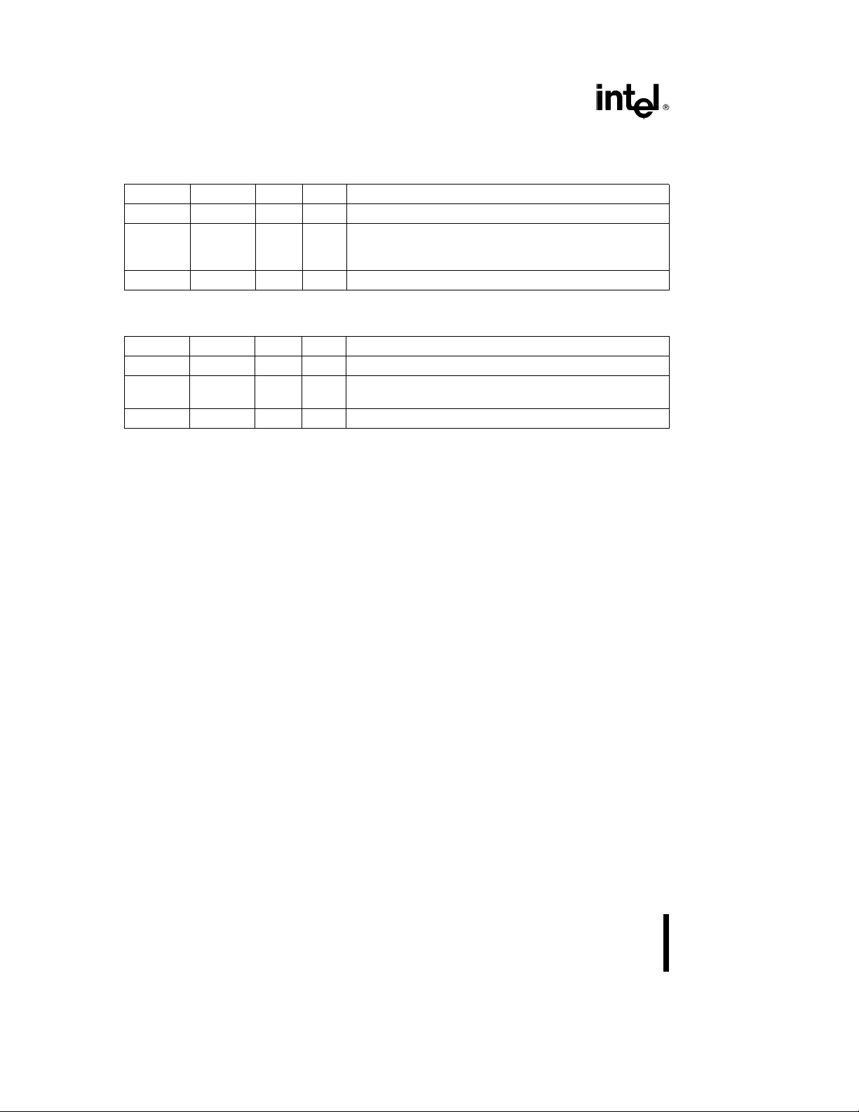
UPI-C42/L42 PRODUCT SELECTION GUIDE
UPI-C42: Low power CHMOS version of the UPI-42.
Device Package ROM OTP Comments
80C42 N, P S 4K ROM Device
82C42PC N, P, S Phoenix MultiKey/42 firmware, PS/2 style mouse support
82C42PD N, P, S Phoenix MultiKey/42L firmware, KBC and SCC for portable apps.
82C42PE N, P, S Phoenix MultiKey/42G firmware, Energy Efficient KBC solution
87C42 N, P, S 4K One Time Programmable Version
UPI-L42: The low voltage 3.3V version of the UPI-C42.
Device Package ROM OTP Comments
80L42 N, P S 4K ROM Device
82L42PC N, P, S Phoenix MultiKey/42 firmware, PS/2 style mouse support
82L42PD N, P, S Phoenix MultiKey/42L firmware, KBC and SCC for portable apps.
87L42 N, P, S 4K One Time Programmable Version
Ne44 lead PLCC, Pe40 lead PDIP, Se44 lead QFP, De40 lead CERDIP
e
Key Board Control, SCCeScan Code Control
KBC
THE INTEL 82C42
As shown in the UPI-C42 product matrix, the UPIC42 is offered as a pre-programmed 80C42 with various versions of MultiKey/42 keyboard controller
firmware developed by Phoenix Technologies Ltd.
The 82C42PC provides a low powered solution for
industry standard keyboard and PS/2 style mouse
control. The 82C42PD provides a cost effective
means for keyboard and scan code control for notebook platforms. The 82C42PE allows a quick time to
market, low cost solution for energy efficient desktop designs.
4
UPI-C42/UPI-L42
UPI-42 COMPATIBLE FEATURES
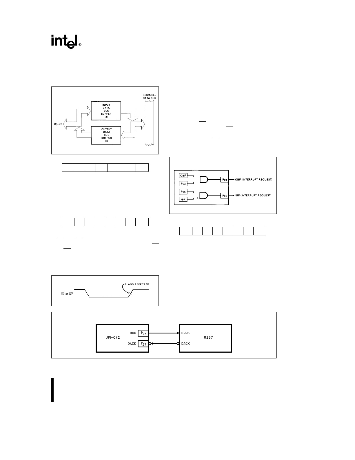
1. Two Data Bus Buffers, one for input and one for
output. This allows a much cleaner Master/Slave
protocol.
290414– 5
2. 8 Bits of Status
ST7ST6ST5ST4F1F0IBF OBF
D7D6D5D4D3D2D1D
ST4–ST7are user definable status bits. These
bits are defined by the ‘‘MOV STS, A’’ single
byte, single cycle instruction. Bits 4 – 7 of the
acccumulator are moved to bits 4–7 of the status
register. Bits 0 – 3 of the status register are not
affected.
MOV STS, A Op Code: 90H
1 001000 0
D
7
3. RD and WR are edge triggered. IBF, OBF, F1and
INT change internally after the trailing edge of RD
or WR.
During the time that the host CPU is reading the
status register, the UPI is prevented from updating this register or is ‘locked out.’
0
D
0
290414– 6
4. P24and P25are port pins or Buffer Flag pins
which can be used to interrupt a master processor. These pins default to port pins on Reset.
If the ‘‘EN FLAGS’’ instruction has been executed, P
pin. A ‘‘1’’ written to P
pin outputs the OBF Status Bit). A ‘‘0’’ written to
P
This pin can be used to indicate that valid data is
becomes the OBF (Output Buffer Full)
24
disables the OBF pin (the pin remains low).
24
enables the OBF pin (the
24
available from the UPI (in Output Data Bus Buffer).
If ‘‘EN FLAGS’’ has been executed, P
comes the IBF
ten to P
the inverse of the IBF Status Bit. A ‘‘0’’ written to
disables the IBF pin (the pin remains low).
P
25
This pin can be used to indicate that the UPI is
(Input Buffer Full) pin. A ‘‘1’’ writ-
enables the IBF pin (the pin outputs
25
be-
25
ready for data.
Data Bus Buffer Interrupt Capability
290414– 7
EN FLAGS Op Code: 0F5H
1 111010 1
D
7
D
0
5. P26and P27are port pins or DMA handshake
pins for use with a DMA controller. These pins
default to port pins on Reset.
If the ‘‘EN DMA’’ instruction has been executed,
P
becomes the DRQ (DMA Request) pin. A ‘‘1’’
26
written to P
activated). DRQ is deactivated by DACK
DACK
#
causes a DMA request (DRQ is
26
#
RD,
WR, or execution of the ‘‘EN DMA’’ in-
struction.
DMA Handshake Capability
290414– 8
5
UPI-C42/UPI-L42
If ‘‘EN DMA’’ has been executed, P27becomes
the DACK
as a chip select input for the Data Bus Buffer
registers during DMA transfers.
EN DMA Op Code: 0E5H
6. When EA is enabled on the UPI, the program
counter is placed on Port 1 and the lower four
bits of Port 2 (MSB
UPI this information is multiplexed with PORT
DATA (see port timing diagrams at end of this
data sheet).
7. The UPI-C42 supports the Quick Pulse Programming Algorithm, but can also be programmed
with the Intelligent Programming Algorithm. (See
the Programming Section.)
(DMA ACKnowledge) pin. This pin acts
1 110010 1
D
7
e
P23, LSBeP10). On the
D
0
UPI-C42 FEATURES
Programmable Memory Size Increase
The user programmable memory on the UPI-C42 will
be increased from the 2K available in the NMOS
product by 2X to 4K. The larger user programmable
memory array will allow the user to develop more
complex peripheral control micro-code. P2.3 (port 2
bit 3) has been designated as the extra address pin
required to support the programming of the extra 2K
of user programmable memory.
The new instruction SEL PMB1 (73h) allows for access to the upper 2K bank (locations 2048– 4095).
The additional memory is completely transparent to
users not wishing to take advantage of the extra
memory space. No new commands are required to
access the lower 2K bytes. The SEL PMB0 (63h)
has also been added to the UPI-C42 instruction set
to allow for switching between memory banks.
Extended Memory Program
Addressing (Beyond 2K)
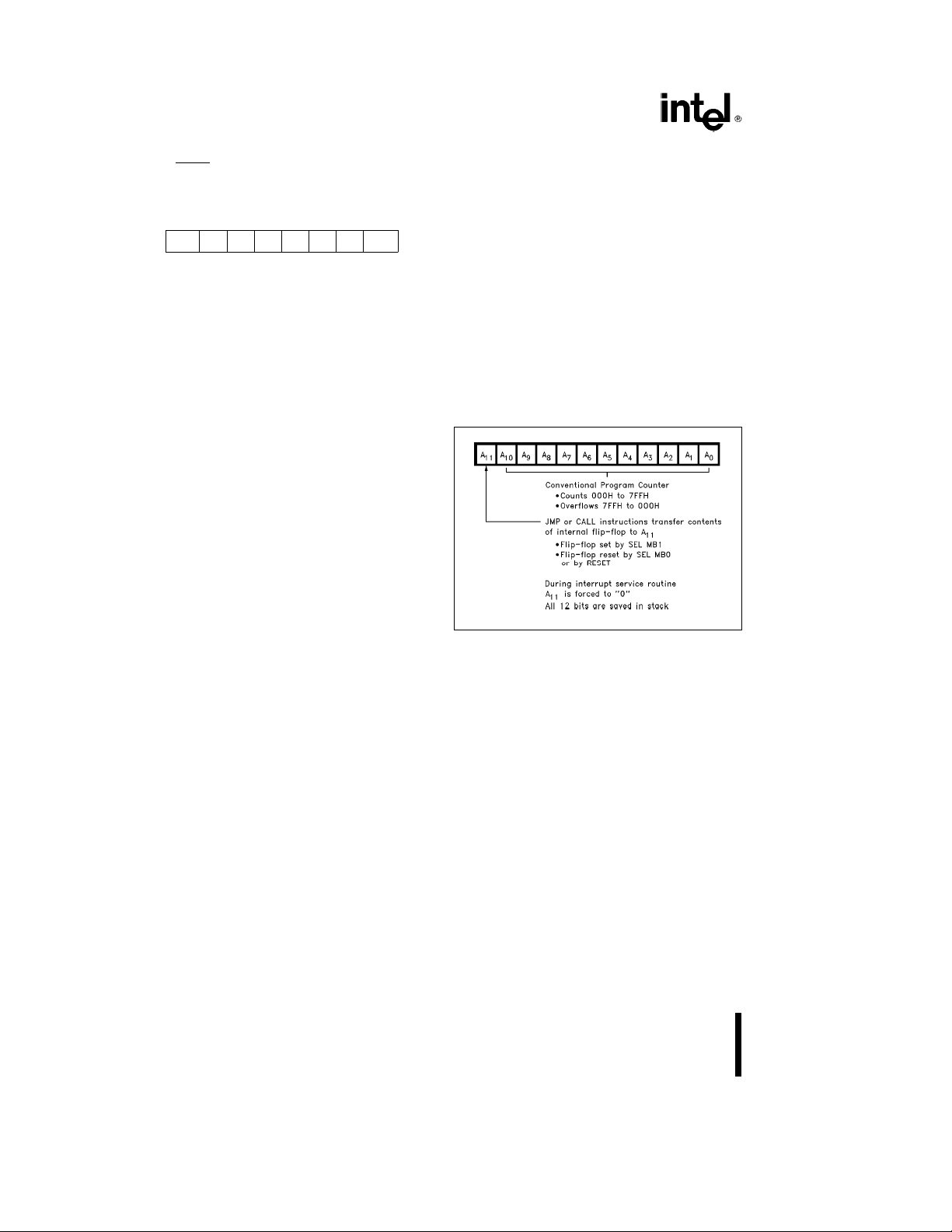
For programs of 2K words or less, the UPI-C42 addresses program memory in the conventional manner. Addresses beyond 2047 can be reached by executing a program memory bank switch instruction
(SEL PMB0, SEL PMB1) followed by a branch instruction (JMP or CALL). The bank switch feature
extends the range of branch instructions beyond
their normal 2K range and at the same time prevents
the user from inadvertently crossing the 2K boundary.
PROGRAM MEMORY BANK SWITCH
The switching of 2K program memory banks is accomplished by directly setting or resetting the most
significant bit of the program counter (bit 11); see
Figure 5. Bit 11 is not altered by normal incrementing of the program counter, but is loaded with the
contents of a special flip-flop each time a JMP or
CALL instruction is executed. This special flip-flop is
set by executing an SEL PMB1 instruction and reset
by SEL PMB0. Therefore, the SEL PMB instruction
may be executed at any time prior to the actual bank
switch which occurs during the next branch instruction encountered. Since all twelve bits of the program counter, including bit 11, are stored in the
stack, when a Call is executed, the user may jump to
subroutines across the 2K boundary and the proper
PC will be restored upon return. However, the bank
switch flip-flop will not be altered on return.
290414– 30
Figure 5. Program Counter
INTERRUPT ROUTINES
Interrupts always vector the program counter to location 3 or 7 in the first 2K bank, and bit 11 of the
program counter is held at ‘‘0’’ during the interrupt
service routine. The end of the service routine is signaled by the execution of an RETR instruction. Interrupt service routines should therefore be contained
entirely in the lower 2K words of program memory.
The execution of a SEL PMB0 or SEL PMB1 instruction within an interrupt routine is not recommended
since it will not alter PC11 while in the routine, but
will change the internal flip-flop.
Hardware A20 Gate Support
This feature has been provided to enhance the performance of the UPI-C42 when being used in a keyboard controller application. The UPI-C42 design
has included on chip logic to support a hardware
GATEA20 feature which eliminates the need to provide firmware to process A20 command sequences,
6

UPI-C42/UPI-L42
thereby providing additional user programmable
memory space. This feature is enabled by the
A20EN instruction and remains enabled until the device is reset. It is important to note that the execution of the A20EN instruction redefines Port 2, bit 1
as a pure output pin with read only characteristics.
The state of this pin can be modified only through a
valid ‘‘D1’’ command sequence (see Table 1). Once
enabled, the A20 logic will process a ‘‘D1’’ command sequence (write to output port) by setting/resetting the A20 bit on port 2, bit 1 (P2.1) without
requiring service from the internal CPU. The host
can directly control the status of the A20 bit. At no
time during this host interface transaction will the
IBF flag in the status register be activated. Table 1
gives several possible GATEA20 command/data sequences and UPI-C42 responses.
Table 1. D1 Command Sequences
A0 R/W DB Pins IBF A20 Comments
1 W D1h 0 n
0 W DFh 0 1 Only DB1 Is Processed
1 W FFH
1 W D1h 0 n Clear A20 Sequence
0 W DDh 0 0
1 W FFh 0 n
1 W D1h 0 n Double Trigger Set
1 W D1h 0 n Sequence
0 W DFh 0 1
1 W FFh 0 n
1 W D1h 0 n Invalid Sequence
1 W XXh
0 W DDh 1 n of A20 Bit
(2)
(3)
(1)
Set A20 Sequence
0n
1 n No Change in State
SUSPEND
The execution of the suspend instruction (82h or
E2h) causes the UPI-C42 to enter the suspend
mode. In this mode of operation the oscillator is not
running and the internal CPU operation is stopped.
The UPI-C42 consumes
mode. This mode can only be exited by RESET.
CPU operation will begin from PC
s
40 mA in the suspend
e
000h when the
UPI-C42 exits from the suspend power down mode.
Suspend Mode Summary
Oscillator Not Running
#
CPU Operation Stopped
#
Ports Tristated with Weak (E2–10 mA) Pull-Up
#
Micropower Mode (I
#
This mode is exited by RESET
#
CC
s
40 mA)
NOTES:
1. Indicates that P2.1 remains at the previous logic level.
2. Only FFh commands in a valid A20 sequence have no
effect on IBF. An FFh issued at any other time will activate
IBF.
3. Any command except D1.
The above sequences assume that the GATEA20
logic has been enabled via the A20EN instruction.
As noted, only the value on DB 1 (data bus, bit 1) is
processed. This bit will be directly passed through to
P2.1 (port 2, bit 1).
7

UPI-C42/UPI-L42
Table 2 covers all suspend mode pin states. In addition to the suspend power down mode, the UPI-C42
will also support the NMOS power down mode as
outlined in Chapter 4 of the UPI-42AH users manual.
Table 2. Suspend Mode Pin States
Pins Suspend
Ports 1 and 2
Outputs Tristate
Inputs Weak Pull-Up
Disabled
(1)
DBB
Outputs Normal
Inputs Normal
System Control Disabled
Ý
(RD
,WRÝ,
Ý
, A0)
CS
Ý
Reset
Enabled
Crystal Osc. Disabled
(XTAL1, XTAL2)
Test 0, Test 1 Disabled
Prog High
Sync High
EA Disabled,
No Pull-Up
Ý
SS
Disabled,
Weak Pull-Up
I
CC
NOTES:
1. DBB outputs are Tristate unless CS
tive. DBB inputs are disabled unless CS
active.
2. A ‘‘disabled’’ input will not cause current to be drawn
regardless of input level (within the supply range).
3. Weak pull-ups have current capability of typically 5 mA.
k
40 mA
Ý
and RDÝare ac-
Ý
and WRÝare
NEW UPI-C42 INSTRUCTIONS
The UPI-C42 will support several new instructions to
allow for the use of new C42 features. These instructions are not necessary to the user who does
not wish to take advantage of any new C42 functionality. The C42 will be completely compatible with all
current NMOS code/applications. In order to use
new features, however, some code modifications will
be necessary. All new instructions can easily be inserted into existing code by use of the ASM-48 macro facility as shown in the following example:
Macname MACRO
DB 63H
ENDM
New Instructions
The following is a list of additions to the UPI-42 instruction set. These instructions apply only to the
UPI-C42. These instructions must be added to existing code in order to use any new functionality.
SEL PMB0 Select Program Memory Bank 0
OPCODE 0110 0011 (63h)
PC Bit 11 is set to zero on next JMP or CALL instruction. All references to program memory fall within
the range of 0– 2047 (0 – 7FFh).
SEL PMB1 Select Program Memory Bank 1
OPCODE 0111 0011 (73h)
PC Bit 11 is set to one on next JMP or CALL instruction. All references to program memory fall within
the range of 2048– 4095 (800h – FFFh).
ENA20 Enables Auto A20 hardware
OPCODE 0011 0011 (33h)
Enables on chip logic to support Hardware A20 Gate
feature. Will remain enabled until device is reset.
8
 Loading...