*Other brands and names are the property of their respective owners.
Information in this document is provided in connection with Intel products. Intel assumes no liability whatsoever, including infringement of any patent or
copyright, for sale and use of Intel products except as provided in Intel’s Terms and Conditions of Sale for such products. Intel retains the right to make
changes to these specifications at any time, without notice. Microcomputer Products may have minor variations to this specification known as errata.
November 1995COPYRIGHT©INTEL CORPORATION, 1996 Order Number: 281732-001
82595FX
ISA BUS HIGH INTEGRATION
ETHERNET CONTROLLER
Y
Optimal Integration for Lowest Cost
Solution
Ð Glueless 8-Bit/16-Bit ISA Bus
Interface
Ð Provides Fully 802.3 Compliant AUI
and TPE Serial Interface
Ð Local SRAM Support up to 64 Kbytes
Ð Integrated ISA Bus Data
Transceivers
Ð FLASH/EPROM Boot Support up to
1 Mbyte for Diskless Workstations
Ð Hardware and Software Portable
between Motherboard and Adapter
Card Solutions
Y
High Performance Networking
Functions
Ð Advanced Concurrent Processing of
Receive and Transmit Functions
Ð 16-Bit/32-Bit IO Accesses to Local
SRAM with Zero Added Wait-States
Ð Ring Buffer Structure for Continuous
Frame Reception and Transmit
Chaining
Ð Automatic Retransmission on
Collision
Ð Automatically Corrects TPE Polarity
Switching Problems
Ð Auto Negotiation/Manual Full Duplex
Support
Y
Low Power CHMOS IV Technology
Y
Ease of Use
Ð Auto-Negotiation of Full Duplex
Functionality
Ð Fully Compatible with ISA Plug and
Play Specification
Ð EEPROM Interface to Support
Jumperless Designs
Ð Software Structures Optimized to
Reduce Processing Steps
Ð Automatically Maps into Unused PC
IO Locations to Help Eliminate LAN
Setup Problems
Ð All Software Structures Contained in
One 16-Byte IO Space
Ð JTAG Port for Reduced Board
Testing Times
Ð Automatic or Manual Switching
between TPE and AUI Ports
Ð Supports Eight IRQs
Y
Power Management
Ð Advanced Power Management
Support by Power Down and Sleep
Mode
Ð Both SL Compatible SMOUT Input
and Non-SL Software Parameter for
Power Down Mode
Y
160-Lead QFP Package Provides
Smallest Available Form Factor
Y
100% Backwards Software Compatible
to 82595TX
281732– 1
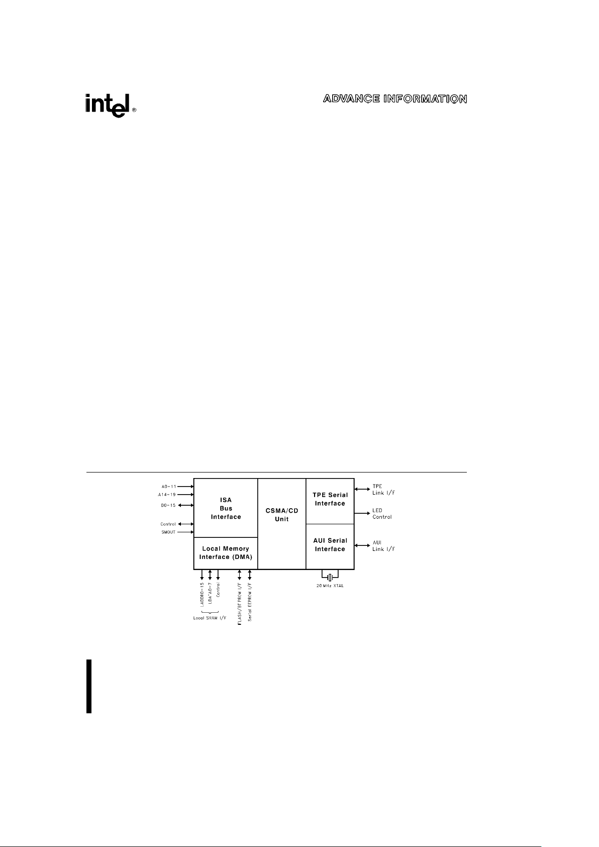
Figure 1. 82595FX Block Diagram

82595FX
ISA Bus High Integration ETHERNET Controller
CONTENTS PAGE
1.0 INTRODUCTION ААААААААААААААААААААААА 5
1.1 82595FX Overview АААААААААААААААААА 5
1.2 Power Management ААААААААААААААААА 5
1.3 Auto-Negotiation АААААААААААААААААААА 5
1.4 Compliance to Industry
Standards
АААААААААААААААААААААААААААА 6
1.4.1 Bus InterfaceÐISA IEEE
P996 АААААААААААААААААААААААААААААА 6
1.4.2 ETHERNET/Twisted Pair
Ethernet InterfaceÐIEEE 802.3
Specification
ААААААААААААААААААААААА 6
2.0 82595FX PIN DEFINITIONS ААААААААААА 6
2.1 ISA Bus Interface АААААААААААААААААААА 6
2.2 Local Memory Interface АААААААААААААА 8
2.3 Miscellaneous Control ААААААААААААААА 9
2.4 JTAG Control АААААААААААААААААААААААА 9
2.5 Serial Interface АААААААААААААААААААААА 9
2.6 Serial Interface LEDs ААААААААААААААА 10
2.7 Power and Ground ААААААААААААААААА 11
2.8 Reserved Pins АААААААААААААААААААААА 11
2.9 82595FX Pin Summary ААААААААААААА 12
3.0 82595FX INTERNAL
ARCHITECTURE OVERVIEW АААААААААА 13
3.1 System Interface Overview ААААААААА 13
3.1.1 Concurrent Processing
Functionality АААААААААААААААААААААА 13
3.2 Local Memory Interface АААААААААААА 13
3.3 CSMA/CD Unit ААААААААААААААААААААА 14
3.4 Serial Interface ААААААААААААААААААААА 14
4.0 ACCESSING THE 82595FX ААААААААААА 14
4.1 82595FX Register Map ААААААААААААА 14
4.1.1 IO Bank 0 ААААААААААААААААААААА 15
4.1.2 IO Bank 1 ААААААААААААААААААААА 16
4.1.3 IO Bank 2 ААААААААААААААААААААА 17
4.2 Writing to the 82595FX ААААААААААААА 17
4.3 Reading from the 82595FX ААААААААА 18
CONTENTS PAGE
4.4 Local SRAM Accesses
ААААААААААААА 18
4.4.1 Writing to Local Memory ААААААА 18
4.4.2 Reading from Local
Memory АААААААААААААААААААААААААА 18
4.5 Serial EEPROM Interface ААААААААААА 19
4.6 Boot EPROM/FLASH Interface ААААА 20
5.0 COMMAND AND STATUS
INTERFACE АААААААААААААААААААААААААААА 20
5.1 Command OP Code Field ААААААААААА 20
5.2 ABORT (Bit 5) АААААААААААААААААААААА 20
5.3 Pointer Field (Bits 6 and 7) АААААААААА 20
5.4 82595FX Status Interface ААААААААААА 22
6.0 INITIALIZATION АААААААААААААААААААААА 22
7.0 FRAME TRANSMISSION ААААААААААААА 23
7.1 82595FX XMT Block Memory
Format АААААААААААААААААААААААААААААА 23
7.2 XMT Chaining АААААААААААААААААААААА 25
7.3 Automatic Retransmission on
Collision
ААААААААААААААААААААААААААААА 28
8.0 FRAME RECEPTION ААААААААААААААААА 28
8.1 82595FX RCV Memory
Structure АААААААААААААААААААААААААААА 28
8.2 RCV Ring Buffer Operation ААААААААА 31
9.0 SERIAL INTERFACE ААААААААААААААААА 32
10.0 APPLICATION NOTES АААААААААААААА 33
10.1 Bus Interface АААААААААААААААААААААА 33
10.2 Local Memory Interface ААААААААААА 33
10.3 EEPROM Interface (ISA Only) ААААА 33
10.4 Serial Interface АААААААААААААААААААА 33
10.4.1 AUI Circuit ААААААААААААААААААА 33
10.4.2 TPE Circuit ААААААААААААААААААА 34
10.4.3 LED Circuit ААААААААААААААААААА 34
2

CONTENTS PAGE
10.5 Layout Guidelines
ААААААААААААААААА 34
10.5.1 General АААААААААААААААААААААА 34
10.5.2 Crystal ААААААААААААААААААААААА 34
10.5.3 82595FX Analog Differential
Signals ААААААААААААААААААААААААААА 34
10.5.4 Decoupling
Considerations АААААААААААААААААААА 34
11.0 ELECTRICAL SPECIFICATIONS
AND TIMINGS АААААААААААААААААААААААААА 35
11.1 Absolute Maximum Ratings АААААААА 35
11.1.1 Package Thermal
Specifications ААААААААААААААААААААА 36
CONTENTS PAGE
11.2 AC Timing Characteristics
ААААААААА 36
11.3 AC Measurement Conditions АААААА 36
11.4 ISA Interface Timing ААААААААААААААА 37
11.6 Local Memory Timings АААААААААААА 41
11.6.1 SRAM Timings ААААААААААААААА 41
11.6.2 FLASH/EPROM Timings ААААА 43
11.7 Interrupt Timing ААААААААААААААААААА 45
11.8 RESET and SMOUT Timing ААААААА 46
11.9 JTAG Timing АААААААААААААААААААААА 47
11.10 Serial Timings ААААААААААААААААААА 48
3
82595FX
281732– 2
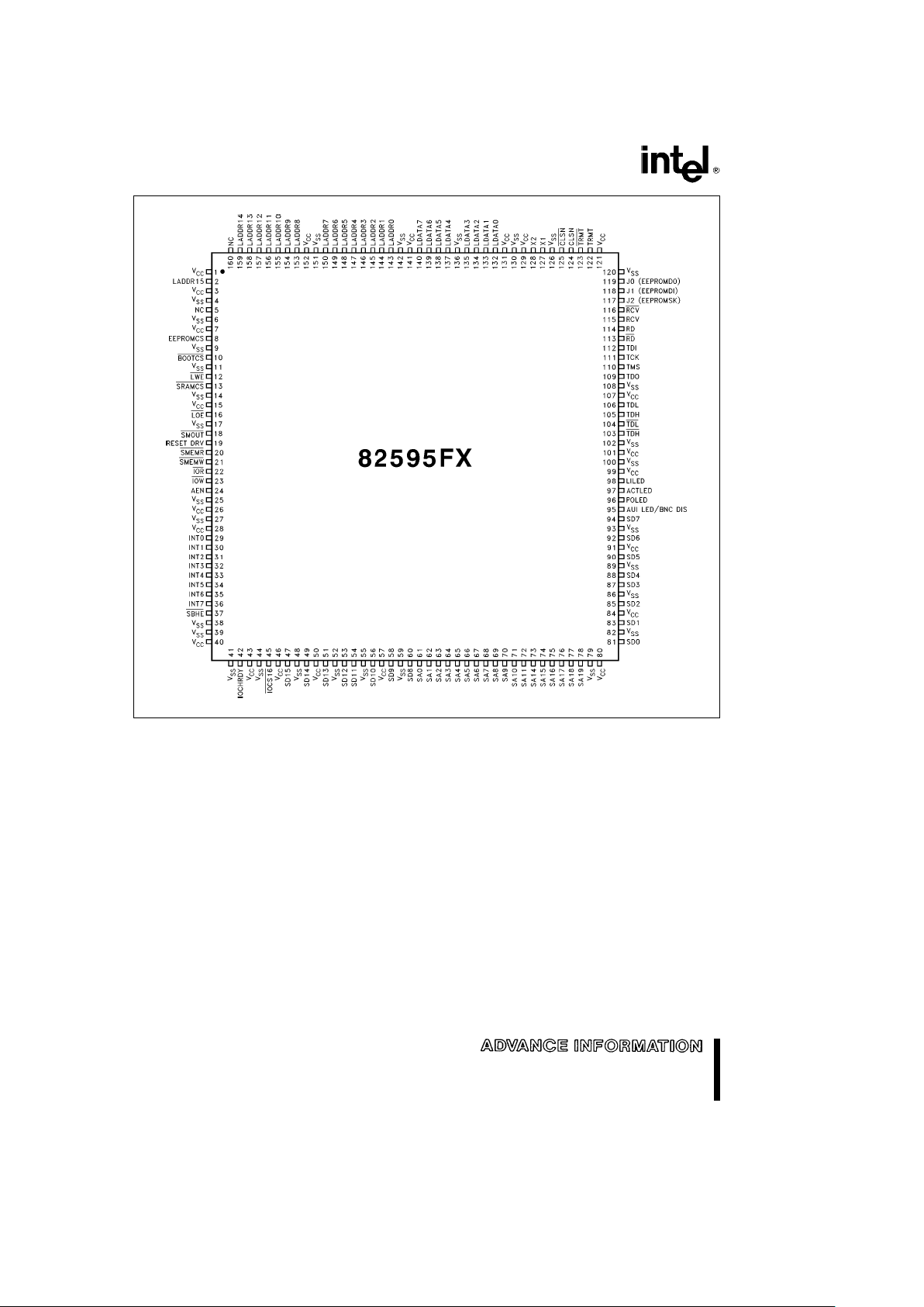
Figure 2. 82595FX Pinout
4

82595FX
1.0 INTRODUCTION
1.1 82595FX Overview
The 82595FX is a highly integrated, high performance LAN controller which provides a cost effective
LAN solution for ISA compatible Personal Computer
(PC) motherboards (both desktop and portable), and
add-on ISA adapter boards. The 82595FX integrates
all of the major functions of a buffered LAN solution
into one chip with the exception of the local buffer
memory, which is implemented by adding one SRAM
component to the LAN solution. The 82595FX’s
Concurrent Processing feature significantly enhances throughput performance. Both system bus and
serial link activities occur concurrently, allowing the
82595FX to maximize network bandwidth by minimizing delays associated with transmit or receiving
frames. The 82595FX’s bus interface is a glueless
attachment to an ISA bus. Its serial interface provides a Twisted Pair Ethernet (TPE) and an Attachment Unit Interface (AUI) connection. By integrating
the majority of the LAN solution functions into one
cost effective component, production cost saving
can be achieved as well as significantly decreasing
the design time for a solution. This level of integration also allows an 82595FX solution to be ported
between different applications (PC motherboards,
and adapters, while maintaining a compatible hardware and software base.
The 82595FX’s software interface is optimized to reduce the number of processing steps that are required to interface to the 82595FX solution. The
82595FX’s initialization and control registers are directly addressable within one 16-byte IO address
block. The 82595FX can automatically resolve any
conflicts to an IO block by moving its IO offset to an
unused location in the case that a conflict occurs.
The 82595FX’s local memory is arranged in a simple
ring buffer structure for efficient transfer of transmit
and receive packets. The local memory, up to
64 Kbytes of SRAM, resides as either a 16-bit or 32bit IO port in the host systems IO map programmable through configuration. The 82595FX provides direct control over the local SRAM. The 82595FX performs a prefetch to the SRAM memory allowing CPU
IO cycles to this data with no added wait-states. The
82595FX also provides an interface to up to 1 Mbyte
of FLASH or EPROM memory. An interface to an
EEPROM, which holds solution configuration values
and can also contain the Node ID, allows for the
implementation of a ‘‘jumperless’’ design. In addition, the 82595FX contains full hardware support for
the implementation of the ISA Plug N’ Play specification. Plug N’ Play eliminates jumpers and complicated setup utilities by allowing peripheral functions to
be added to a PC automatically (such as adapter
cards) without the need to individually configure
each parameter (e.g. Interrupt, IO Address, etc).
This allows for configuration ease-of-use, which results in minimal time associated with installation.
The 82595FX’s packaging and power management
features are designed to consume minimal board
real estate and system power. This is required for
applications such as portable PC motherboard designs which require a solution with very low real estate and power consumption. The 82595FX package
is a 160-lead PQFP (Plastic Quad Flat Pack). Its dimensions are 28 mm by 28 mm, and 3.5 mm in
height. The 82595FX contains two power down
modes; an SL compatible power down mode which
utilizes the SL SMOUT input, and a POWER DOWN
command for non-SL systems.
1.2 Power Management
Power management and low power consumption are
two items that will allow any design using the
82595FX to be suitable for green PC use. Low power operation is initiated when software issues a
SLEEP command to the device. After a short wait, it
will shut off the system clock, some parts of the
Backoff Randomizer, several input buffers and the
two LED drivers. The 82595FX will subsequently
wake up from sleep mode when software initiates an
ISA cycle in the application, as well as when it receives a frame addressed to it. The total power consumption when in sleep mode can be as low as approximately 175 mW. Normal idle power consumption is 300 mW.
The software POWER DOWN command, along with
its companion hardware implementationÐthe
SMOUT I/O pin, provide additional power management capabilities. This feature allows the 82595FX
to be powered down, and then at some time in the
future be selectively reset without having lost the
current configuration. See the 82595FX User’s
Guide for further details on these features.
1.3 Auto-Negotiation
Auto-negotiation functionality is a method of automatically determining the highest common operating
mode (i.e., 10BaseT half duplex, 10BaseT full duplex, etc.) between two network devices. Using this
functionality, two stations, each having a varying
number of different operating modes, negotiate the
highest possible common operating mode between
them. During the power up sequence, the auto-negotiation functionality will automatically establish a
link with which it can take advantage of any auto-negotiation-capable device it is connected to. An autonegotiation capable hub can detect and automatically configure its ports to take maximum advantage of
5
82595FX
common modes of operation without any user intervention or prior knowledge by connected stations.
See the 82595FX User’s Guide for details on this
function.
For further information on these enhancements
and a description of all the differences between
the 82595TX and 82595FX, please consult the
82595FX User’s Manual, available through your
local sales representative.
1.4 Compliance to Industry Standards
The 82595FX has two interfaces; the host system
interface, which is an ISA bus interface, and the serial, or network interface. This interface has been
standardized by the IEEE.
1.4.1 BUS INTERFACEÐ
ISA IEEE P996
The 82595FX implements the full ISA bus interface.
It is compatible with the IEEE spec P996.
1.4.2 ETHERNET/TWISTED PAIR ETHERNET
INTERFACEÐIEEE 802.3 SPECIFICATION
The 82595FX’s serial interface provides either an
AUI port interface or a Twisted Pair Ethernet (TPE)
interface. The AUI port can be connected to an
Ethernet Transceiver cable drop, providing a fully
compliant IEEE 802.3 AUI interface. The TPE port
provides a fully compliant IEEE 10BASE-T interface.
The 82595FX can automatically switch to whichever
port (TPE or AUI) is active.
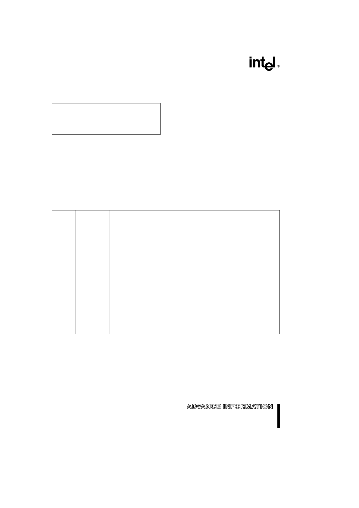
2.0 82595FX PIN DEFINITIONS
2.1 ISA Bus Interface
Symbol
Pin
Type Name and Function
No.
SA0 61 I ADDRESS BUS: These pins provide address decoding for up to 1 Kbyte of
address. These pins also provide 4 Kbytes of IO addressing to support the
SA1 62
Plug N’ Play Standard.
SA2 63
SA3 64
SA4 65
SA5 66
SA6 67
SA7 68
SA8 69
SA9 70
SA10 71
SA11 72
SA14 73 I ADDRESS BUS: These pins provide address decoding between the 16 Kbyte
and 1 Mbyte memory space. This allows for decoding of a Boot EPROM or a
SA15 74
FLASH in 16K increments.
SA16 75
SA17 76
SA18 77
SA19 78
6
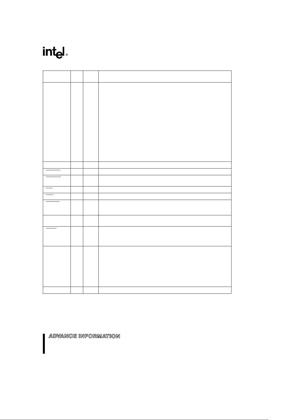
82595FX
2.1 ISA Bus Interface (Continued)
Symbol
Pin
Type Name and Function
No.
SD0 81 I/O DATA BUS: This is the data interface between the 82595FX and the host
system. This data is buffered by one (8-bit design) or two (16-bit design)
SD1 83
internal transceivers.
SD2 85
SD3 87
SD4 88
SD5 90
SD6 92
SD7 94
SD8 60
SD9 58
SD10 56
SD11 54
SD12 53
SD13 51
SD14 49
SD15 47
AEN 24 I ADDRESS ENABLE: Active high signal indicates a DMA cycle is active.
SMEMR 20 I MEMORY READ for system memory accesses below 1 Mbyte. Active low.
SMEMW 21 I MEMORY WRITE for system memory accesses below 1 Mbyte. Active
low.
IOR 22 I IO READ: Active low.
IOW 23 I IO WRITE: Active low.
IOCS16 45 O IO CHIP SELECT 16: Active low, open drain output which indicates that
an IO cycle access to the 82595FX solution is 16-bit wide. Driven for IO
cycles to the local memory or to the 82595FX.
IOCHRDY 42 O IO CHANNEL READY: Active high, open drain output. When driven low, it
extends host cycles to the 82595FX solution.
SBHE 37 I SYSTEM BUS HIGH ENABLE: Active low input indicates a data transfer
on the high-byte (D8 – D15) of the system bus (a 16-bit transfer). This pin
also determines if the 82595FX is operating in an 8- or 16-bit system upon
initialization.
INT0 29 O 82595FX INTERRUPT 0 – 7: One of these 8 pins is selected to be active
one at a time (the other seven are in Hi-Z state) by configuration. These
INT1 30
active high outputs serve as interrupts to the host system.
INT2 31
INT3 32
INT4 33
INT5 34
INT6 35
INT7 36
RESET DRV 19 I RESET DRIVE: Active high reset signal.
7
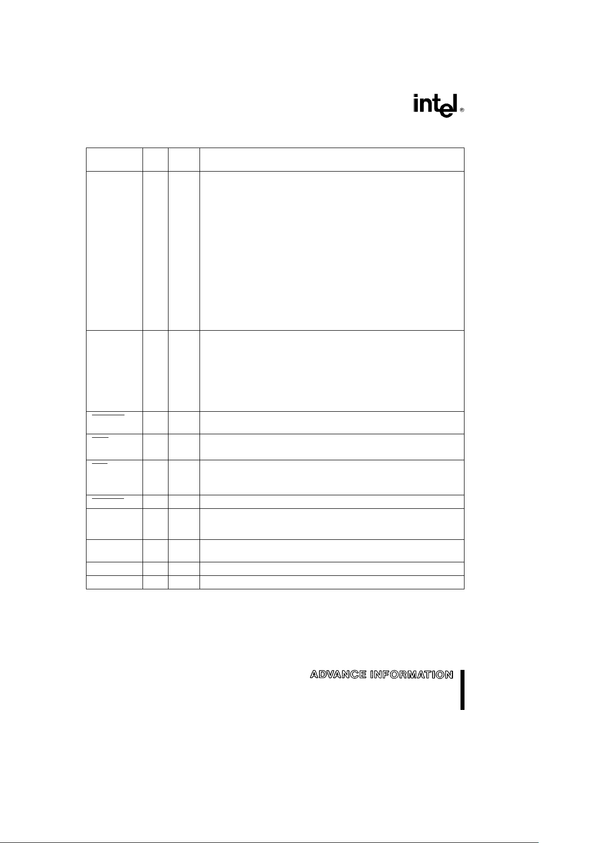
82595FX
2.2 Local Memory Interface
Symbol
Pin
Type Name and Function
No.
LADDR0 143 O LOCAL MEMORY ADDRESS (LADDR0 – LADDR15): These outputs
contain the multiplexed address for the local SRAM.
LADDR1 144
LADDR2 145
FLASH ADDRESS 14 – 17 (LADDR0 – LADDR5): These pins control the
LADDR3 146
FLASH addressing from 16K to 1M to allow paging of the FLASH in 16K
LADDR4 147 spaces. These addresses are under direct control of the FLASH PAGING
configuration register.
LADDR5 148
LADDR6 149
LADDR7 150
LADDR8 153
LADDR9 154
LADDR10 155
LADDR11 156
LADDR12 157
LADDR13 158
LADDR14 159
LADDR15 2
LDATA0 132 I/O LOCAL MEMORY DATA BUS (LDATA0– LDATA7): The eight I/O
signals, comprising the local data bus, are used to read or write data to or
LDATA1 133
from the 8-bit wide SRAM.
LDATA2 134
LDATA3 135
FLASH MEMORY DATA BUS (LDATA0–LDATA7): These signals also
LDATA4 137 provide eight bits of data for accesses to an 8-bit FLASH/EPROM if these
components are used.
LDATA5 138
LDATA6 139
LDATA7 140
SRAMCS 13 O SRAM CHIP SELECT: This active low output is the chip select to the
SRAM.
LWE 12 O This active low output is the Write Enable to the SRAM.
This pin also provides the active low Write Enable to the FLASH.
LOE 16 O This active low output is the Output Enable to the SRAM.
This pin also provides the active low Output Enable control to the
FLASH.
BOOTCS 10 O BOOT EPROM/FLASH CHIP SELECT: Active low output.
EEPROMCS 8 I/O EEPROM CS: Active high signal. If no EEPROM is connected, this pin
should be connected to V
CC
. In this case it will function as an input to the
82595FX to indicate no EEPROM is connected.
EEPROMSK 117 O EEPROM SHIFT CLOCK: This output is used to shift data into and out of
the serial EEPROM.
EEPROMDO 119 O EEPROM DATA OUT
EEPROMDI 118 O EEPROM DATA IN
8
82595FX
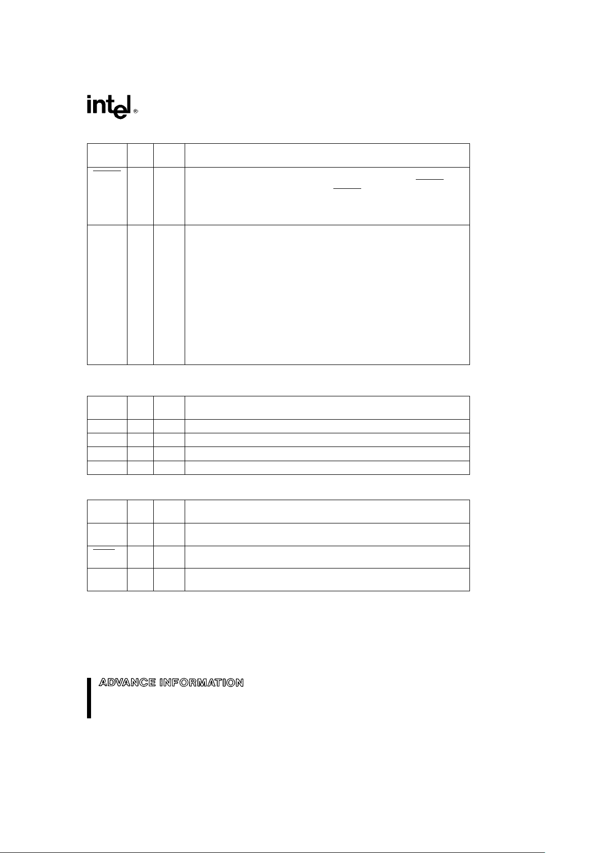
2.4 Miscellaneous Control
Symbol
Pin
Type Name and Function
No.
SMOUT 18 I/O This active LOW signal, when asserted, places the 82595FX into a Power
Down mode. The 82595FX will remain in power down mode until SMOUT
is
unasserted. If this line is unconnected to SMOUT
from the system bus, it can
be used as an active low output which, when a POWER DOWN command is
issued to the 82595FX, can be used to power down other external
components (this output function is enabled by configuration).
J0 119 I JUMPER: Input for selecting between 7 ISA IO spaces. These pins should be
connected to either V
CC
or GND or the EEPROM. The 82595FX reads the
J1 118 I
Jumper block during its initialization sequence.
J2 117 I
J0 J1 J2 IO Address
Connected to EEPROM Configuration contained in EEPROM
GND GND GND I/O Window Disabled
V
CC
GND GND 2A0h
GND V
CC
GND 280h
V
CC
V
CC
GND 340h
GND GND V
CC
300h
V
CC
GND V
CC
360h
GND V
CC
V
CC
350h
V
CC
V
CC
V
CC
330h
2.4 JTAG Control
Symbol
Pin
Type Name and Function
No.
TDO 109 O JTAG TEST DATA OUT
TMS 110 I JTAG TEST MODE SELECT
TCK 111 I JTAG TEST CLOCK
TDI 112 I JTAG TEST DATA IN
2.5 Serial Interface
Symbol
Pin
Type Name and Function
No.
TRMT 122 O Positive side of the differential output driver pair that drives 10 Mb/s
Manchester Encoded data on the TRMT pair of the AUI cable (Data Out A).
TRMT 123 O Negative side of the differential output driver pair that drives 10 Mb/s
Manchester Encoded data on the TRMT pair of the AUI cable (Data Out B).
RCV 115 I The positive input to a differential amplifier connected to the RCV pair of the
AUI cable (Data In A). It is driven with 10 Mb/s Manchester Encoded data.
9
82595FX
2.5 Serial Interface (Continued)
Symbol
Pin
Type Name and Function
No.
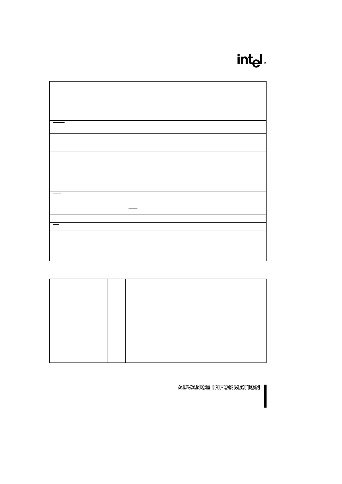
RCV 116 I The negative input to a differential amplifier connected to the RCV pair of the
AUI cable (Data In B). It is driven with 10 Mb/s Manchester Encoded data.
CLSN 124 I The positive input to a differential amplifier connected to the CLSN pair of the
AUI cable (Collision In A).
CLSN 125 I The negative input to a differential amplifier connected to the CLSN pair of the
AUI cable (Collision In B).
TDH 105 O TRANSMIT DATA HIGH: Active high Manchester Encoded data to be
transmitted onto the twisted pair. This signal is used in conjunction with TDL,
TDH
, and TDL to generate the pre-conditioned twisted pair output waveform.
TDL 106 O TRANSMIT DATA LOW: Twisted Pair Output Driver. Active high Manchester
Encoded data with embedded pre-distortion information to be transmitted onto
the twisted pair. This signal is used in conjunction with TDH, TDH
, and TDL
to
generate the pre-conditioned twisted pair output waveform.
TDH 103 O TRANSMIT DATA HIGH INVERT: Active low Manchester Encoded data to be
transmitted onto the twisted pair. This signal is used in conjunction with TDL,
TDH, and TDL
to generate the pre-conditioned twisted pair output waveform.
TDL 104 O TRANSMIT DATA LOW INVERT: Twisted Pair Output Driver. Active low
Manchester Encoded data with embedded pre-distortion information to be
transmitted onto the twisted pair. This signal is used in conjunction with TDL,
TDH, and TDH
to generate the pre-conditioned twisted pair output waveform.
RD 114 I Active high Manchester Encoded data received from the twisted pair.
RD 113 I Active low Manchester Encoded data received from the twisted pair.
X1 127 I 20 MHz CRYSTAL INPUT: This pin can be driven with an external MOS level
clock when X2 is left floating. This input provides the timing for all of the
82595FX functional blocks.
X2 128 O 20 MHz CRYSTAL OUTPUT: If X1 is driven with an external MOS level clock,
X2 should be left floating.
2.6 Serial Interface LEDs
Symbol
Pin
Type Name and Function
No.
AUI LED/BNC DIS 95 O AUI LED INDICATOR: This output, when the 82595FX is used as a
TPE/AUI solution, will turn on an LED when the 82595FX is actively
interfaced to its AUI serial port. When the 82595FX is used as a
BNC/AUI solution, this output becomes the BNC DIS output, which
can be used to power down the BNC Transceiver section (the
Transceiver and the DC to DC Converter) of the solution when the
BNC port is unconnected.
LILED 98 O LINK INTEGRITY LED: Normally on (low) ouput which indicates a
good link integrity status when the 82595FX is connected to an
active TPE port. This output will remain on when the Link Integrity
function has been disabled. It turns off (driven high) when Link
Integrity fails, or when the 82595FX is actively interfaced to an AUI
port. The minimum off time is 100 ms.
10
82595FX
2.6 Serial Interface LEDs (Continued)
Symbol
Pin
Type Name and Function
No.
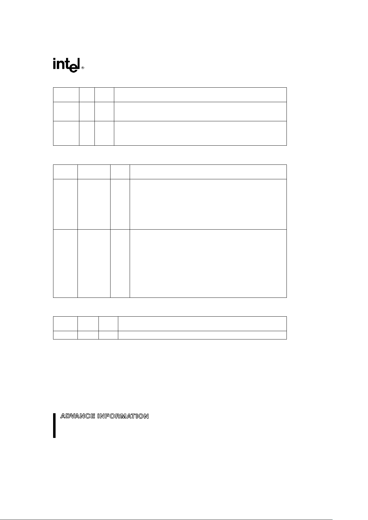
ACTLED 97 O LINK ACTIVITY LED: Normally off (high) output turns on to indicate activity
for transmission, reception, or collision. Flashes at a rate dependent on the
level of activity on the link.
POLED 96 O POLARITY LED: If the 82595FX detects that the receive TPE wires are
reversed, the POLED will turn on (low) to indicate the fault. POLED remains on
even if automatic polarity correction is enabled, and the 82595FX has
automatically corrected for the reversed wires.
2.7 Power and Ground
Symbol
Pin
Type Name and Function
No.
V
CC
1, 3, 7, 15, I POWER:a5Vg5%.
26, 28, 40,
43, 46, 50,
57, 80, 84,
91, 99, 101,
107, 121,
129, 131,
141, 152
V
SS
4, 6, 9, 11, I GROUND: 0V.
14, 17, 25,
27, 38, 39,
41, 44, 48,
52, 55, 59,
79, 82, 86,
89, 93, 100,
102, 108,
120, 126,
130, 136,
142, 151
2.8 Reserved Pins
Symbol
Pin
Type Name and Function
No.
N/C 5, 160 Reserved. Do not connect.
11
82595FX
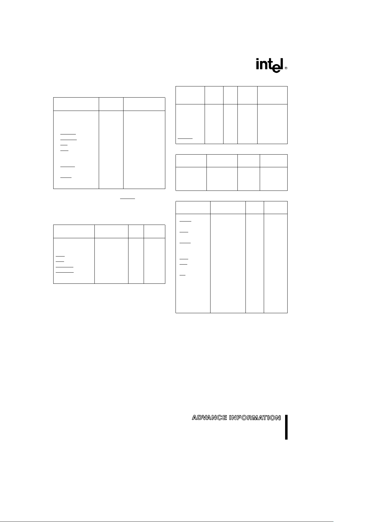
2.9 82595FX Pin Summary
ISA Bus Interface
ISA Pin P-Down
Pin Name Type State
SA0–SA3 (In) Inactive
SA4–SA11 Inactive/Act
(1)
SA14–19 (In) Inactive
SD0–SD15 (I/O) TS TS
SMEMR
(In) Inactive
SMEMW (In) Inactive
IOR
(In) Inactive
IOW
(In) Inactive/Act
(1)
INT0–7 (Out) TS TS
RESET DRV (In) Act
IOCS16
(Out) OD TS
IOCHRDY (Out) OD TS
SBHE
(In) Inactive
AEN (In) Inactive/Act
(1)
NOTE:
1. For hardware powerdown using SMOUT
, these pins will
be inactive. For software powerdown, these pins remain
active.
Local Memory Interface
Pin MUXed Pin
P-Down
Name Name Type
LADDR[5:0](Out) FADDR[14:19]2S TS
LADDR[6:15](Out) 2S TS
LDATA[0:7](I/O) TS TS
LWE
(Out) 2S TS
LOE
(Out) 2S TS
BOOTCS (Out) 2S PU
SRAMCS
(Out) 2S PU
EEPROMCS (I/O) TS PD
Miscellaneous Control
MUXed
Pin P-Down Dual
Pin Name Pin
Type State Pin Name
Name
J0(In) ACT EEPROM2D0
(In)
J1 (I/O) TS TS EEPROM2DI
(Out)
J2 (I/O) TS TS EEPROM2SK
(Out)
SMOUT
(I/O) TS ACT/TS
JTAG Control
Pin Name
MUXed Pin P-Down
Pin Name Type State
TMS (In) In Act
TCK (In) In Act
TDI (In) In Act
TDO (Out) TS
Serial Interface
Pin Name
MUXed Pin P-Down
Pin Name Type State
TRMT (Out) Ana TS
TRMT
(Out) Ana TS
RCV (In) Ana In Act
RCV
(In) Ana In Act
CLSN (In) Ana In Act
CLSN (In) Ana In Act
TDH (Out) Ana TS
TDL (Out) Ana TS
TDH
(Out) Ana TS
TDL
(Out) Ana TS
RD (In) Ana In Act
RD
(In) Ana In Act
X1 (In) In Act
X2 (Out) 2S TS
LILED (Out) 2S TS*
POLED (Out) 2S TS*
ACTLED (Out) 2S TS*
AUILED (Out) BNC DIS (Out) 2S TS*
*Assuming auto-negotiation disabled.
Legend:
TSÐTriState.
ODÐOpen Drain.
2SÐTwo State, will be found in eithera1or0logic level.
AnaÐAnalog pin (all serial interface signals).
ActÐInput buffer is active during Power Down.
In ActÐInput buffer is inactive during Power Down.
PUÐOutput in inactive state with weak internal Pull-up during Power Down.
PDÐOutput in inactive state with weak internal Pull-down during Power Down.
DualÐDual function pin.
12

82595FX
3.0 82595FX INTERNAL
ARCHITECTURE OVERVIEW
Figure 1 shows a high level block diagram of the
82595FX. The 82595FX is divided into four main
subsections; a system interface, a local memory
sub-system interface, a CSMA/CD unit, and a serial
interface.
3.1 System Interface Overview
The 82595FX’s system interface subsection includes a glueless ISA bus interface, and the
82595FX’s IO registers (including the 82595FX’s
command, status, and Data In/Out registers). The
system interface block also interfaces with the
82595FX’s local memory interface subsystem and
CSMA/CD subsystem.
The bus interface logic provides the control, address, and data interface to an ISA compatible bus.
The 82595FX decodes up to 1M of total memory
address space. Address decoding within 16K block
increments (A14–A19) are used for Flash or Boot
EPROM. IO accesses are decoded throughout the 1
Kbyte PC IO address range (A10 and A11 provide up
to 4K of IO addressing and are used for Plug N’
Play). The 82595FX data bus interface provides either an 8- or 16-bit interface to the host system’s
data bus. The control interface provides complete
handshaking interface with the system bus to enable
transfer of data between the 82595FX solution and
the host system.
The 82595FX’s IO registers provide 3 banks of directly addressable registers which are used as the
control and data interface to the 82595FX. There
are 16 IO registers per bank, with only one bank
enabled at a time. This allows the complete
82595FX software interface to be contained in one
16-byte IO space. The base address of this IO space
is selectable via either software (which can be
stored in a serial EEPROM), or by strapping the
82595FX IO Jumper block (J0 –J2). The 82595FX
can also detect conflicts to its base IO space, and
automatically resolve these conflicts either by allowing the selection of one Plug N’ Play card from multiple cards (using Plug N’ Play software), or by mapping itself into an un-used IO space (Automatic IO
Resolution). Included in the 82595FX IO registers
are the Command Register, the Status Register, and
the Local Memory IO Port register, which provides
the data interface to the local SRAM buffer contained in an 82595FX solution. Functions such as IO
window mapping, Interrupt enable, RCV and XMT
buffer initialization, etc. are also configured and controlled through the IO registers.
3.1.1 CONCURRENT PROCESSING
FUNCTIONALITY
The 82595FX’s Concurrent Processing feature significantly enchances data throughput performance
by performing both system bus and serial link activities concurrently. Transmission of a frame is started
by the 82595FX before that frame is completely copied into local memory. During reception, a frame is
processed by the host CPU before that frame is entirely copied to local memory. Transmit Concurrent
Processing feature is enabled by writing to BANK 2,
Register 1, Bit 0. A 1 written to this bit enables this
functionality, a 0 (default) disables it. To enable Receive Concurrent Processing, BANK 1, Register 7
must be programmed to value other than 00h (00h
disables RCV Concurrent Processing, and is default). (See Section 4.1 for the format of IO BANK 1
and 2.) Improvements in concurrent processing
functionality have allowed the 82595FX to include
enhancements to the throughput efficiency of the
82595TX. For details, refer to the 82595FX User’s
Guide. Concurrent Processing is not recommended
for 8-bit interfaces. For more information on Transmit and Receive Concurrent Processing, refer to
Section 7.0 and Section 8.0.
3.2 Local Memory Interface
The 82595FX’s local memory interface includes a
DMA unit which controls data transfers to or from
the 82595FX’s local SRAM, control for access to a
Boot EPROM/FLASH, and two interfaces to a serial
EEPROM. The local memory interface subsection
also arbitrates accesses to the local memory by the
host CPU and the 82595FX.
Data transfers between the 82595FX and the local
SRAM are always through the 82595FX’s Local
Memory 16-bit/32-bit IO Port. This allows the entire
SRAM memory (up to 64 Kbytes) to be mapped into
one IO location in the host systems IO map. By
setting a configuration bit in the 82595FX’s IO
Registers (32IO/HAR
Ý
), the local memory can be
extended from 16 bits to a full 32 bits. During 32-bit
accesses, the CPU would perform a doubleword access addressed to register 12 of BANK0. The ISA
bus will break this access up into two 16-bit accesses to Registers 12/13 followed by Registers 14/15,
(or 4 sequential 8-bit accesses in an 8-bit interface).
The CPU always accesses the 82595FX IO Port for
Receive or Transmit data transfers, while the
82595FX automatically increments the address to
the SRAM after each CPU access. The SRAMs data
path is an 8-bit interface (typically 64K by 8-bits
wide, or 256K by 8-bits wide) to allow for the lowest
possible solution cost. The 82595FX implements a
13

82595FX
prefetch mechanism to the local SRAM so that the
data is always available to the CPU as either an 8- or
16-bit word. In the case of the CPU reading from the
SRAM, the 82595FX reads the next two bytes from
the SRAM, the 82595FX between CPU cycles so
that the data is always available as a word in the
82595FX’s Local Memory IO Port register. In the
case of the CPU writing to the SRAM, the data is
written into the 82595FX’s Local Memory IO Port
then transferred to the SRAM by the 82595FX between CPU cycles. This prefetch mechanism of the
82595FX allows for IO read and writes to the local
memory to be performed with no additional waitstates (3 clocks per data transfer cycle).
The DMA unit provides addressing and control to
move RCV or XMT data between the 82595FX and
the local SRAM. For transmission, the CPU is required only to copy the data to the local memory,
initialize the 82595FX’s DMA Current Address Register (CAR) to point to the beginning of the frame,
and issue a Transmit Command to the 82595FX.
The DMA unit facilitates the transfers from the local
memory to the 82595FX as transmission takes
place. The DMA unit will reset upon collision during
a transmission, enabling automatic re-transmission
of the transmit frame. During reception, the DMA
unit implements a recyclable ring buffer structure
which can receive continuous back to back frames
without CPU intervention on a per frame basis (see
Section 8.2 for details).
The 82595FX provides address decoding and control to allow access to an external Boot EPROM/
FLASH if these components are utilized in an
82595FX design. The 82595FX also provides an interface to a serial EEPROM to replace jumper
blocks used to contain configuration information.
This port is used to store configuration information
and in addition, it is used to store Plug N’ Play information as defined in the Plug N’ Play Specification.
The 82595FX arbitrates accesses to the local memory sub-system by the CPU and the 82595FX. The
arbitration unit will hold off an 82595FX DMA cycle
to the local memory if a CPU cycle is already in progress. Likewise, it will hold off the CPU if an 82595FX
cycle is already in progress. The cycle which is held
off will be completed on termination of the preceding
cycle.
3.3 CSMA/CD Unit
The CSMA/CD unit implements the IEEE 802.3
CSMA/CD protocol. It performs such functions as
transmission deferral to link traffic, interframe spacing, exponential backoff for collision handling, address recognition, etc. The CSMA/CD unit serves as
the interface between the local memory and the serial interface. It serializes data transferred from the
local memory before it is passed to the serial interface unit for transmission. During frame reception, it
converts the serial data received from the serial interface to a byte format before it is transferred to
local memory. The CSMA/CD unit strips framing parameters such as the Preamble and SFD fields before the frame is passes to memory for reception.
For transmission, the CSMA/CD unit builds the
frame format before the frame is passed to the serial
interface for transmission.
3.4 Serial Interface
The 82595FX’s serial interface provides either an
AUI port interface or a Twisted Pair Ethernet (TPE)
interface. The AUI port can be connected to an
Ethernet Transceiver cable drop to provide a fully
compliant IEEE 802.3 AUI interface. The AUI port
can also interface to a transceiver device to
provide a fully compliant IEEE 802.3 10BASE2
(Cheapernet) interface. The TPE port provides a fully compliant 10BASE-T interface. The 82595FX automatically enables either to the AUI or TPE interface depending on which medium is connected to
the chip. Software configuration can override this
automatic selection.
4.0 ACCESSING THE 82595FX
All access to the 82595FX is made through one of
three banks of IO registers. Each bank contains 16
registers. Each register in a bank is directly accessible via addressing. Through the use of bank switching, the 82595FX utilizes only 16 IO locations in the
host system’s IO map to access each of its registers. The different banks are accessed by setting the
POINTER field in the 82595FX Command Register
to select each bank. The Command Register is Register for each bank.
4.1 82595FX Register Map
The 82595FX registers are contained in three banks
of 16 IO registers per bank. These three banks are
shown in the following three pages.
14
82595FX
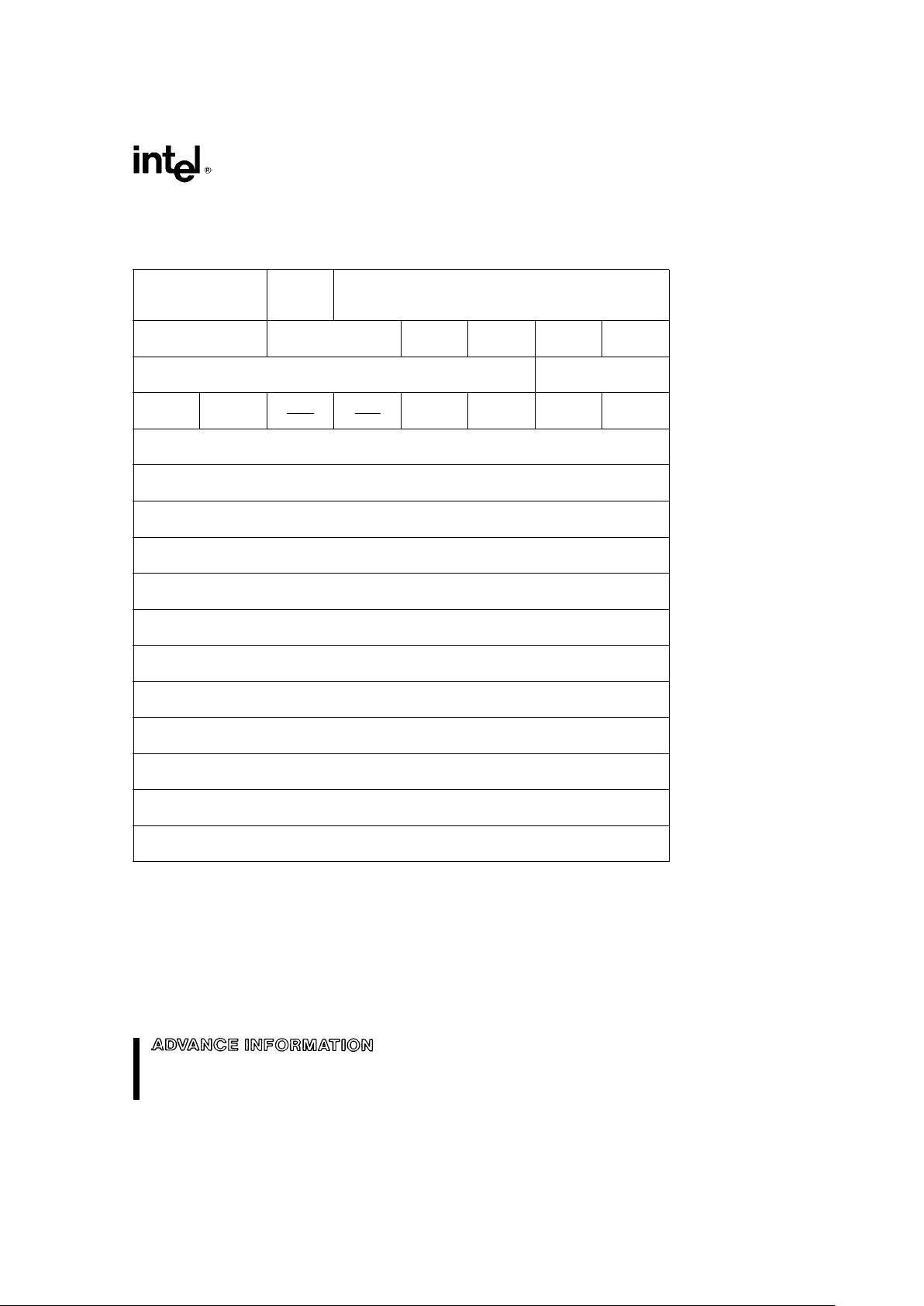
4.1.1 IO BANK 0
The format for IO Bank 0 is shown below.
76543210
Reg 0
POINTER ABORT COMMAND OP CODE (CMD
Reg)
RCV EXEC EXEC TX RX RX STP
States States INT INT INT INT Reg 1
ID REGISTER 0 0
(Counter) 1 (Auto En) 0 1 RESERVED Reg 2
0 0 Cur/ 32 IO/ EXEC TX RX RX STP
Resvrd Resvrd Base
HAR Mask Mask Mask Mask Reg 3
RCV CAR/BAR
(Low) Reg 4
RCV CAR/BAR
(High) Reg 5
RCV STOP REG
(Low) Reg 6
RCV STOP REG
(High) Reg 7
RCV Copy Threshold REG
Reg 8
EARLY XMT THRESHOLD REGISTER (XTR)
Reg 9
XMT CAR/BAR
(Low) Reg 10
XMT CAR/BAR
(High) Reg 11
Host Address Reg (Low)
/32-Bit I/O (Byte 0) Reg 12
Host Address Reg (High)
/32-Bit I/O (Byte 1) Reg 13
Local Memory I/O Port (Low)
/32-Bit I/O (Byte 2) Reg 14
Local Memory I/O Port (High)
/32-Bit I/O (Byte 3) Reg 15
15
82595FX
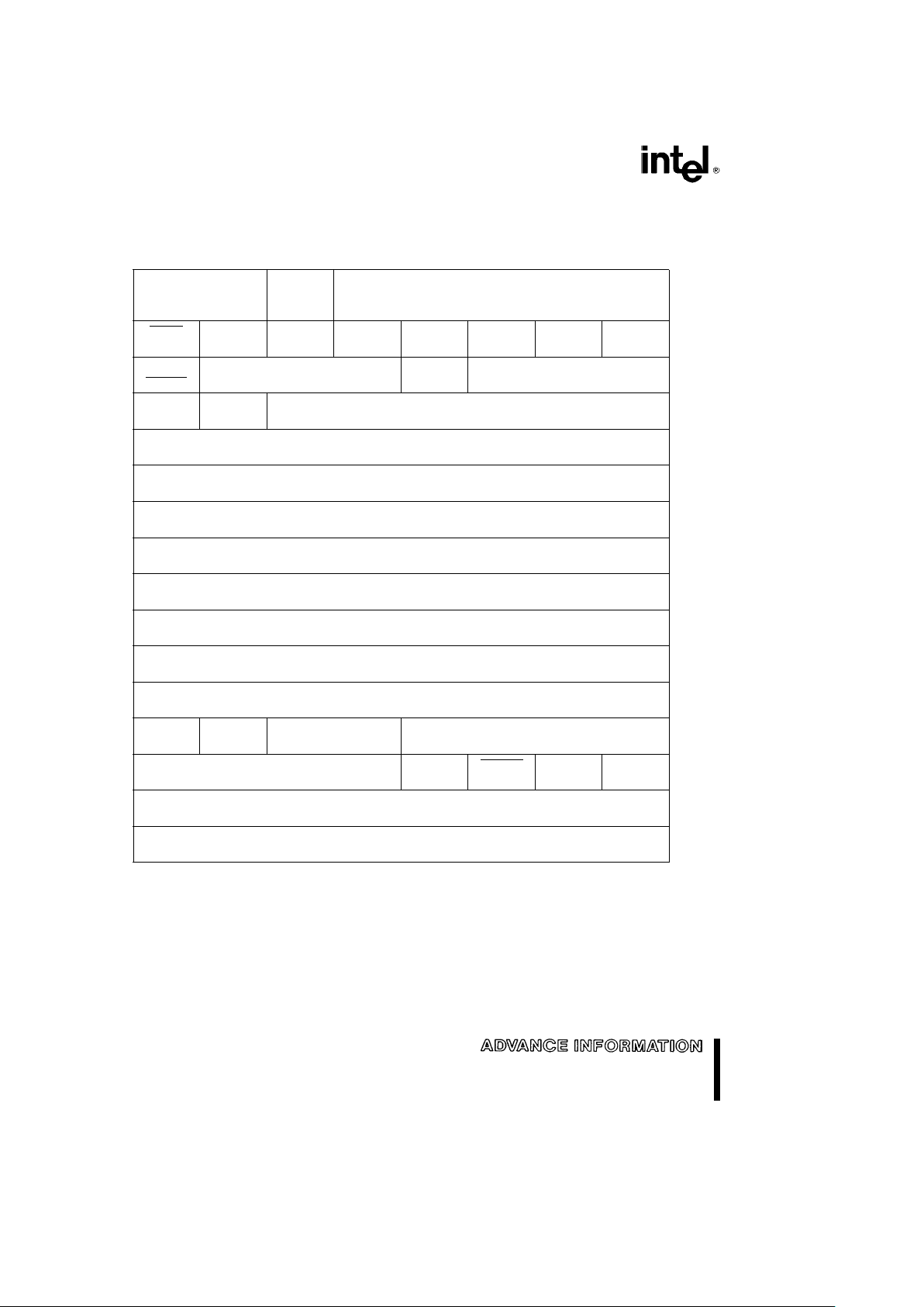
4.1.2 IO BANK 1
The format for IO Bank 1 is shown below.
76543210
Reg 0
POINTER ABORT COMMAND OP CODE (CMD
Reg)
Tri-ST 00000Host 0
INT Resvrd Resvrd Resvrd Resvrd Resvrd Bus Wd Resvrd Reg 1
FL/BT Boot EPROM/FLASH Bad
INT Select
Present Decode Window IRQ Reg 2
0 0 I/O Mapping
Window Reg 3
00000000
(Reserved) Reg 4
00000000
(Reserved) Reg 5
BACK TO BACK TRANSMIT IFS
Reg 6
RCV BOF Threshold REG
Reg 7
RCV LOWER LIMIT REG
(High Byte) Reg 8
RCV UPPER LIMIT REG
(High Byte) Reg 9
XMT LOWER LIMIT REG
(High Byte) Reg 10
XMT UPPER LIMIT REG
(High Byte) Reg 11
FLASH PAGE FLASH WRITE FLASH PAGE
SELECT HIGH ENABLE SELECT Reg 12
00000SMOUT 00
(Reserved) OUT EN Resvrd Resvrd Reg 13
00000000
(Reserved) Reg 14
00000000
(Reserved) Reg 15
16
82595FX
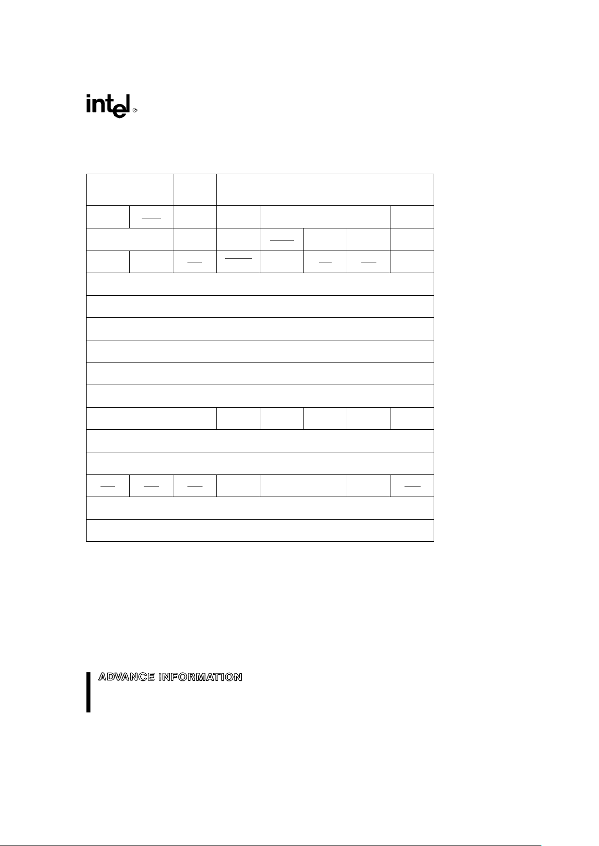
4.1.3 IO BANK 2
The format for IO Bank 2 is shown below.
76543210
Reg 0
POINTER ABORT COMMAND OP CODE (CMD
Reg)
Disc Tx Chn Tx Chn Res 0 0 0 TX Con
Bad Fr ErStp
Int Md 0 (Reserved) Proc En Reg 1
LoopBack
Multi No SA Length RX CRC BC PRMSC
IA Ins Enable In MEM DIS Mode Reg 2
Test 1 Test 2
BNC/
APORT
Jabber TPE/ Pol Link In
TPE
Disable AUI Corr Dis Reg 3
INDIVIDUAL ADDRESS
REGISTER 0 Reg 4
INDIVIDUAL ADDRESS
REGISTER 1 Reg 5
INDIVIDUAL ADDRESS
REGISTER 2 Reg 6
INDIVIDUAL ADDRESS
REGISTER 3 Reg 7
INDIVIDUAL ADDRESS
REGISTER 4 Reg 8
INDIVIDUAL ADDRESS
REGISTER 5 Reg 9
STEPPING
Turnoff
EEDO EEDI EECS EESK
Enable Reg 10
RCV NO RESOURCE
COUNTER Reg 11
Reserved
0 Reg 12
Polarity Link Activity 0 Auto-Negotiation A-N FDX/
LED
LED LED (Resvrd) Status Enable HDX Reg 13
00000000
(Reserved) Reg 14
00000000
(Reserved) Reg 15
4.2 Writing to the 82595FX
Writing to the 82595FX is accomplished by an IO
Write instruction (such as an OUT instruction) from
the host processor to one of the 82595FX registers.
The 82595FX registers reside in a block of 16 contiguous addresses contained within the PC IO address space. The mapping of this address block is
programmable throughout the 1 Kbyte PC IO address map.
The 82595FX registers are contained within three
banks of IO registers. When writing to a particular
register, the processor must first select the correct
bank (Bank 0, 1 or 2) in which the register resides.
Once a bank is selected, all register accesses are
made in that bank until a switch to another bank is
performed. Switching banks is accomplished by writing to the PTR field of Reg 0 in any bank. Reg 0 is
the command register of the 82595FX and its functionality is identical in each bank. Once in the appro-
17
 Loading...