
*Other brands and names are the property of their respective owners.
Information in this document is provided in connection with Intel products. Intel assumes no liability whatsoever, including infringement of any patent or
copyright, for sale and use of Intel products except as provided in Intel’s Terms and Conditions of Sale for such products. Intel retains the right to make
changes to these specifications at any time, without notice. Microcomputer Products may have minor variations to this specification known as errata.
October 1995COPYRIGHT©INTEL CORPORATION, 1996 Order Number: 290421-004
82503
DUAL SERIAL TRANSCEIVER (DST)
82503 PRODUCT FEATURE SET OVERVIEW
Y
Single Component Ethernet* Interface
to Both 802.3 10BASE-T and AUI
Y
Automatic or Manual Port Selection
Y
Manchester Encoder/Decoder and
Clock Recovery
Y
No Glue Interface to Industry-Standard
LAN Controllers
Ð Intel 82586, 82590, 82593 and 82596
Ð AMD 7990 (LANCE*)
Ð National Semiconductor 8390 and
83932 (SONIC*)
Ð Western Digital 83C690
Ð Fujitsu 86950 (Etherstar*)
Y
Diagnostic Loopback
Y
Reset, Low Power Modes
Y
Network Status Indicators
Y
Defeatable Jabber Timer
Y
User Test Modes
Y
10 MHz Transmit Clock Generator
Y
One Micron CHMOS** IV (Px48)
Technology
Y
Single 5-V Supply
INTERFACE FEATURES
TPE
Y
Complies with 10BASE-T, IEEE Std.
802.3i-1990 for Twisted Pair Ethernet
Y
Selectable Polarity Switching
Y
Direct Interface to TPE Analog Filters
Y
On-Chip TPE Squelch
Y
Defeatable Link Integrity (LI)
Y
Support of Cable Lengthsl100m
AUI
Y
Complies with IEEE 802.3 AUI Standard
Y
Direct Interface to AUI Transformers
Y
On-Chip AUI Squelch
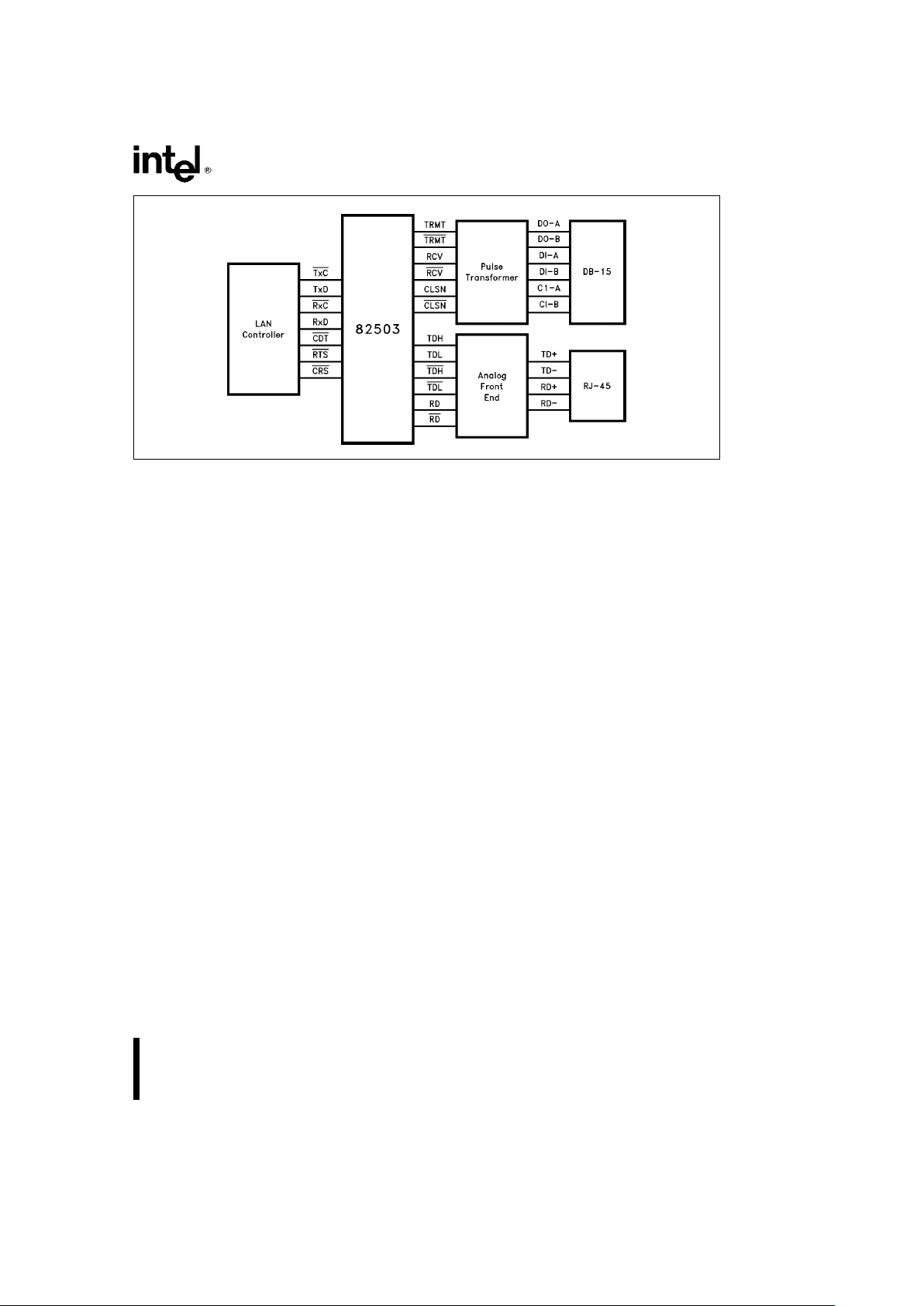
A block diagram of a typical application is shown in Figure 1. The 82503 Dual Serial Transceiver is a high-integration CMOS device designed to simplify interfacing industry standard Ethernet LAN Controllers to IEEE
802.3 local area network applications (10BASE5, 10BASE2, and 10BASE-T). The component supports both
an attachment unit interface (AUI) and a Twisted Pair Ethernet interface (TPE). It allows OEMs to design a
state-of-the-art media interface that is jumperless and fully automatic. The 82503 includes on-chip AUI and
TPE drivers and receivers; it offers designers a cost-effective, integrated solution for interfacing LAN controllers to the wire medium.
**CHMOS is a patented process of Intel Corporation.
*Ethernet is a registered trademark of Xerox Corporation.
LANCE is a registered trademark of Advanced Micro Devices.
Etherstar is a registered trademark of Fujitsu Electronics.
Sonic is a registered trademark of National Semiconductor Corporation.

82503 Dual Serial Transceiver (DST)
CONTENTS PAGE
1.0 82503 PRODUCT FEATURES
ААААААААА 3
2.0 PIN DEFINITION ААААААААААААААААААААААА 5
2.1 Power Pins АААААААААААААААААААААААААА 6
2.2 Clock Pins ААААААААААААААААААААААААААА 6
2.3 AUI Pins ААААААААААААААААААААААААААААА 6
2.4 TPE Pins АААААААААААААААААААААААААААА 7
2.5 Controller Interface Pins ААААААААААААА 7
2.6 Mode Pins ААААААААААААААААААААААААААА 8
2.7 LED Pins АААААААААААААААААААААААААААА 9
3.0 82503 ARCHITECTURE АААААААААААААА 10
3.1 Clock Generation ААААААААААААААААААА 10
3.2 Transmit Blocks АААААААААААААААААААА 10
3.3 Receive Blocks ААААААААААААААААААААА 11
3.4 Collision Detection ААААААААААААААААА 13
3.5 Link Integrity ААААААААААААААААААААААА 13
3.6 Jabber Function АААААААААААААААААААА 13
3.7 TPE Loopback ААААААААААААААААААААА 13
3.8 SQE Test Function ААААААААААААААААА 14
3.9 Port Selection АААААААААААААААААААААА 14
3.10 LED Description ААААААААААААААААААА 14
3.11 Polarity Switching ААААААААААААААААА 14
3.12 Controller Interface АААААААААААААААА 15
CONTENTS PAGE
4.0 RESET, LOW POWER AND TEST
MODES
АААААААААААААААААААААААААААААААА 16
4.1 Reset АААААААААААААААААААААААААААААА 16
4.2 Low Power and High Impedance
Modes
ААААААААААААААААААААААААААААААА 16
4.3 Diagnostic Loopback ААААААААААААААА 16
4.4 Customer Test Modes (Continuous
AUI/TPE Transmit) АААААААААААААААААА 16
5.0 APPLICATION EXAMPLE АААААААААААА 17
5.1 Introduction АААААААААААААААААААААААА 17
5.2 Design Guidelines АААААААААААААААААА 17
5.3 Layout Guidelines АААААААААААААААААА 17
6.0 PACKAGE THERMAL
SPECIFICATIONS АААААААААААААААААААААА 19
7.0 ELECTRICAL SPECIFICATIONS
AND TIMINGS АААААААААААААААААААААААААА 20
2
82503
290421– 1
Figure 1. Application Block Diagram
1.0 82503 PRODUCT FEATURES
The 82503 incorporates all the active circuitry required to interface Ethernet controllers to 10BASE-T
networks or the attachment unit interface (AUI). It
supports a direct no-glue interface to Intel’s family of
high-performance LAN controllers (82586, 82590,
82593, and 82596). The 82503 also provides a direct no-glue interface to the National Semiconductor
8390 and 83932 (SONIC), the Western Digital
83C690, the Advanced Micro Devices 7990
(LANCE) and 79C900 (ILACC), and the Fujitsu
86950 (Etherstar) controllers.
This component includes three advanced features:
jumperless two-port design capability, automatic port
selection, and polarity switching. The jumperless
TPE or AUI port selection capability allows designers maximum ease-of-use and network flexibility. Automatic port selection ensures complete software
compatibility with existing 10BASE2 and 10BASE5
software drivers. The 82503’s polarity switching feature will detect and correct polarity errors on the
twisted pairÐthe most common wiring fault in twisted pair networks.
The 82503 contains all the circuitry needed to meet
the 10BASE-T specification, including link integrity, a
jabber timer and internal predistortion. Deselecting
link integrity allows the component to be used in
some prestandard networks. The 82503’s jabber
timer prevents the station from continuously transmitting and is defeatable for simple design charac-
terization. The predistortion circuitry eliminates line
overcharge and reduces jitter on 10BASE-T links.
The 82503 can also support twisted pair cable
lengths of up to 200m when placed in TPE Extended
Squelch Mode (XSQ).
This component incorporates six LED drivers to display transmit data, receive data, collision, link integrity, polarity faults and port selections, allowing for
complete network monitoring by the user. The transmit, receive and collision LEDs indicate the rate of
activity by the frequency of flashing. The 82503 also
has a low power mode. During low power, many of
the 82503’s pins are in a high-impedance state to
facilitate board-level testing.
The 82503’s diagnostic loopback control enables it
to route a transmission signal from the LAN controller through its Manchester encoder-decoder circuitry
and back to the LAN controller. This provides effective network node fault detection and isolation capabilities. In addition, the 82503 supports diagnostic
test modes that generate continuous tranmission of
data through the twisted pair port, allowing designers to measure the analog performance of their design.
The 82503 is available in 44-lead PLCC and 44-lead
QFP packages and is fabricated with Intel’s lowpower, high-speed, CHMOS IV technology using a
single 5-V supply.
3
82503
290421– 2
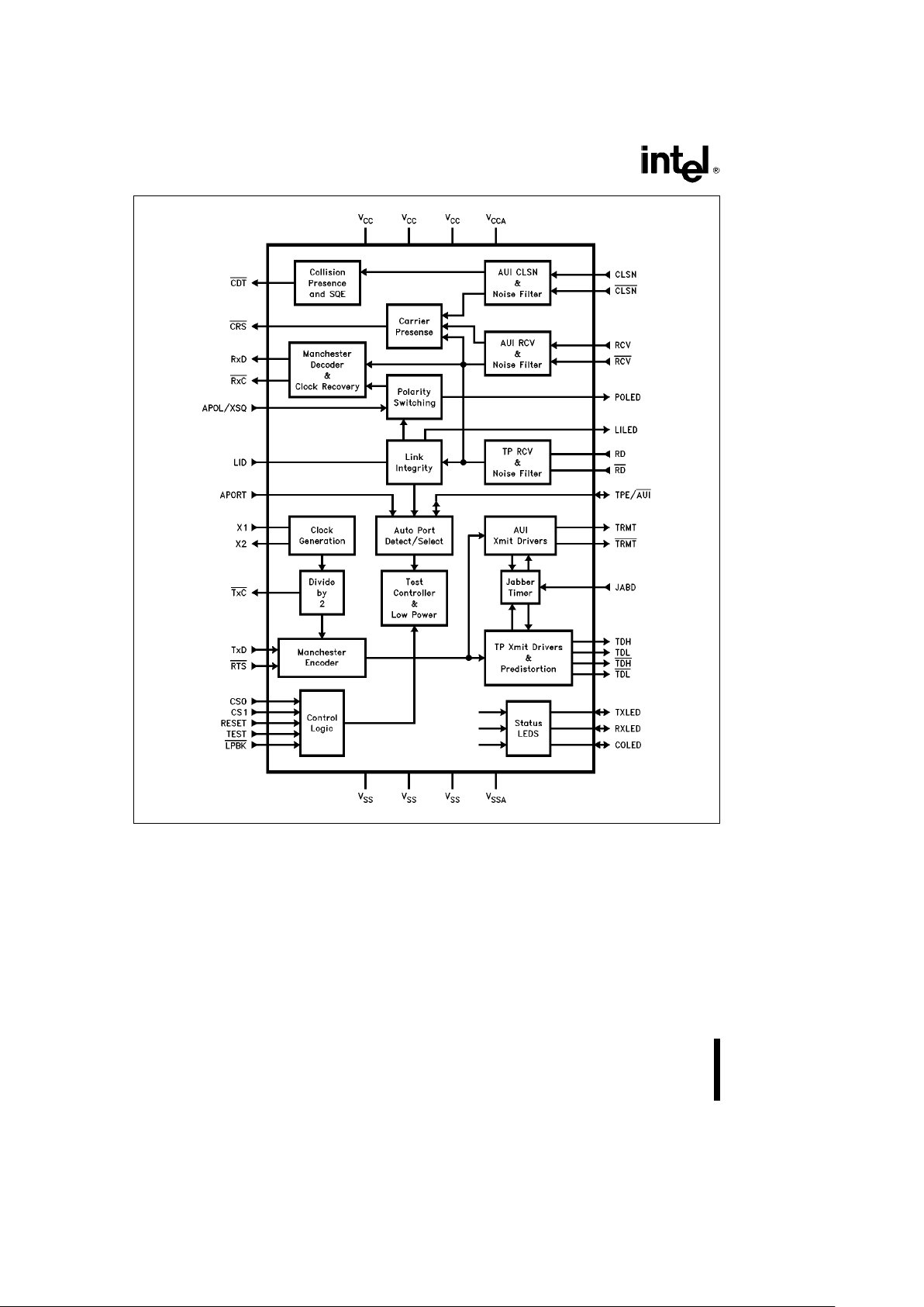
Figure 2. 82503 Functional Block Diagram
4
82503
2.0 PIN DEFINITION
290421– 3
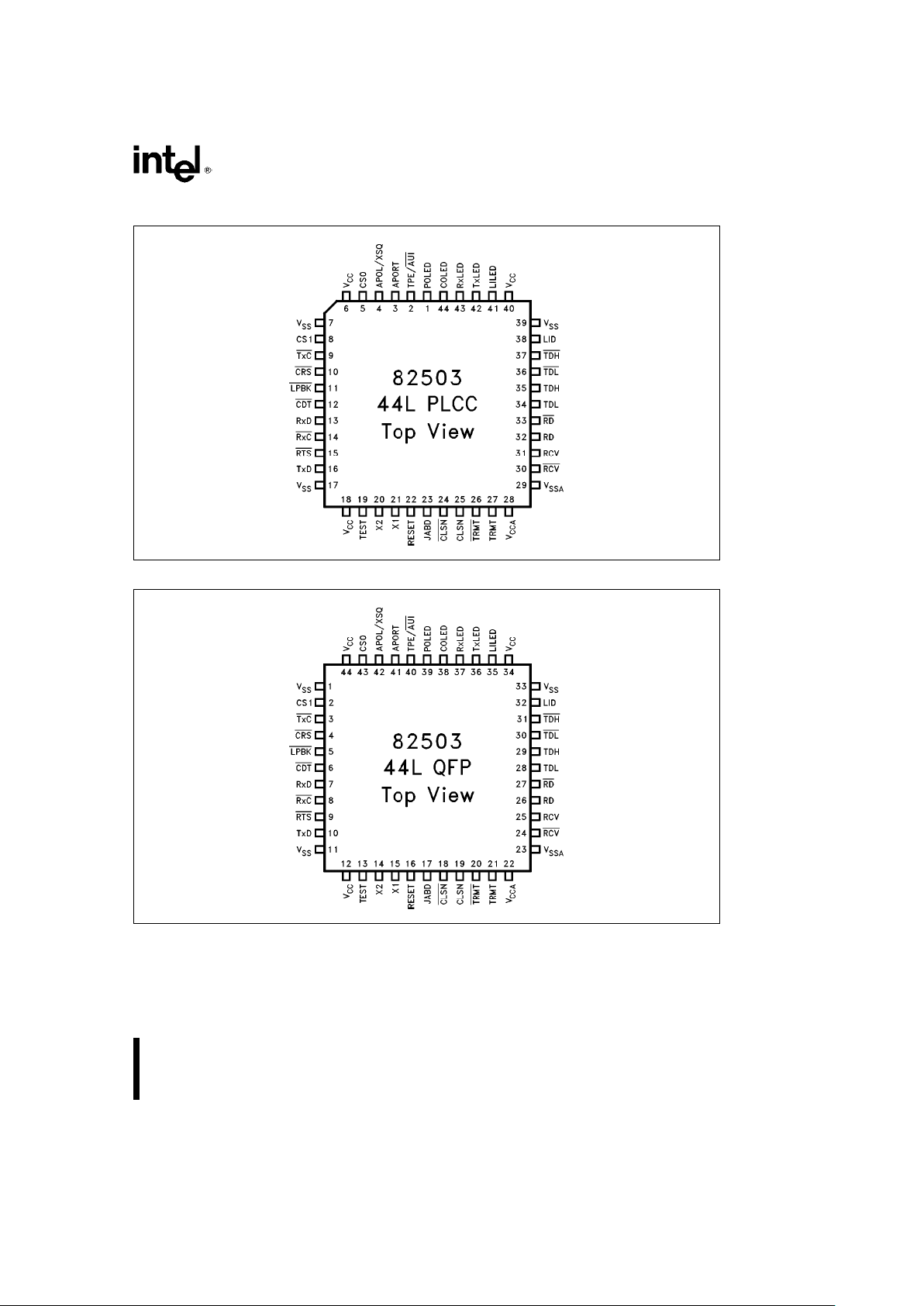
Figure 3. 44-Lead PLCC Pin Configuration
290421– 44
Figure 4. 44-Lead QFP Pin Configuration
5
82503
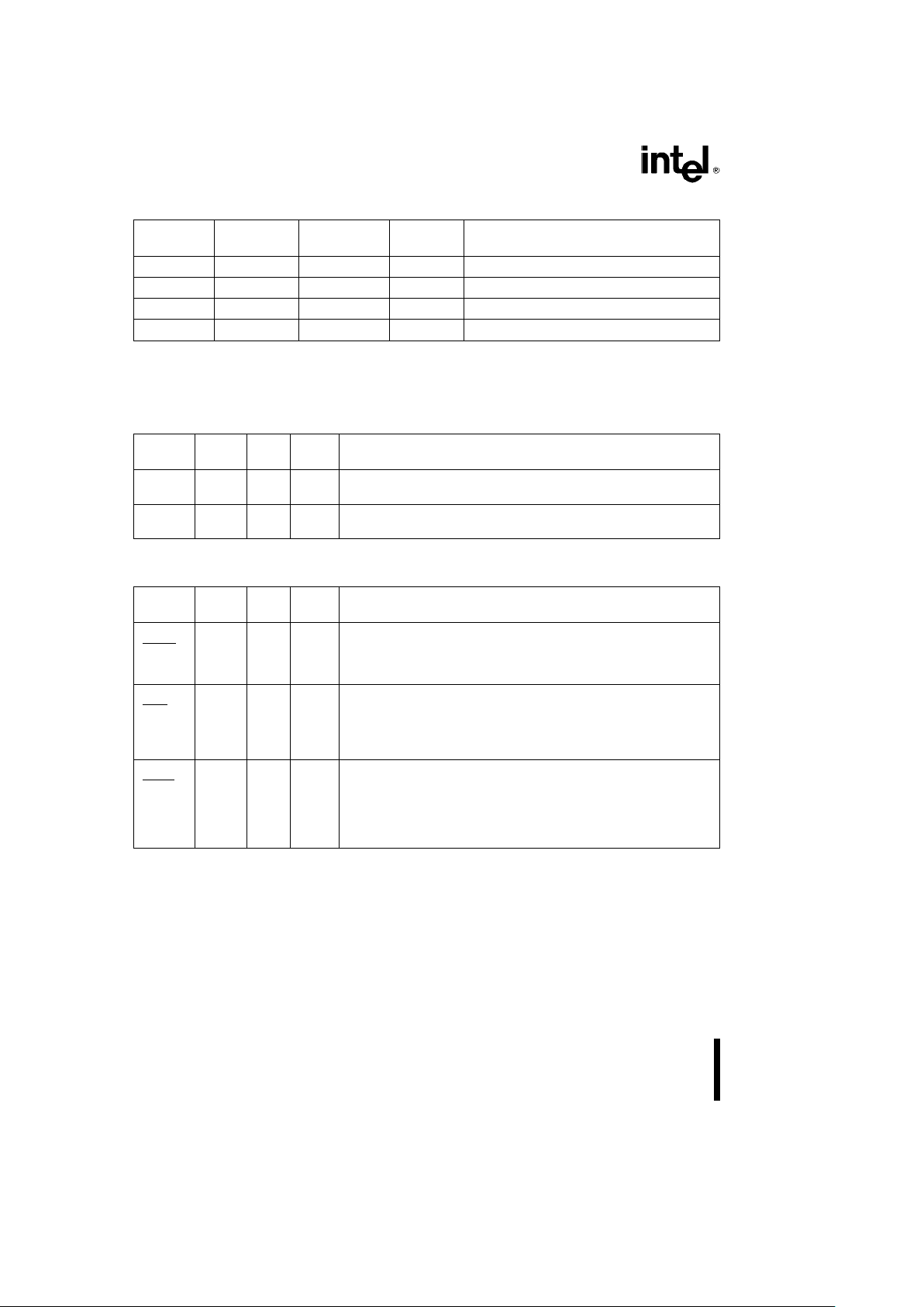
2.1 Power Pins
Symbol
PLCC QFP
Type Name and Function
Pin Pin
V
SS
(1)
7, 17, 39 1, 11, 33 Supply Digital Ground.
V
CC
(1)
6, 18, 40 44, 12, 34 Supply Digital VCC. A 5-Vg5% Power Supply.
V
CCA
(1)
28 22 Supply Analog VCC. A 5-Vg5% Power Supply.
V
SSA
(1)
29 23 Supply Analog Ground.
NOTE:
1. V
CC
and V
CCA
must be connected to the same power supply. VSSand V
SSA
must be connected to the same ground.
Separate decoupling and noise conditioning (e.g., ferrite beads) should be used.
2.2 Clock Pins
Symbol
PLCC QFP
Type Name and Function
Pin Pin
X1 21 15 I CLOCK CRYSTAL. A 20 MHz crystal input. This pin can be driven
with an external MOS level clock when X2 is left floating.
X2 20 14 O CLOCK CRYSTAL. A 20 MHz crystal output. X1 can be driven with
an external MOS level clock when this pin is left floating.
2.3 AUI Pins
Symbol
PLCC QFP
Type Name and Function
Pin Pin
TRMT 27 21 O TRANSMIT PAIR. A differential output driver pair that drives the
transmit pair of the transceiver cable. The output bit stream is
TRMT
26 20 O
Manchester encoded. Following the last transition, which is positive
at TRMT, the differential voltage is reduced to zero volts.
RCV 31 25 I RECEIVE PAIR. A differentially driven input pair which is tied to the
receive pair of the Ethernet transceiver cable. The first transition on
RCV
30 24 I
RCV is negative-going to indicate the beginning of the frame. The
last transition is positive-going to indicate the end of the frame. The
received bit stream is assumed to be Manchester encoded.
CLSN 25 19 I COLLISION PAIR. A differentially driven input pair tied to the
collision presence pair of the Ethernet transceiver cable. The
CLSN
24 18 I
collision presence signal is a 10 MHz square wave. The first
transition at CLSN is negative-going to indicate the beginning of the
signal; the last transition is positive-going to indicate the end of the
signal.
6

82503
2.4 TPE Pins
Symbol
PLCC QFP
Type Name and Function
Pin Pin
TDH 35 29 O TP TRANSMIT PAIR DRIVERS. These four outputs constitute the
twisted-pair drivers, which have predistortion capabilities. The TDH/
TDH
37 31 O
TDH outputs generate the 10 Mb/s Manchester Encoded data. The
TDL 34 28 O
TDL/TDL
outputs mirror the TDH/TDH outputs except for fat bit
TDL
36 30 O
occurrences (100 ns pulses). During the second half of a fat bit
(either high or low), the TDL/TDL outputs are inverted with respect
to TDH/TDH
outputs. This signal behavior reduces the amount of
jitter by preventing overcharge on the twisted pair medium.
RD 32 26 I TP RECEIVE PAIR. The differential twisted pair receiver. The
receiver pair is connected to the twisted pair medium and is driven
RD
33 27 I
with 10 Mb/s Manchester encoded data.
2.5 Controller Interface Pins
Symbol
PLCC QFP
Type Name and Function
Pin Pin
TxC 93OTRANSMIT CLOCK. A 10 MHz clock output tied directly to the
transmit clock pin of the Ethernet controller. Changes sense
depending on controller selected. Active low for Intel and Fujitsu
controller interfaces, active high for National and AMD interfaces.
Can drive one TTL load.
TxD 16 10 I TRANSMIT DATA. TTL input. NRZ serial data is clocked in on TxD
from the Ethernet controller. Connects directly to the transmit data
pin of the Ethernet controller.
RTS 15 9 I REQUEST TO SEND. TTL input. An active low input signal
synchronous to TxC
which enables data transmission on the active
port. Changes sense depending on controller selected. Active low
for the Intel controller interface, active high for National, AMD, and
Fujitsu interfaces.
RxC 14 8 O RECEIVE CLOCK. A 10 MHz clock output tied directly to the
receive clock pin of the Ethernet controller. This clock is the
recovered clock from incoming data on the active port. Changes
sense depending on controller selected. Active low for Intel and
Fujitsu controller interfaces, active high for National and AMD
interfaces. Can drive one TTL load.
RxD 13 7 O RECEIVE DATA. Received NRZ data (synchronous to RxC) passed
to the Ethernet controller. Connect directly to the receive data pin of
the controller. Can drive one TTL load.
CRS 10 4 O CARRIER SENSE. Output that alerts the Ethernet controller that
data is present on the active port. Connects directly to the carrier
sense pin of the Ethernet controller. Changes sense depending on
controller mode selected. Active low for Intel controller interface,
active high for National, AMD, and Fujitsu interfaces. Can drive one
TTL load.
CDT 12 6 O COLLISION DETECT. Output that indicates presence of a collision.
Connects directly to the collision detect pin of the Ethernet
controller. Changes sense depending on controller selected. Active
low for Intel and Fujitsu controller interfaces, active high for National
and AMD interfaces. Can drive one TTL load.
7

82503
2.6 Mode Pins
Symbol
PLCC QFP
Type Name and Function
Pin Pin
TPE/AUI 2 40 I/O PORT SELECT. TTL input/LED output. If APORT is low,
TPE/AUI
is an input and selects either the TPE port (TPE/AUI
high) or AUI port (TPE/AUI low). If APORT is high, the 82503 will
indicate the port selected by driving TPE/AUI
high (TPE) or low
(AUI). TPE/AUI
can drive an LED pull-up.
APORT 3 41 I AUTOMATIC PORT SELECTION. TTL input. When high, 82503
will automatically select TPE or AUI port based on presence of
valid link beats or frames on the TPE receive input. Mode
selected will be indicated on TPE/AUI
.
APOL/XSQ 4 42 I AUTOMATIC POLARITY CORRECTION/EXTENDED
SQUELCH ENABLE. TTL input. When high, the extended
squelch mode is disabled and automatic polarity correction is
enabled. Both junctions (APOL and XSQ) are enabled when this
pin is at a high impedance state. When low, both functions
become disabled. The presence of a polarity fault on the TPE
receive pair is indicated on POLED regardless of the state of
APOL.
LID 38 32 I LINK INTEGRITY DISABLE. TTL input. If high, link integrity
function is disabled. If low, link integrity function is enabled.
CS0 5 43 I CONTROLLER SELECT. Selects the appropriate interface for
the desired Ethernet controller. When CS0/1
e
0/0, supports
CS1 8 2 I
Intel controllers. When CS0/1
e
0/1, supports Fujitsu
controllers. When CS0/1
e
1/0, supports Western Digital and
National controllers. When CS0/1
e
1/1, supports AMD
controllers. (See Table 2.)
LPBK 11 5 I LOOPBACK. TTL input. An active low input signal that causes
the 82503 to enter diagnostic loopback mode. The twisted pair
or AUI medium will be removed from the circuit, thus isolating
the node from the network. When not connected, this pin
assumes the inactive (high) state. Diagnostic loopback does not
disable the operation of the link integrity processor, link beat
generator, or automatic port selection.
JABD 23 17 I JABBER DISABLE. TTL input. When high, this pin disables the
jabber function. When low, the jabber function is enabled and
the device performs AUI or TP jabber protection for the active
port. If this pin and TEST are asserted during a falling edge of
RESET, the 82503 enters its low power mode; when either this
pin or TEST deasserts, then the 82503 transitions to its normal
operating mode.
TEST 19 13 I TEST MODE ENABLE. TTL input. When TEST is high and
RESET is deasserted, a customer test mode is directly
accessed. When driven low, test mode is disabled. If this pin and
JABD are asserted during a falling edge of RESET, the 82503
enters its low power mode; when either this pin or JABD
deasserts, then the 82503 transitions to its normal operating
mode.
RESET 22 16 I RESET. TTL input. When high, resets internal circuitry. On the
falling edge of RESET, either test mode or low power mode can
be entered depending on the state of JABD and TEST.
8

82503
2.7 LED Pins
Symbol
PLCC QFP
Type Name and Function
Pin Pin
TxLED 42 36 I/O TRANSMIT LED. LED output. Indicates transmit status of the AUI or
TPE port. Normally off (high) output. Turns on to indicate
transmission. Flashes at a rate dependent on the level of transmit
activity. Upon entering a customer test mode, this pin must be
driven high either through an LED, or a resistor.
RxLED 43 37 I/O RECEIVE LED. LED output. Indicates receive status of the AUI or
TPE port. Normally off (high) output. Turns on to indicate reception.
Flashes at a rate dependent on the level of receive activity. Upon
entering a customer test mode, this pin must be driven high either
through an LED, or a resistor.
COLED 44 38 I/O COLLISION LED. LED output. Indicates collision status of the AUI
or TPE port. Normally off (high) output. Turns on to indicate
collision. Flashes at a rate dependent on the level of collision
activity. This pin is also used to determine which customer test
modes are entered.
LILED 41 35 O LINK INTEGRITY LED. LED output. Normally on (low) output which
indicates good link integrity on the TPE port during TPE mode.
Remains on when link integrity function has been disabled. Turns off
during AUI mode or when link integrity fails in TPE mode. Minimum
off time is 100 ms, minimum on time is set by the link integrity
function.
POLED 1 39 O POLARITY INDICATION. LED output. If the 82503 detects that the
receive TPE wires are reversed, POLED will turn on (low) to indicate
the fault. POLED remains on even if APOL/XSQ is high and the
82503 has automatically corrected for the reversed wires.
NOTE:
1. The LED outputs have a weak pull-up capable of sourcing 500 mA. They can sink 10 mA while still meeting TTL levels. All
LEDs can be used as indication pins if no LED is needed. Some of these outputs include pulse width conditioning, which
should be accounted for in software.
9

82503
3.0 82503 ARCHITECTURE
3.1 Clock Generation
A 20 MHz parallel resonant crystal is used to control
the clock generation oscillator, which provides the
basic 20 MHz clock source. An internal divide-bytwo counter generates the 10 MHz
g
0.01% clock
required by the IEEE 802.3 specification.
We recommend a crystal that meets the following
specifications be used.
#
Quartz Crystal
#
20 MHzg0.002% at 25§C
#
Accuracyg0.005% over full operating temperature, 0
§
Ctoa70§C
#
Parallel resonant with 20 pF Load Fundamental
Mode
#
Maximum Series Resistance: R
SERIES
e
30X
Several vendors have such crystals; either-off-the
shelf or custom made. Two possible vendors are:
1. M-Tron Industries, Inc.
Yankton, SD 57078
Specifications;
Part No. HC49 with 20 MHz, 50 PPM over 0
§
Cto
a
70§C, and 20 pF fundamental load.
2. Crystek Corporation
100 Crystal Drive
Ft. Myers, FL 33907
Part No. 013212
The accuracy of the Crystal Oscillator frequency depends on the PC board characteristics, therefore it is
advisable to keep the X1 and X2 traces as short as
possible. The optimum value of C1 and C2 should
be determined experimentally under nominal operating conditions. The typical value of C1 and C2 is
between 22 pF and 35 pF.
An external 20 MHz MOS-level clock may be applied
to pin X1, if pin X2 is left floating.
3.2 Transmit Blocks
3.2.1 MANCHESTER ENCODER
The 20 MHz clock is used to Manchester-encode
data on the TxD input. This clock is also divided by
two to produce the 10 MHz clock the LAN controller
needs for synchronizing its RTS
and TxD signals.
Data encoding and transmission begins with RTS
asserting. Since the first bit of a transmission is a 1,
the first transition is always negative on the transmit
outputs (TRMT or TD pins). Transmission ends
when RTS
deasserts. The last transition is always
positive at the transmit outputs (TRMT or TD pins)
and may occur at the center of the bit cell if the last
data bit to be transmitted is a 1, or at the boundary
of the bit cell if the last data bit to be sent is a 0.
Immediately after the end of a transmission, all signals on the RCV pair (when AUI mode is selected)
are inhibited for 4 to 5 ms. This dead time is necessary for proper operation of the SQE (heartbeat)
test.
3.2.2 AUI CABLE DRIVER
The AUI cable driver (TRMT pair) is a differential
circuit, which interfaces to the AUI cable through a
pulse transformer.
High voltage protection is achieved by using a transformer to isolate the transmit pins (TRMT pair) from
the transceiver cable. The total transmit circuit inductance, including the 802.3 transceiver transformers, should be a minimum of 27 mH for Ethernet applications.
3.2.3 TWISTED PAIR CABLE DRIVER
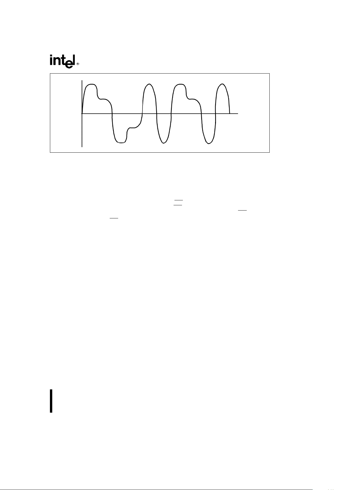
The twisted pair line drivers (TD pairs) begin transmitting the serial Manchester bit stream 3 bit times
after RTS
is asserted. The line drivers use a predistortion algorithm to improve jitter performance for up
to 100 meters of twisted pair cable. The line drivers
reduce their drive level during the second half of
‘‘fat’’ (100 ns) Manchester pulses and maintain a full
drive level during all ‘‘thin’’ (50 ns) pulses and during
the first half of the ‘‘fat’’ pulses. This reduces line
overcharging during ‘‘fat’’ pulses, a major source of
jitter.
10
82503
290421– 4
Figure 5. TPE Predistortion
3.3 Receive Blocks
3.3.1 MANCHESTER DECODER AND CLOCK
RECOVERY
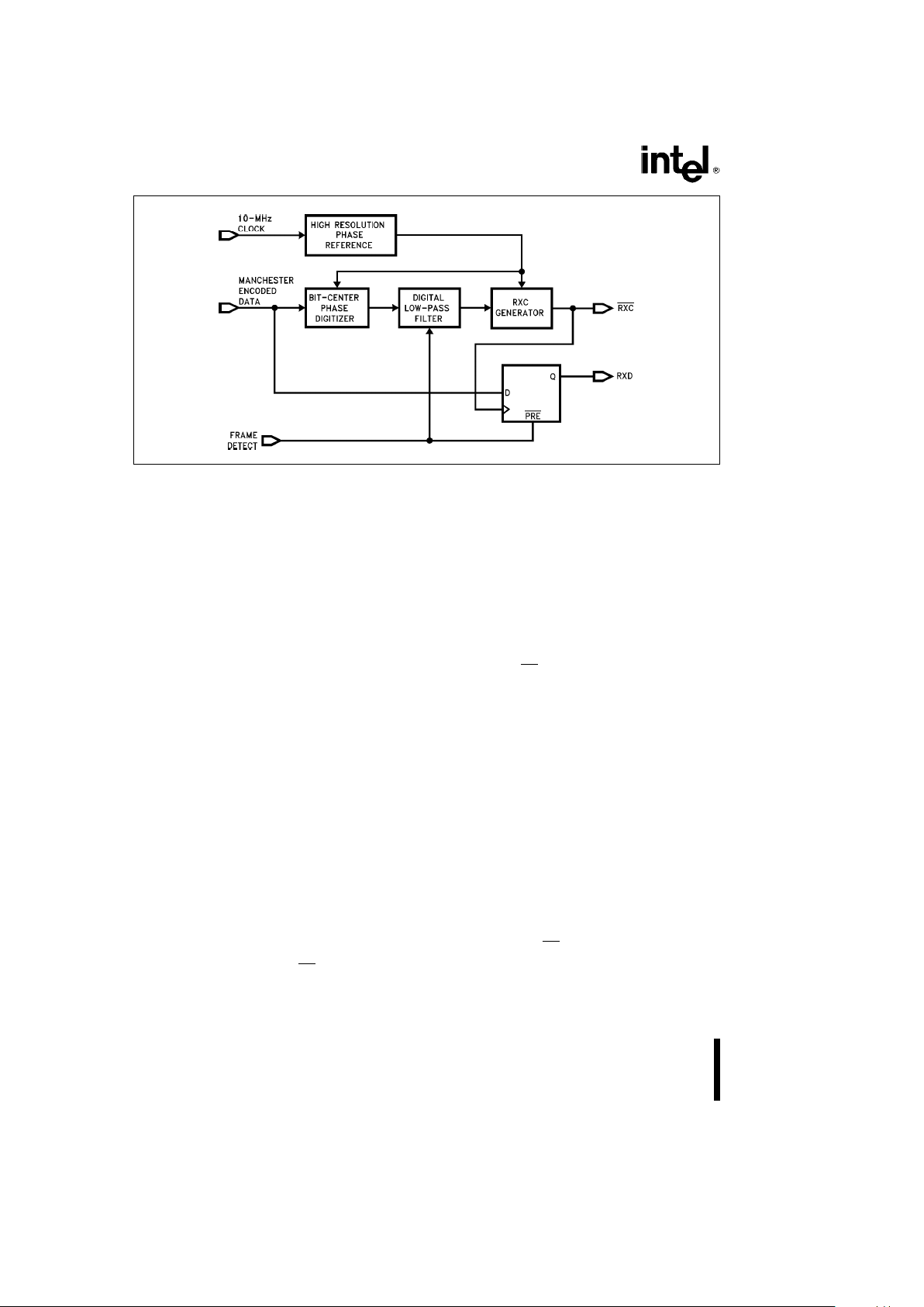
The 82503 performs Manchester decoding and timing recovery of the incoming data in AUI and TPE
modes.
The Manchester-encoded data stream is decoded to
separate the Receive Clock (RxC
) and the Receive
Data (RxD) from the differential signal. The 82503
uses an advanced digital technique to perform the
decoding function. The use of digital circuitry instead
of analog circuitry (e.g., a phase-lock loop) to perform the decoding ensures that the decoding function is less sensitive to variations in operating conditions.
A high-resolution phase reference is used to digitize
the phase of the incoming data bit-center transition.
The digitizer has a phase resolution of 1/32 of a bit
time.
The digitized phase is filtered by a digital low-pass
filter to remove rapid phase variations, i.e., phase
jitter. Slow phase variations, such as those caused
by small differences between the data frequency
and the clock frequency, are not filtered by the lowpass filter.
The RxC generator digitally sets the phases of the
two RxC
transitions to respectively lead and lag the
bit-center transition by (/4 bit time. RxC
is used to
recover RxD by sampling the incoming data with an
edge-triggered flip-flop.
Lock is achieved by reducing the time constant of
the digital filter to zero at the start of a new frame.
Any uncertainty in the bit-center phase of the first
transition that is caused by jitter is subsequently removed by gradually increasing the filter time constant during the following preamble. By that time, the
phase of the bit center is output by the filter, and
lock is achieved. Lock is achieved within the first 14
bit times as seen by the AUI inputs. The maximum
bit-cell timing distortion (jitter) tolerated by the Manchester decoder circuitry is
g
12 ns (preamble),
g
18 ns (data) for AUI, andg13.5 ns for TPE (data
and preamble).
11
82503
290421– 5
Figure 6. Manchester Decoder and Clock Recovery
3.3.2 AUI RECEIVE AND COLLISION BUFFERS
The AUI receive and collision inputs are driven
through isolation transformers to provide high voltage protection and DC common mode voltage rejection. The incoming signals are converted to digital
levels and passed to the Manchester decoder and
collision detection circuitry.
3.3.3 AUI RECEIVE AND COLLISION
SQUELCH CIRCUITS
Both the receive (RCV) and collision (CLSN) pairs
have the following squelch characteristics.
#
The squelch circuits are turned on at idle.
#
A pulse is rejected if the peak differential voltage
is more positive than
b
160 mV regardless of
pulse width.
#
A pulse is considered valid if its peak differential
voltage is more negative than
b
300 mV and its
width, measured at
b
285 mV, is greater than
25 ns.
#
The squelch circuits are disabled by the first valid
negative differential pulse on either the AUI receive (RCV) or the AUI collision (CLSN) pair.
#
If a positive differential pulse occurs on either the
AUI receive or collision pairs for greater than
160 ns, End of Frame (EOF) is assumed and the
squelch circuitry is turned on.
3.3.4 TPE RECEIVE BUFFER
The TPE receive pins (RD and RD
) are connected to
the twisted pair medium through an analog front
end. The analog front end contains the line coupling
devices and EMI filters necessary to conform to the
10BASE-T standards and local RF regulations. The
input differential voltage range for the TPE receiver
is greater than 500 mV and less than 3.1V differential.
3.3.5 TPE RECEIVE SQUELCH CIRCUITS
The TPE receive buffer distinguishes valid receive
differential data, link test pulses, and the idle condition according to the requirements of the 10BASE-T
standard. Signals at the output of the EMI filter (thus
at the RD and RD
pair) are rejected as follows:
#
All differential pulses of peak magnitude less than
300 mV are rejected.
#
All continuous sinusoids with a differential amplitude less than 6.2 V
PP
and a frequency less than
2 MHz are rejected.
#
All sine waves of single cycle duration starting
with phase 0
§
or 180§that have an amplitude less
than 6.2 V
PP
, and a frequency of 2 MHz to
16 MHz are rejected, if the single cycle is preceeded and followed by 4 bit times of silence
(i.e., a signal less than 300 mV).
3.3.6 TPE Extended Squelch Mode
By placing the 82503 into TPE extended squelch
mode, the 82503 can support cable lengths greater
than the 100m specified in the 10Base-T IEEE standard (802.3i-1990). The squelch thresholds for the
signals at the RD/RD
pair are typically reduced by
4.5 dB. This allows Grade 5 twisted-pair cable to be
used to overcome attenuation and multipair crosstalk for cable lengths up to 200 meters.
12

82503
TPE extended squelch mode is enabled by presenting a high-impedance (
l
100 KX) at the APOL/XSQ
pin. This can be done by floating the APOL/XSQ pin,
tying APOL/XSQ low through a 100 K X resistor, or
driving APOL/XSQ with a three-state buffer. When
driven high or low using a TTL driver or a low impedance pull-up or pull-down (
k
2KX) extended
squelch is disabled and the driven level at the
APOL/XSQ pin determines the state of the polaritycorrection function (APOL/XSQ
e
1 enables polari-
ty correction, APOL/XSQ
e
0 disables polarity correction). The TPE extended squelch feature is transparent to previous steppings of the 82503. Polarity
correction is always enabled when the TPE extended-squelch feature is enabled (APOL/XSQ
e
Z).
The APOL/XSQ pin senses a high-impedance state
by an active-polling circuit implemented at the pin.
Two small polling devices attempt to pull the APOL/
XSQ pin up to V
CC
and down to VSS. If the pin is in a
high-impedance state, the devices will be successful
in pulling the APOL/XSQ pin high and low. If the pin
is driven high or low, the polling devices will not be
able to successfully pull the pin in the opposite direction. In this way, an internal state machine can
correctly determine one of three states of the
APOL/XSQ pin. The pin is polled every 25.6 ms.
3.4 Collision Detection
3.4.1 AUI COLLISION DETECTION
Collision detection in the AUI mode is performed by
the attached transceiver, and signalled to the 82503
on the CLSN pair. A 10 MHz
a
25%, orb15%,
square wave with transition times between 35 ns
and 70 ns indicates the collision. The 82503 reports
this to the LAN controller on the CDT
pin.
3.4.2 TPE COLLISION DETECTION
Collision detection in the TPE mode is indicated by
simultaneous transmission and reception on the
twisted pair link segment. The CDT
signal is assert-
ed for the duration of both RTS
and the presence of
received data; CRS
is asserted for the duration of
either RTS
or the presence of received data. During
a collision, the source of RxD will be the received
data. If the received data stream ends before the
transmit data stream, the RxD source will be
changed to transmit data stream until it ends.
3.5 Link Integrity
The 82503 supports the link integrity function as defined by 10BASE-T. During long periods of idle on
the transmitter, link test pulses will be transmitted on
to the twisted pair medium as an indication to the
remote MAU that the link is good. These pulses will
be transmitted 8 ms to 24 ms after the end of the
last transmission or link test pulse.
The link integrity function continuously monitors activity on the receive circuit. If neither valid data nor
link test pulses are received, the link integrity processor declares the link bad, and disables transmission and reception on the media, loopback, and the
SQE test function. Transmission of link test pulses
and monitoring receive activity are not affected. The
idle time required for the link integrity processor to
determine the link is bad is 50 ms to 150 ms.
Once a frame or a sequence of 2 to 10 valid consecutive link test pulses are detected, the Link Integrity
Processor declares the link is good, and reconnects
the transmitter and receiver.
The link integrity function can be disabled by driving
the LID pin high or by disabling automatic port selection (APORT
e
0) and selecting the AUI port. This
option is intended primarily for use with pre10BASE-T networks.
3.6 Jabber Function
The 82503 contains a jabber timer to implement the
jabber function. If a transmission continues beyond
the limits specified, the jabber function inhibits further transmission and asserts the collision indicator,
CDT. The limits for jabber transmission are 20 ms to
150 ms in TPE Mode, and 8 ms to 16 ms in AUI
mode. For both AUI and TPE mode, the transmission inhibit period extends until the 82503 detects
sufficient idle time (between 250 ms and 750 ns) on
the RTS
signal. The jabber function can be disabled
by driving the JABD high.
In TPE mode the link integrity function continues to
operate even if the jabber function is inhibiting transmission. Link test pulses continue to be sent and the
receive circuit continues to be monitored. Additionally, the link integrity function reconnects to a restored
link without waiting for the transmit input to go idle
when the jabber function is inhibiting transmission.
3.7 TPE Loopback
In TPE mode the 82503 implements the transmit to
receive loopback (DO to DI) mode specified in the
10BASE-T standard. This mode loops back transmitted data through the receive path.
This function is required to maintain full compatibility
with coax MAUs where the data loopback is a natural result of the architecture.
13
82503
The transmit to receive loopback function is disabled
when the jabber function or link integrity function is
inhibiting transmission.
3.8 SQE Test Function
The 82503 supports the SQE test function when in
TPE mode or in Diagnostic Loopback mode. The
82503 will assert its CDT
pin within 0.6 msto1.6ms
after the end of a transmission, and it will remain
asserted for 5- to 15-bit times. If the 82503 is in the
TPE mode and is not in diagnostic loopback mode,
the link integrity function will disable the SQE test
function when it detects a bad link.
3.9 Port Selection
The 82503 features both manual and automatic port
selection. To enable automatic port selection, connect APORT to V
CC
. The 82503 then starts in TPE
mode and monitors link integrity. If the link is good,
the 82503 stays in TPE mode and pulls TPE/AUI
high to indicate that the TPE port was selected. If
link integrity fails, the 82503 switches to AUI mode
and pulls TPE/AUI
low to indicate that the AUI port
is now active. TPE/AUI
can drive an LED to indicate
port selection (on for AUI, off for TPE mode). Note
that LILED will be on if TPE mode is selected and off
if AUI mode is selected. If link integrity is disabled
while automatic port selection is enabled, the 82503
defaults to TPE mode. If the 82503 changes ports
while RTS
is active, transmission is terminated with
an End of Frame marker on the old port. Transmission of the remaining packet fragment is not allowed
on the new port. Transmissions will begin with a
complete data packet.
The port can be manually selected by driving
APORT low. TPE/AUI
e
0 selects AUI mode, and
TPE/AUI
e
1 TPE mode. When the port is manually
selected, the circuitry for the unused port is powered
down. Changing ports requires 100 ms to allow the
circuitry for the new port to resume normal operation.
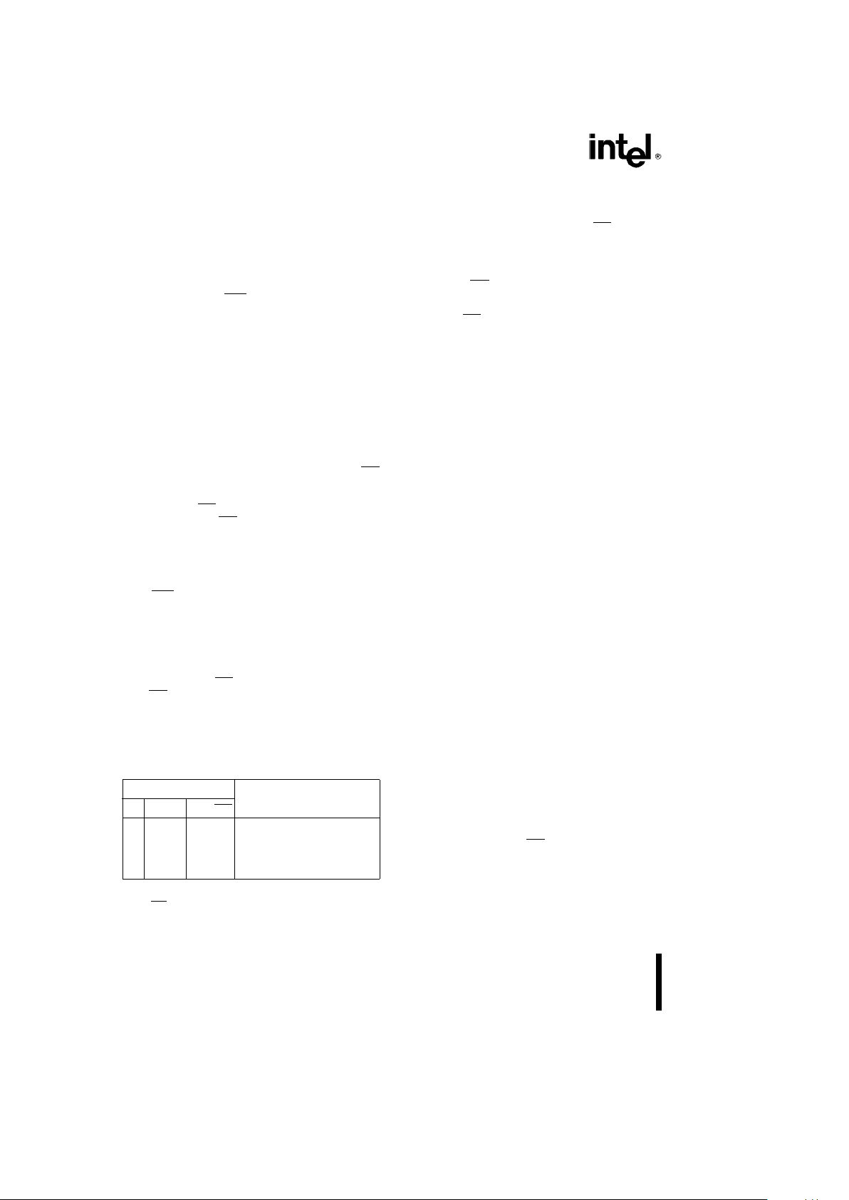
Table 1. Port Selection
Configuration
State
LID APORT TPE/AUI
X 0 0 AUI (TPE Port Powered Down)
X 0 1 TPE (AUI Port Powered Down)
01 X*Automatic Port Selection
11 X*TPE
NOTE:
*TPE/AUI
is an output pin when APORTe1.
3.10 LED Description
The 82503 supports six LED pins to indicate the
status of important states; TPE/AUI
, TxLED,
POLED, LILED, RxLED, COLED. Each pin is capable
of directly driving an LED.
3.10.1 TPE/AUI
When automatic port selection is enabled (APORT is
high), TPE/AUI
becomes an LED output and turns
off if TPE mode is selected and on if AUI mode is
selected.
3.10.2 TxLED
Transmit status. This LED is normally off and flashes
at 2.5 Hz, 5 Hz, and 10 Hz to indicate respectively a
low, medium, and high rate of transmit activity.
3.10.3 RxLED
Receive LED. This LED is normally off and flashes at
2.5 Hz, 5 Hz, and 10 Hz to indicate respectively a
low, medium, and high rate of receive activity.
3.10.4 COLED
Collision LED. This LED is normally off and flashes
at 2.5 Hz, 5 Hz, and 10 Hz to indicate respectively a
low, medium, and high rate of collision activity.
3.10.5 POLED
Polarity Fault. This LED is normally off and turns on
to indicate a polarity fault in the receive pair of the
10BASE-T link. Operation of this pin is not affected
by the state of the polarity correction function
(APOL/XSQ
e
X).
3.10.6 LILED
Link Integrity status. When Aport is enabled
(APORT
e
1), this LED is normally on (driven low)
to indicate the presence of a valid 10BASE-T link
when the TPE port is active. The LED will turn off
(driven high) when the link fails. When link integrity is
disabled (LID
e
1) while APORT is enabled
(APORT
e
1) this LED is turned on (driven low). If
APORT is disabled (APORT
e
0) and the AUI port is
manually selected (TPE/AUI
e
0) the LED output is
tristated.
3.11 Polarity Switching
In TPE mode, the 82503 monitors receive link beats
and end-of-frame delimiters for a possible receiver
14
 Loading...