*Other brands and names are the property of their respective owners.
Information in this document is provided in connection with Intel products. Intel assumes no liability whatsoever, including infringement of any patent or
copyright, for sale and use of Intel products except as provided in Intel’s Terms and Conditions of Sale for such products. Intel retains the right to make
changes to these specifications at any time, without notice. Microcomputer Products may have minor variations to this specification known as errata.
April 1994COPYRIGHT©INTEL CORPORATION, 1995 Order Number: 270946-005
8XC196MC
INDUSTRIAL MOTOR CONTROL
MICROCONTROLLER
87C196MC 16 Kbytes of On-Chip OTPROM*
87C196MC, ROM 16 Kbytes of On-Chip Factory-Programmed OTPROM
80C196MC ROMless
Y
High-Performance CHMOS 16-Bit CPU
Y
16 Kbytes of On-Chip OTPROM/
Factory-Programmed OTPROM
Y
488 bytes of On-Chip Register RAM
Y
Register to Register Architecture
Y
Up to 53 I/O Lines
Y
Peripheral Transaction Server (PTS)
with 11 Prioritized Sources
Y
Event Processor Array (EPA)
Ð 4 High Speed Capture/Compare
Modules
Ð 4 High Speed Compare Modules
Y
Extended Temperature Standard
Y
Two 16-Bit Timers with Quadrature
Decoder Input
Y
3-Phase Complementary Waveform
Generator
Y
13 Channel 8/10-Bit A/D with Sample/
Hold with Zero Offset Adjustment H/W
Y
14 Prioritized Interrupt Sources
Y
Flexible 8-/16-Bit External Bus
Y
1.75 ms 16 x 16 Multiply
Y
3 ms 32/16 Divide
Y
Idle and Power Down Modes
The 8XC196MC is a 16-bit microcontroller designed primarily to control 3 phase AC induction and DC brushless motors. The 8XC196MC is based on Intel’s MCS
É
96 16-bit microcontroller architecture and is manufac-
tured with Intel’s CHMOS process.
The 8XC196MC has a three phase waveform generator specifically designed for use in ‘‘Inverter’’ motor
control applications. This peripheral allows for pulse width modulation, three phase sine wave generation with
minimal CPU intervention. It generates 3 complementary non-overlapping PWM pulses with resolutions of
0.125 ms (edge trigger) or 0.250 m s (centered).
The 8XC196MC has 16 Kbytes on-chip OTPROM/ROM and 488 bytes of on-chip RAM. It is available in three
packages; PLCC (84-L), SDIP (64-L) and EIAJ/QFP (80-L).
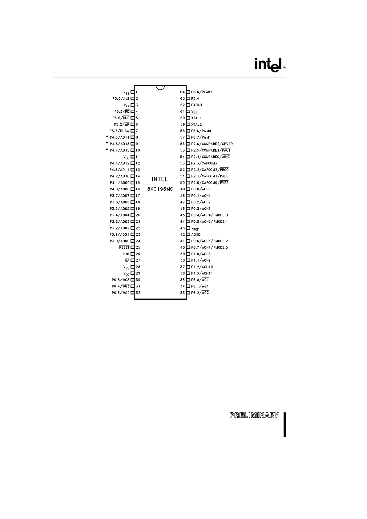
Note that the 64-L SDIP package does not include P1.4, P2.7, P5.1 and the CLKOUT pins.
Operational characteristics are guaranteed over the temperature range of
b
40§Ctoa85§C.
The 87C196MC contains 16 Kbytes on-chip OTPROM. The 83C196MC contains 16 Kbytes on-chip ROM. All
references to the 80C196MC also refers to the 83C196MC and 87C196MC unless noted.
*OTPROM (One Time Programmable Read Only Memory) is the same as EPROM but it comes in an unwindowed package
and cannot be erased. It is user programmable.

8XC196MC
270946– 1
NOTE:
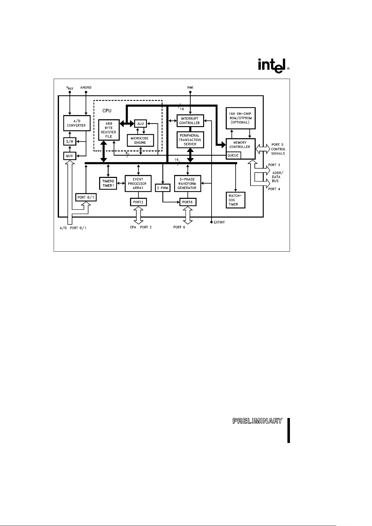
Connections between the standard I/O ports and the bus are not shown.
Figure 1. 87C196MC Block Diagram
2

8XC196MC
PROCESS INFORMATION
This device is manufactured on PX29.5, a CHMOS
III-E process. Additional process and reliability information is available in Intel’s
Components Quality
and Reliability Handbook,
Order Number 210997.
270946– 16
EXAMPLE: N87C196MC is 84-Lead PLCC OTPROM,
16 MHz.
For complete package dimensional data, refer to the
Intel Packaging Handbook (Order Number 240800).
NOTE:
1. EPROMs are available as One Time Programmable
(OTPROM) only.
Figure 3. The 8XC196MC Family Nomenclature
Thermal Characteristics
Package
i
ja
i
jc
Type
PLCC 35§C/W 13§C/W
QFP 56§C/W 12§C/W
SDIP TBD TBD
All thermal impedance data is approximate for static air
conditions at 1W of power dissipation. Values will change
depending on operation conditions and application. See
the Intel
Packaging Handbook
(order number 240800) for a
description of Intel’s thermal impedance test methodology.
8XC196MC Memory Map
Description Address
External Memory or I/O 0FFFFH
06000H
Internal ROM/EPROM or External 5FFFH
Memory (Determined by EA
)
2080H
Reserved. Must contain FFH. 207FH
(Note 5)
205EH
PTS Vectors 205DH
2040H
Upper Interrupt Vectors 203FH
2030H
ROM/EPROM Security Key 202FH
2020H
Reserved. Must contain FFH. 201FH
(Note 5)
201CH
Reserved. Must Contain 20H 201BH
(Note 5)
CCB1 201AH
Reserved. Must Contain 20H 2019H
(Note 5)
CCB0 2018H
Reserved. Must contain FFH. 2017H
(Note 5)
2014H
Lower Interrupt Vectors 2013H
2000H
SFR’s 1FFFH
1F00H
External Memory 1EFFH
0200H
488 Bytes Register RAM (Note 1) 01FFH
0018H
CPU SFR’s (Notes 1, 3) 0017H
0000H
NOTES:
1. Code executed in locations 0000H to 03FFH will be
forced external.
2. Reserved memory locations must contain 0FFH unless
noted.
3. Reserved SFR bit locations must contain 0.
4. Refer to 8XC196KC for SFR descriptions.
5. WARNING: Reserved memory locations must not be
written or read. The contents and/or function of these locations may change with future revisions of the device.
Therefore, a program that relies on one or more of these
locations may not function properly.
3

8XC196MC
270946– 2
NOTE:
*The pin sequence is correct.
The 64-Lead SDIP package does not include the following pins: P1.4/ACH12, P2.7/COMPARE3, P5.1/INST,
CLKOUT.
Figure 2. 64-Lead Shrink DIP (SDIP) Package
4

8XC196MC
270946– 3
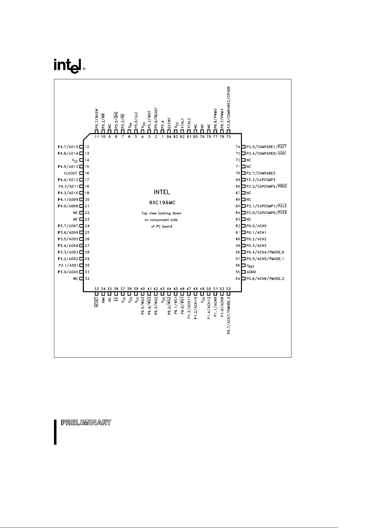
NOTE:
NC means No Connect. Do not connect these pins.
Figure 3. 84-Lead PLCC Package
5

8XC196MC
270946– 4
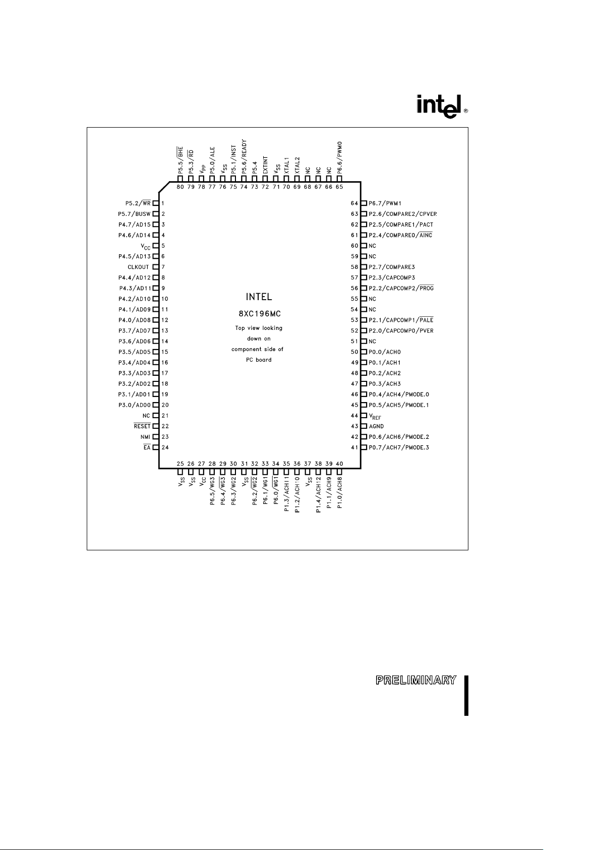
NOTE:
NC means No Connect. Do not connect these pins.
Figure 4. 80-Lead Shrink EIAJQFP (Quad Flat Pack)
6

8XC196MC
PIN DESCRIPTIONS (Alphabetically Ordered)
Symbol Function
ACH0–ACH12 Analog inputs to the on-chip A/D converter. ACH0–7 share the input pins
(P0.0–P0.7, P1.0 – P1.4)
with P0.0 – 7 and ACH8 –12 share pins with P1.0 – 4. If the A/D is not used,
the port pins can be used as standard input ports.
ANGND Reference ground for the A/D converter. Must be held at nominally the
same potential as V
SS
.
ALE/ADV(P5.0) Address Latch Enable or Address Valid output, as selected by CCR. Both
options allow a latch to demultiplex the address/data bus on the signal’s
falling edge. When the pin is ADV
, it goes inactive (high) at the end of the
bus cycle. ALE/ADV
is active only during external memory accesses. Can be
used as standard I/O when not used as ALE/ADV.
BHE/WRH (P5.5) Byte High Enable or Write High output, as selected by the CCR. BHE will go
low for external writes to the high byte of the data bus. WRH
will go low for
external writes where an odd byte is being written. BHE
/WRH is activated
only during external memory writes.
BUSWIDTH (P5.7) Input for bus width selection. If CCR bits 1 and 2e1, this pin dynamically
controls the bus width of the bus cycle in progress. If BUSWIDTH is low, an
8-bit cycle occurs. If it is high, a 16-bit cycle occurs. This pin can be used as
standard I/O when not used as BUSWIDTH.
CAPCOMP0–CAPCOMP3 The EPA Capture/Compare pins. These pins share P2.0 – P2.3. If not used
(P2.0–P2.3)
for the EPA, they can be configured as standard I/O pins.
CLKOUT Output of the internal clock generator. The frequency is (/2 of the oscillator
frequency. It has a 50% duty cycle.
COMPARE0–COMPARE3 The EPA Compare pins. These pins share P2.4 – P2.7. If not used for the
(P2.4–P2.7)
EPA, they can be configured as standard I/O pins.
EA External Access enable pin. EAe0 causes all memory accesses to be
external to the chip. EA
e
1 causes memory accesses from location 2000H
to 5FFFH to be from the on-chip OTPROM/QROM. EA
e
12.5V causes
execution to begin in the programming mode. EA
is latched at reset.
EXTINT A programmable input on this pin causes a maskable interrupt vector
through memory location 203CH. The input may be selected to be a
positive/negative edge or a high/low level using WGÐPROTECT (1FCEH).
INST (P5.1) INST is high during the instruction fetch from the external memory and
throughout the bus cycle. It is low otherwise. This pin can be configured as
standard I/O if not used as INST.
NMI A positive transition on this pin causes a non-maskable interrupt which
vectors to memory location 203EH. If not used, it should be tied to VSS. May
be used by Intel Evaluation boards.
PORT0 8-bit high impedance input-only port. Also used as A/D converter inputs.
Port0 pins should not be left floating. These pins also used to select
programming modes in the OTPROM devices.
PORT1 5-bit high impedance input-only port. P1.0–P1.4 are also used as A/D
converter inputs. In addition, P1.2 and P1.3 can be used as Timer 1 clock
input and direction select respectively.
PORT2 8-bit bidirectional I/O port. All of the Port2 pins are shared with the EPA I/O
pins (CAPCOMP0 – 3 and COMPARE0 –3).
PORT3 8-bit bidirectional I/O ports with open drain outputs. These pins are shared
PORT4
with the multiplexed address/data bus which uses strong internal pullups.
PORT5 8-bit bidirectional I/O port. 7 of the pins are shared with bus control signals
(ALE
, INST, WR,RD, BHE, READY, BUSWIDTH). Can be used as standard
I/O.
7
 Loading...