

*Other brands and names are the property of their respective owners.
Information in this document is provided in connection with Intel products. Intel assumes no liability whatsoever, including infringement of any patent or
copyright, for sale and use of Intel products except as provided in Intel’s Terms and Conditions of Sale for such products. Intel retains the right to make
changes to these specifications at any time, without notice. Microcomputer Products may have minor variations to this specification known as errata.
November 1994
COPYRIGHT
©
INTEL CORPORATION, 1995
Order Number: 272430-002
80186/80188
HIGH-INTEGRATION 16-BIT MICROPROCESSORS
Y
Integrated Feature Set
Ð Enhanced 8086-2 CPU
Ð Clock Generator
Ð 2 Independent DMA Channels
Ð Programmable Interrupt Controller
Ð 3 Programmable 16-bit Timers
Ð Programmable Memory and
Peripheral Chip-Select Logic
Ð Programmable Wait State Generator
Ð Local Bus Controller
Y
Available in 10 MHz and 8 MHz
Versions
Y
High-Performance Processor
Ð 4 Mbyte/Sec Bus Bandwidth
Interface
@
8 MHz (80186)
Ð 5 Mbyte/Sec Bus Bandwidth
Interface
@
10 MHz (80186)
Y
Direct Addressing Capability to 1 Mbyte
of Memory and 64 Kbyte I/O
Y
Completely Object Code Compatible
with All Existing 8086, 8088 Software
Ð 10 New Instruction Types
Y
Numerics Coprocessing Capability
Through 8087 Interface
Y
Available in 68 Pin:
Ð Plastic Leaded Chip Carrier (PLCC)
Ð Ceramic Pin Grid Array (PGA)
Ð Ceramic Leadless Chip Carrier (LCC)
Y
Available in EXPRESS
Ð Standard Temperature with Burn-In
Ð Extended Temperature Range
(
b
40§Ctoa85§C)
272430– 1
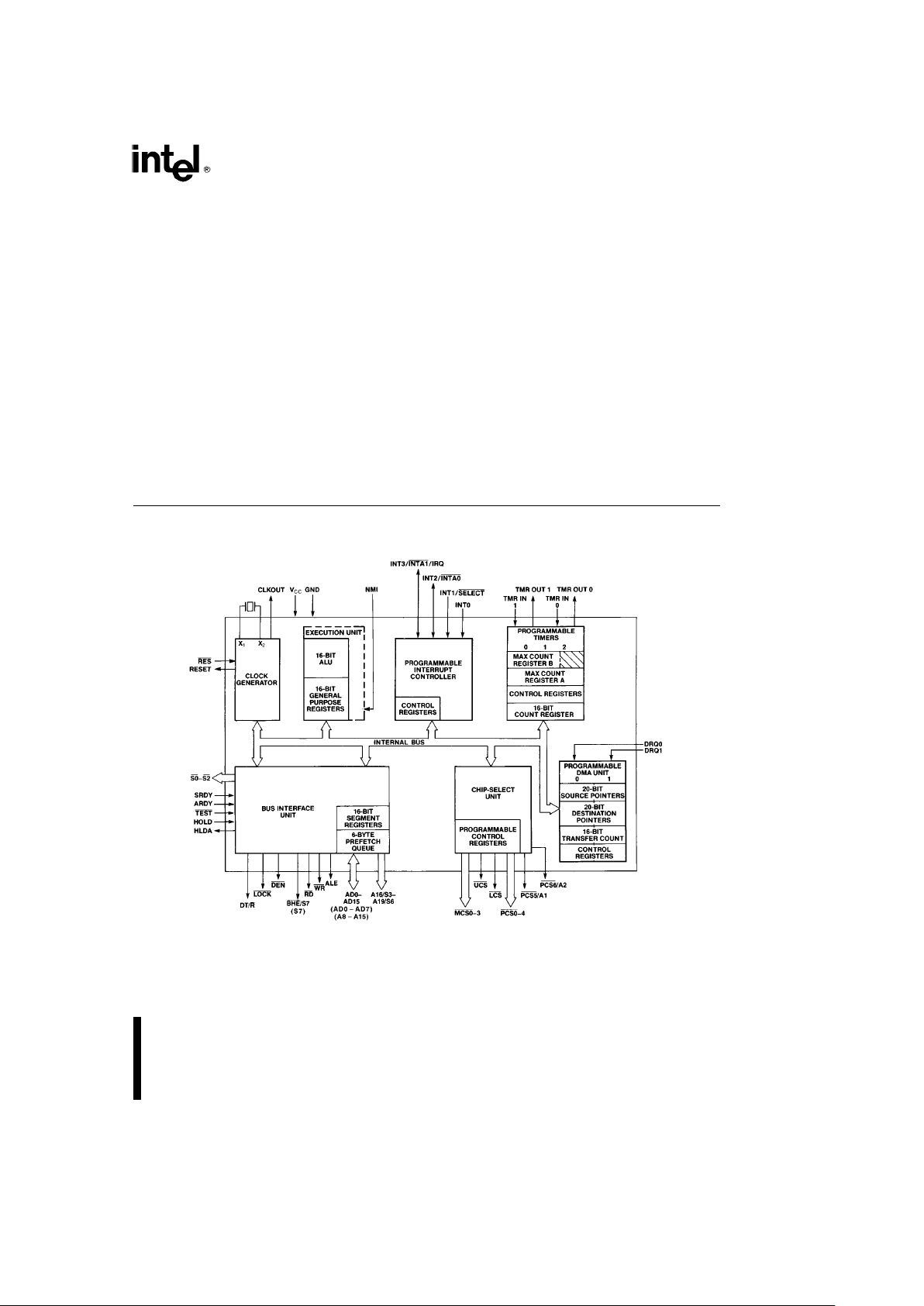
Figure 1. Block Diagram
1

80186/80188 High-Integration 16-Bit Microprocessors
CONTENTS PAGE
FUNCTIONAL DESCRIPTION
ААААААААААААА 9
Introduction АААААААААААААААААААААААААААААААА 9
CLOCK GENERATOR ААААААААААААААААААААА 9
Oscillator АААААААААААААААААААААААААААААААААА 9
Clock Generator ААААААААААААААААААААААААААА 9
READY Synchronization АААААААААААААААААААА 9
RESET Logic ААААААААААААААААААААААААААААААА 9
LOCAL BUS CONTROLLER ААААААААААААААА 9
Memory/Peripheral Control ААААААААААААААА 10
Local Bus Arbitration АААААААААААААААААААААА 10
Local Bus Controller and Reset АААААААААААА 10
PERIPHERAL ARCHITECTURE АААААААААА 10
Chip-Select/Ready Generation Logic АААААА 10
DMA Channels АААААААААААААААААААААААААААА 11
Timers АААААААААААААААААААААААААААААААААААА 11
Interrupt Controller АААААААААААААААААААААААА 12
CONTENTS PAGE
ABSOLUTE MAXIMUM RATINGS
АААААААА 15
D.C. CHARACTERISTICS АААААААААААААААА 15
A.C. CHARACTERISTICS АААААААААААААААА 16
EXPLANATION OF THE AC
SYMBOLS
АААААААААААААААААААААААААААААА 18
WAVEFORMS АААААААААААААААААААААААААААА 19
EXPRESS АААААААААААААААААААААААААААААААА 25
EXECUTION TIMINGS ААААААААААААААААААА 26
INSTRUCTION SET SUMMARY АААААААААА 27
FOOTNOTES ААААААААААААААААААААААААААААА 32
REVISION HISTORY ААААААААААААААААААААА 33
2
2
80186/80188
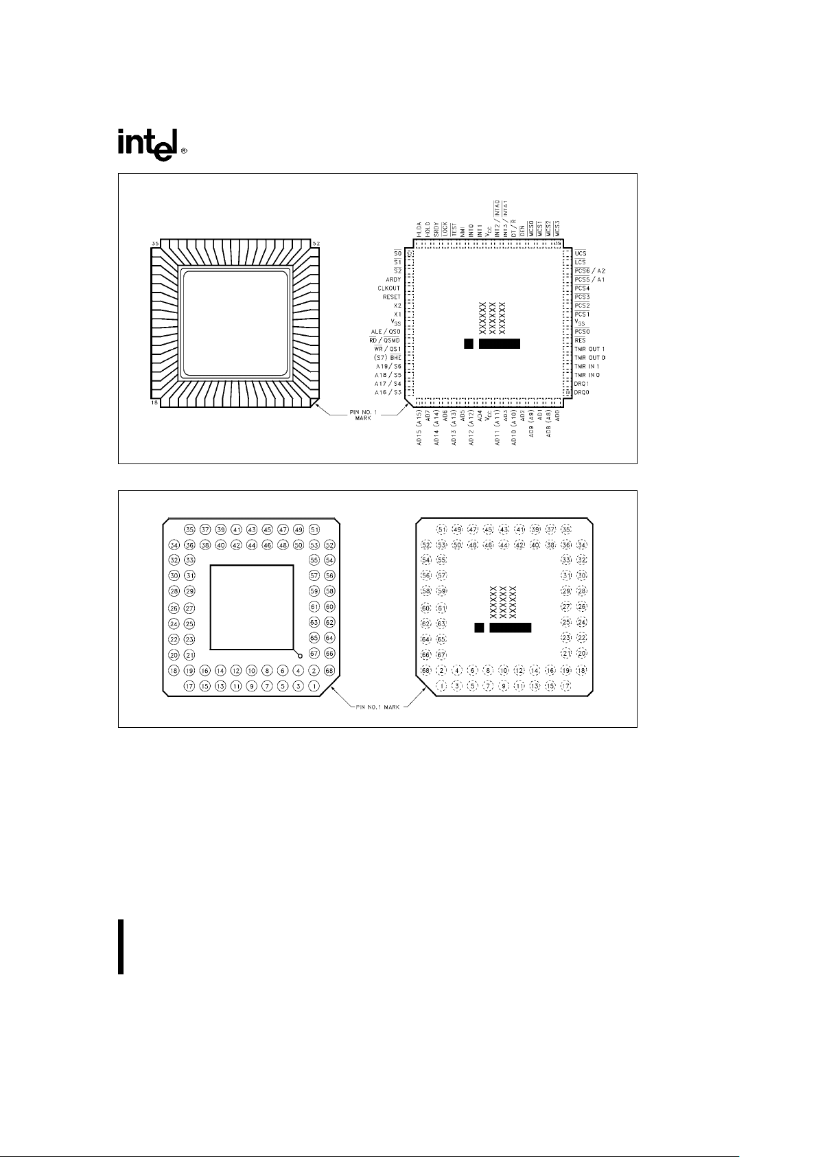
Contacts Facing Up
Contacts Facing Down
272430– 2
Figure 2. Ceramic Leadless Chip Carrier (JEDEC Type A)
Pins Facing Up Pins Facing Down
272430– 3
Figure 3. Ceramic Pin Grid Array
NOTE:
Pin names in parentheses apply to the 80188.
3
3
80186/80188
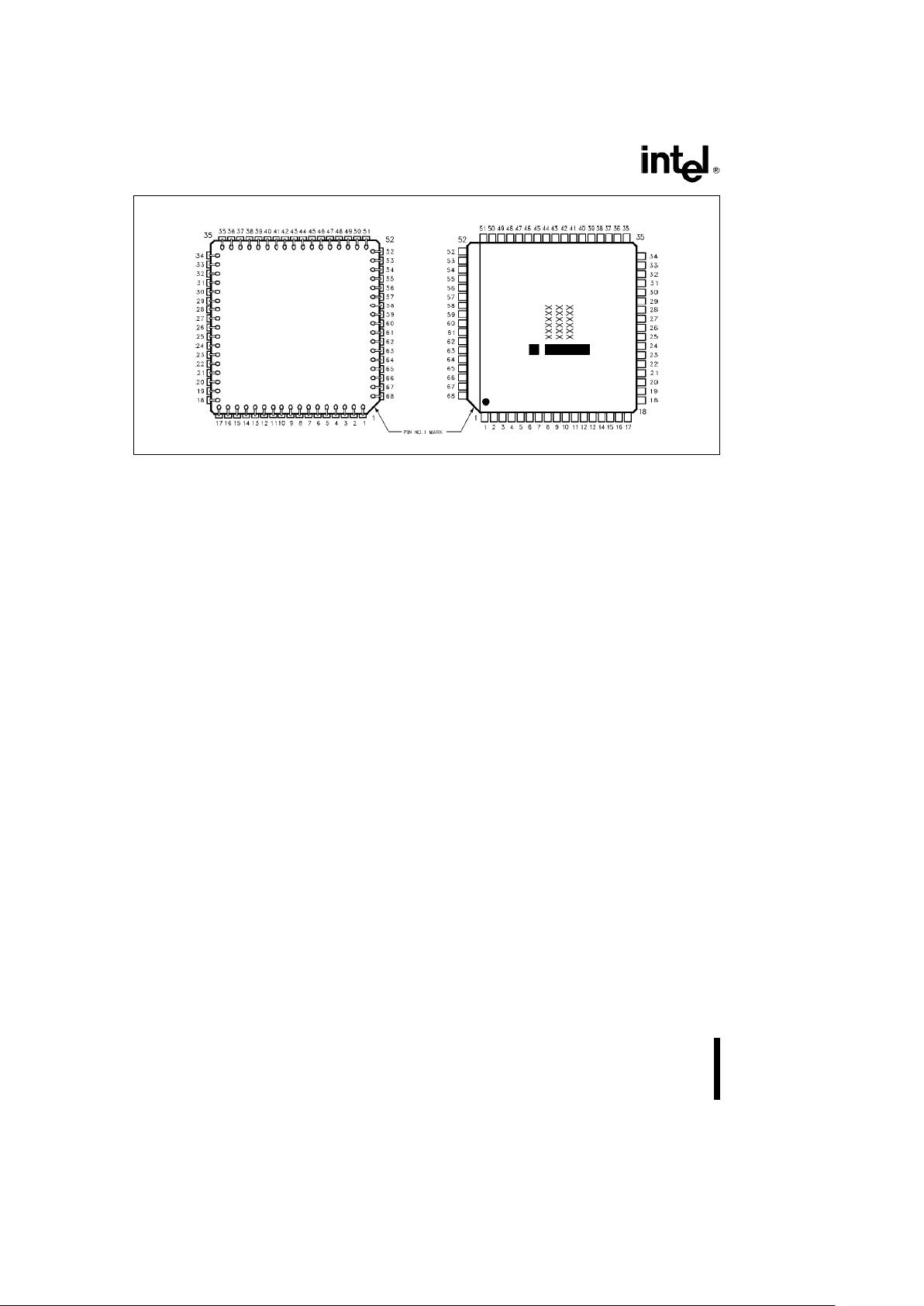
Leads Facing Up Leads Facing Down
272430– 4
Figure 4. Plastic Leaded Chip Carrier
NOTE:
Pin names in parentheses apply to the 80188.
4
4
80186/80188
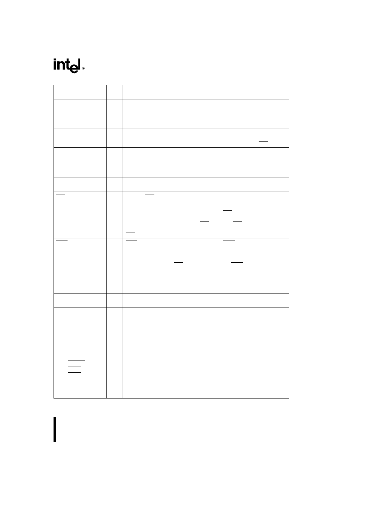
Table 1. Pin Descriptions
Symbol
Pin
Type Name and Function
No.
V
CC
9ISYSTEM POWER:a5 volt power supply.
43
V
SS
26 I System Ground.
60
RESET 57 O Reset Output indicates that the CPU is being reset, and can be used as a system
reset. It is active HIGH, synchronized with the processor clock, and lasts an
integer number of clock periods corresponding to the length of the RES
signal.
X1 59 I Crystal Inputs X1 and X2 provide external connections for a fundamental mode
parallel resonant crystal for the internal oscillator. Instead of using a crystal, an
X2 58 O
external clock may be applied to X1 while minimizing stray capacitance on X2.
The input or oscillator frequency is internally divided by two to generate the
clock signal (CLKOUT).
CLKOUT 56 O Clock Output provides the system with a 50% duty cycle waveform. All device
pin timings are specified relative to CLKOUT.
RES 24 I An active RES causes the processor to immediately terminate its present
activity, clear the internal logic, and enter a dormant state. This signal may be
asynchronous to the processor clock. The processor begins fetching
instructions approximately 6(/2 clock cycles after RES
is returned HIGH. For
proper initialization, VCCmust be within specifications and the clock signal must
be stable for more than 4 clocks with RES
held LOW. RES is internally
synchronized. This input is provided with a Schmitt-trigger to facilitate power-on
RES
generation via an RC network.
TEST 47 I/O TEST is examined by the WAIT instruction. If the TEST input is HIGH when
‘‘WAIT’’ execution begins, instruction execution will suspend. TEST
will be
resampled until it goes LOW, at which time execution will resume. If interrupts
are enabled while the processor is waiting for TEST, interrupts will be serviced.
During power-up, active RES
is required to configure TEST as an input. This pin
is synchronized internally.
TMR IN 0 20 I Timer Inputs are used either as clock or control signals, depending upon the
programmed timer mode. These inputs are active HIGH (or LOW-to-HIGH
TMR IN 1 21 I
transitions are counted) and internally synchronized.
TMR OUT 0 22 O Timer outputs are used to provide single pulse or continous waveform
generation, depending upon the timer mode selected.
TMR OUT 1 23 O
DRQ0 18 I DMA Request is asserted HIGH by an external device when it is ready for DMA
Channel 0 or 1 to perform a transfer. These signals are level-triggered and
DRQ1 19 I
internally synchronized.
NMI 46 I The Non-Maskable Interrupt input causes a Type 2 interrupt. An NMI transition
from LOW to HIGH is latched and synchronized internally, and initiates the
interrupt at the next instruction boundary. NMI must be asserted for at least one
clock. The Non-Maskable Interrupt cannot be avoided by programming.
INT0 45 I Maskable Interrupt Requests can be requested by activating one of these pins.
When configured as inputs, these pins are active HIGH. Interrupt Requests are
INT1/SELECT
44 I
synchronized internally. INT2 and INT3 may be configured to provide active-
INT2/INTA0
42 I/O
LOW interrupt-acknowledge output signals. All interrupt inputs may be
INT3/INTA1
/IRQ 41 I/O
configured to be either edge- or level-triggered. To ensure recognition, all
interrupt requests must remain active until the interrupt is acknowledged. When
Slave Mode is selected, the function of these pins changes (see Interrupt
Controller section of this data sheet).
NOTE:
Pin names in parentheses apply to the 80188.
5
5
80186/80188
Table 1. Pin Descriptions (Continued)
Symbol
Pin
Type Name and Function
No.
A19/S6 65 O Address Bus Outputs (16–19) and Bus Cycle Status (3–6) indicate the four most
significant address bits during T
1
. These signals are active HIGH. During T2,T3,TW,
A18/S5 66 O
and T
4
, the S6 pin is LOW to indicate a CPU-initiated bus cycle or HIGH to indicate a
A17/S4 67 O
DMA-initiated bus cycle. During the same T-states, S3, S4, and S5 are always LOW.
A16/S3 68 O
The status pins float during bus HOLD or RESET.
AD15 (A15) 1 I/O Address/Data Bus signals constitute the time multiplexed memory or I/O address (T1)
and data (T
2,T3,TW
, and T4) bus. The bus is active HIGH. A0is analogous to BHE for
AD14 (A14) 3 I/O
the lower byte of the data bus, pins D
7
through D0. It is LOW during T1when a byte is
AD13 (A13) 5 I/O
to be transferred onto the lower portion of the bus in memory or I/O operations. BHE
AD12 (A12) 7 I/O
does not exist on the 80188, as the data bus is only 8 bits wide.
AD11 (A11) 10 I/O
AD10 (A10) 12 I/O
AD9 (A9) 14 I/O
AD8 (A8) 16 I/O
AD7 2 I/O
AD6 4 I/O
AD5 6 I/O
AD4 8 I/O
AD3 11 I/O
AD2 13 I/O
AD1 15 I/O
AD0 17 I/O
BHE/S7 64 O During T1the Bus High Enable signal should be used to determine if data is to be
enabled onto the most significant half of the data bus; pins D
15–D8
. BHE is LOW
(S7)
during T
1
for read, write, and interrupt acknowledge cycles when a byte is to be
transferred on the higher half of the bus. The S
7
status information is available during
T
2,T3
, and T4.S7is logically equivalent to BHE. BHE/S7 floats during HOLD. On the
80188, S7 is high during normal operation.
BHE
and A0 Encodings (80186 Only)
BHE A0
Function
Value Value
0 0 Word Transfer
0 1 Byte Transfer on upper half of data bus (D15 –D8)
1 0 Byte Transfer on lower half of data bus (D
7–D0
)
1 1 Reserved
ALE/QS0 61 O Address Latch Enable/Queue Status 0 is provided by the processor to latch the
address. ALE is active HIGH. Addresses are guaranteed to be valid on the trailing
edge of ALE. The ALE rising edge is generated off the rising edge of the CLKOUT
immediately preceding T
1
of the associated bus cycle, effectively one-half clock cycle
earlier than in the 8086. The trailing edge is generated off the CLKOUT rising edge in
T
1
as in the 8086. Note that ALE is never floated.
WR/QS1 63 O Write Strobe/Queue Status 1 indicates that the data on the bus is to be written into a
memory or an I/O device. WR is active for T2,T3, and TWof any write cycle. It is active
LOW, and floats during HOLD. When the processor is in queue status mode, the ALE/
QS0 and WR
/QS1 pins provide information about processor/instruction queue
interaction.
QS1 QS0 Queue Operation
0 0 No queue operation
0 1 First opcode byte fetched from the queue
1 1 Subsequent byte fetched from the queue
1 0 Empty the queue
NOTE:
Pin names in parentheses apply to the 80188.
6
6
80186/80188
Table 1. Pin Descriptions (Continued)
Symbol
Pin
Type Name and Function
No.
RD/QSMD 62 I/O Read Strobe is an active LOW signal which indicates that the processor is
performing a memory or I/O read cycle. It is guaranteed not to go LOW
before the A/D bus is floated. An internal pull-up ensures that RD
is HIGH
during RESET. Following RESET the pin is sampled to determine whether
the processor is to provide ALE, RD
, and WR, or queue status information.
To enable Queue Status Mode, RD must be connected to GND. RD will
float during bus HOLD.
ARDY 55 I Asynchronous Ready informs the processor that the addressed memory
space or I/O device will complete a data transfer. The ARDY pin accepts a
rising edge that is asynchronous to CLKOUT, and is active HIGH. The
falling edge of ARDY must be synchronized to the processor clock.
Connecting ARDY HIGH will always assert the ready condition to the CPU.
If this line is unused, it should be tied LOW to yield control to the SRDY pin.
SRDY 49 I Synchronous Ready informs the processor that the addressed memory
space or I/O device will complete a data transfer. The SRDY pin accepts an
active-HIGH input synchronized to CLKOUT. The use of SRDY allows a
relaxed system timing over ARDY. This is accomplished by elimination of
the one-half clock cycle required to internally synchronize the ARDY input
signal. Connecting SRDY high will always assert the ready condition to the
CPU. If this line is unused, it should be tied LOW to yield control to the
ARDY pin.
LOCK 48 O LOCK output indicates that other system bus masters are not to gain
control of the system bus while LOCK
is active LOW. The LOCK signal is
requested by the LOCK prefix instruction and is activated at the beginning
of the first data cycle associated with the instruction following the LOCK
prefix. It remains active until the completion of that instruction. No
instruction prefetching will occur while LOCK is asserted. When executing
more than one LOCK instruction, always make sure there are 6 bytes of
code between the end of the first LOCK instruction and the start of the
second LOCK instruction. LOCK
is driven HIGH for one clock during RESET
and then floated.
S0 52 O Bus cycle status S0 –S2
are encoded to provide bus-transaction
information:
S1
53 O
S2 54 O
Bus Cycle Status Information
S2 S1 S0 Bus Cycle Initiated
0 0 0 Interrupt Acknowledge
0 0 1 Read I/O
0 1 0 Write I/O
0 1 1 Halt
1 0 0 Instruction Fetch
1 0 1 Read Data from Memory
1 1 0 Write Data to Memory
1 1 1 Passive (no bus cycle)
The status pins float during HOLD.
S2
may be used as a logical M/IO indicator, and S1 as a DT/R indicator.
NOTE:
Pin names in parentheses apply to the 80188.
7
7
80186/80188
Table 1. Pin Descriptions (Continued)
Symbol
Pin
Type Name and Function
No.
HOLD 50 I HOLD indicates that another bus master is requesting the local bus. The
HOLD input is active HIGH. HOLD may be asynchronous with respect to the
HLDA 51 O
processor clock. The processor will issue a HLDA (HIGH) in response to a
HOLD request at the end of T
4
or Ti. Simultaneous with the issuance of
HLDA, the processor will float the local bus and control lines. After HOLD is
detected as being LOW, the processor will lower HLDA. When the processor
needs to run another bus cycle, it will again drive the local bus and control
lines.
UCS 34 O Upper Memory Chip Select is an active LOW output whenever a memory
reference is made to the defined upper portion (1K – 256K block) of memory.
This line is not floated during bus HOLD. The address range activating UCS
is
software programmable.
LCS 33 O Lower Memory Chip Select is active LOW whenever a memory reference is
made to the defined lower portion (1K – 256K) of memory. This line is not
floated during bus HOLD. The address range activating LCS
is software
programmable.
MCS0 38 O Mid-Range Memory Chip Select signals are active LOW when a memory
reference is made to the defined mid-range portion of memory (8K – 512K).
MCS1
37 O
These lines are not floated during bus HOLD. The address ranges activating
MCS2
36 O
MCS0–3 are software programmable.
MCS3
35 O
PCS0 25 O Peripheral Chip Select signals 0 – 4 are active LOW when a reference is made
to the defined peripheral area (64 Kbyte I/O space). These lines are not
PCS1
27 O
floated during bus HOLD. The address ranges activating PCS0 – 4 are
PCS2
28 O
software programmable.
PCS3
29 O
PCS4
30 O
PCS5/A1 31 O Peripheral Chip Select 5 or Latched A1 may be programmed to provide a
sixth peripheral chip select, or to provide an internally latched A1 signal. The
address range activating PCS5
is software-programmable. PCS5/A1 does
not float during bus HOLD. When programmed to provide latched A1, this pin
will retain the previously latched value during HOLD.
PCS6/A2 32 O Peripheral Chip Select 6 or Latched A2 may be programmed to provide a
seventh peripheral chip select, or to provide an internally latched A2 signal.
The address range activating PCS6 is software programmable. PCS6/A2
does not float during bus HOLD. When programmed to provide latched A2,
this pin will retain the previously latched value during HOLD.
DT/R 40 O Data Transmit/Receive controls the direction of data flow through an
external data bus transceiver. When LOW, data is transferred to the
processsor. When HIGH, the processor places write data on the data bus.
DEN 39 O Data Enable is provided as a data bus transceiver output enable. DEN is
active LOW during each memory and I/O access. DEN is HIGH whenever
DT/R
changes state. During RESET, DEN is driven HIGH for one clock, then
floated. DEN
also floats during HOLD.
NOTE:
Pin names in parentheses apply to the 80188.
8
8
80186/80188
FUNCTIONAL DESCRIPTION
Introduction
The following Functional Description describes the
base architecture of the 80186. The 80186 is a very
high integration 16-bit microprocessor. It combines
15–20 of the most common microprocessor system
components onto one chip while providing twice the
performance of the standard 8086. The 80186 is object code compatible with the 8086/8088 microprocessors and adds 10 new instruction types to the
8086/8088 instruction set.
For more detailed information on the architecture,
please refer to the 80C186XL/80C188XL User’s
Manual. The 80186 and the 80186XL devices are
functionally and register compatible.
CLOCK GENERATOR
The processor provides an on-chip clock generator
for both internal and external clock generation. The
clock generator features a crystal oscillator, a divideby-two counter, synchronous and asynchronous
ready inputs, and reset circuitry.
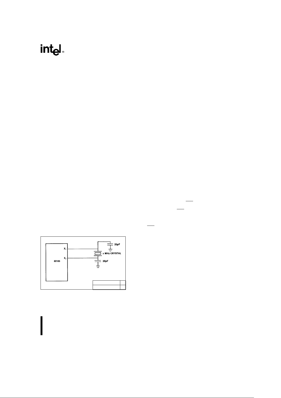
Oscillator
The oscillator circuit is designed to be used with a
parallel resonant fundamental mode crystal. This is
used as the time base for the processor. The crystal
frequency selected will be double the CPU clock frequency. Use of an LC or RC circuit is not recommended with this oscillator. If an external oscillator is
used, it can be connected directly to the input pin X1
in lieu of a crystal. The output of the oscillator is not
directly available outside the processor. The recommended crystal configuration is shown in Figure 5.
x
80186-10 (10 MHz) 20
272430– 5
80186 (8 MHz) 16
Figure 5. Recommended
Crystal Configuration
Intel recommends the following values for crystal selection parameters:
Temperature Range: 0 to 70
§
C
ESR (Equivalent Series Resistance): 30X max
C
0
(Shunt Capacitance of Crystal): 7.0 pf max
C
1
(Load Capacitance): 20 pfg2pf
Drive Level: 1 mW max
Clock Generator
The clock generator provides the 50% duty cycle
processor clock for the processor. It does this by
dividing the oscillator output by 2 forming the symmetrical clock. If an external oscillator is used, the
state of the clock generator will change on the falling edge of the oscillator signal. The CLKOUT pin
provides the processor clock signal for use outside
the device. This may be used to drive other system
components. All timings are referenced to the output
clock.
READY Synchronization
The processor provides both synchronous and asynchronous ready inputs. In addition, the processor, as
part of the integrated chip-select logic, has the capability to program WAIT states for memory and
peripheral blocks.
RESET Logic
The processor provides both a RES input pin and a
synchronized RESET output pin for use with other
system components. The RES
input pin is provided
with hysteresis in order to facilitate power-on Reset
generation via an RC network. RESET output is
guaranteed to remain active for at least five clocks
given a RES input of at least six clocks.
LOCAL BUS CONTROLLER
The processor provides a local bus controller to
generate the local bus control signals. In addition, it
employs a HOLD/HLDA protocol for relinquishing
the local bus to other bus masters. It also provides
outputs that can be used to enable external buffers
and to direct the flow of data on and off the local
bus.
9
9

80186/80188
Memory/Peripheral Control
The processor provides ALE, RD, and WR bus control signals. The RD
and WR signals are used to
strobe data from memory or I/O to the processor or
to strobe data from the processor to memory or I/O.
The ALE line provides a strobe to latch the address
when it is valid. The local bus controller does not
provide a memory/I/O
signal. If this is required, use
the S2
signal (which will require external latching),
make the memory and I/O spaces nonoverlapping,
or use only the integrated chip-select circuitry.
Local Bus Arbitration
The processor uses a HOLD/HLDA system of local
bus exchange. This provides an asynchronous bus
exchange mechanism. This means multiple masters
utilizing the same bus can operate at separate clock
frequencies. The processor provides a single
HOLD/HLDA pair through which all other bus masters may gain control of the local bus. External circuitry must arbitrate which external device will gain
control of the bus when there is more than one alternate local bus master. When the processor relinquishes control of the local bus, it floats DEN
,RD,
WR
,S0–S2, LOCK, AD0– AD15 (AD0–AD7),
A16–A19 (A8 – A19), BHE
(S7), and DT/R to allow
another master to drive these lines directly.
Local Bus Controller and Reset
During RESET the local bus controller will perform
the following action:
#
Drive DEN,RD, and WR HIGH for one clock cycle, then float.
NOTE:
RD
is also provided with an internal pull-up device to prevent the processor from inadvertently
entering Queue Status Mode during RESET.
#
Drive S0–S2 to the inactive state (all HIGH) and
then float.
#
Drive LOCK HIGH and then float.
#
Float AD0 – 15 (AD0 – AD7), A16 – 19 (A8–A19),
BHE
(S7), DT/R.
#
Drive ALE LOW (ALE is never floated).
#
Drive HLDA LOW.
PERIPHERAL ARCHITECTURE
All of the integrated peripherals are controlled by
16-bit registers contained within an internal 256-byte
control block. The control block may be mapped into
either memory or I/O space. Internal logic will recognize control block addresses and respond to bus cycles. During bus cycles to internal registers, the bus
controller will signal the operation externally (i.e., the
RD
,WR, status, address, data, etc., lines will be driv-
en as in a normal bus cycle), but D
15–0(D7–0
),
SRDY, and ARDY will be ignored. The base address
of the control block must be on an even 256-byte
boundary (i.e., the lower 8 bits of the base address
are all zeros).
The control block base address is programmed by a
16-bit relocation register contained within the control
block at offset FEH from the base address of the
control block. It provides the upper 12 bits of the
base address of the control block.
In addition to providing relocation information for the
control block, the relocation register contains bits
which place the interrupt controller into Slave Mode,
and cause the CPU to interrupt upon encountering
ESC instructions.
Chip-Select/Ready Generation Logic
The processor contains logic which provides
programmable chip-select generation for both memories and peripherals. In addition, it can be programmed to provide READY (or WAIT state) generation. It can also provide latched address bits A1 and
A2. The chip-select lines are active for all memory
and I/O cycles in their programmed areas, whether
they be generated by the CPU or by the integrated
DMA unit.
MEMORY CHIP SELECTS
The processor provides 6 memory chip select outputs for 3 address areas; upper memory, lower
memory, and midrange memory. One each is provided for upper memory and lower memory, while four
are provided for midrange memory.
UPPER MEMORY CS
The processor provides a chip select, called UCS,
for the top of memory. The top of memory is usually
used as the system memory because after reset the
processor begins executing at memory location
FFFF0H.
LOWER MEMORY CS
The processor provides a chip select for low memory called LCS
. The bottom of memory contains the
interrupt vector table, starting at location 00000H.
10
10

80186/80188
The lower limit of memory defined by this chip select
is always 0H, while the upper limit is programmable.
By programming the upper limit, the size of the
memory block is defined.
MID-RANGE MEMORY CS
The processor provides four MCS lines which are
active within a user-locatable memory block. This
block can be located within the 1-Mbyte memory address space exclusive of the areas defined by UCS
and LCS. Both the base address and size of this
memory block are programmable.
PERIPHERAL CHIP SELECTS
The processor can generate chip selects for up to
seven peripheral devices. These chip selects are active for seven contiguous blocks of 128 bytes above
a programmable base address. The base address
may be located in either memory or I/O space. Seven CS
lines called PCS0– 6 are generated by the
processor. PCS5
and PCS6 can also be programmed to provide latched address bits A1 and A2.
If so programmed, they cannot be used as peripheral selects. These outputs can be connected directly
to the A0 and A1 pins used for selecting internal
registers of 8-bit peripheral chips.
READY GENERATION LOGIC
The processor can generate a READY signal internally for each of the memory or peripheral CS
lines.
The number of WAIT states to be inserted for each
peripheral or memory is programmable to provide
0–3 wait states for all accesses to the area for
which the chip select is active. In addition, the processor may be programmed to either ignore external
READY for each chip-select range individually or to
factor external READY with the integrated ready
generator.
CHIP SELECT/READY LOGIC AND RESET
Upon RESET, the Chip-Select/Ready Logic will perform the following actions:
#
All chip-select outputs will be driven HIGH.
#
Upon leaving RESET, the UCS line will be programmed to provide chip selects to a 1K block
with the accompanying READY control bits set at
011 to insert 3 wait states in conjunction with external READY (i.e., UMCS resets to FFFBH).
#
No other chip select or READY control registers
have any predefined values after RESET. They
will not become active until the CPU accesses
their control registers. Both the PACS and MPCS
registers must be accessed before the PCS lines
will become active.
DMA Channels
The DMA controller provides two independent DMA
channels. Data transfers can occur between memory and I/O spaces (e.g., Memory to I/O) or within the
same space (e.g., Memory to Memory or I/O to I/O).
Data can be transferred either in bytes or in words
(80186 only) to or from even or odd addresses.
Each DMA channel maintains both a 20-bit source
and destination pointer which can be optionally incremented or decremented after each data transfer
(by one or two depending on byte or word transfers).
Each data transfer consumes 2 bus cycles (a minimum of 8 clocks), one cycle to fetch data and the
other to store data. This provides a maximum data
transfer rate of 1.25 Mword/sec or 2.5 Mbytes/sec
at 10 MHz (half of this rate for the 80188).
DMA CHANNELS AND RESET
Upon RESET, the DMA channels will perform the
following actions:
#
The Start/Stop bit for each channel will be reset
to STOP.
#
Any transfer in progress is aborted.
Timers
The processor provides three internal 16-bit programmable timers. Two of these are highly flexible
and are connected to four external pins (2 per timer).
They can be used to count external events, time external events, generate nonrepetitive waveforms,
etc. The third timer is not connected to any external
pins, and is useful for real-time coding and time delay applications. In addition, the third timer can be
used as a prescaler to the other two, or as a DMA
request source.
11
11

80186/80188
TIMERS AND RESET
Upon RESET, the Timers will perform the following
actions:
#
All EN (Enable) bits are reset preventing timer
counting.
#
For Timers 0 and 1, the RIU bits are reset to zero
and the ALT bits are set to one. This results in the
Timer Out pins going high.
Interrupt Controller
The processor can receive interrupts from a number
of sources, both internal and external. The internal
interrupt controller serves to merge these requests
on a priority basis, for individual service by the CPU.
Internal interrupt sources (Timers and DMA channels) can be disabled by their own control registers
or by mask bits within the interrupt controller. The
interrupt controller has its own control register that
sets the mode of operation for the controller.
INTERRUPT CONTROLLER AND RESET
Upon RESET, the interrupt controller will perform
the following actions:
#
All SFNM bits reset to 0, implying Fully Nested
Mode.
#
All PR bits in the various control registers set to 1.
This places all sources at lowest priority (level
111).
#
All LTM bits reset to 0, resulting in edge-sense
mode.
#
All Interrupt Service bits reset to 0.
#
All Interrupt Request bits reset to 0.
#
All MSK (Interrupt Mask) bits set to 1 (mask).
#
All C (Cascade) bits reset to 0 (non-Cascade).
#
All PRM (Priority Mask) bits set to 1, implying no
levels masked.
#
Initialized to Master Mode.
12
12

80186/80188
272430– 6
NOTE:
Pin names in parenthesis apply to 80188.
(1) BHE
does not exist on the 80188, this is only required for a 16-bit data bus.
Figure 6. Typical 80186/80188 Computer
13
13

80186/80188
272430– 7
NOTE:
Pin names in parentheses apply to 80188.
(1) BHE does not exist on the 80188, this is only required for a 16-bit data bus.
Figure 7. Typical 80186/80188 Multi-Master Bus Interface
14
14

80186/80188
ABSOLUTE MAXIMUM RATINGS*
Ambient Temperature under Bias АААААА0§Cto70§C
Storage Temperature ААААААААААb65§Ctoa150§C
Voltage on any Pin with
Respect to GroundАААААААААААААА
b
1.0V toa7V
Power Dissipation ААААААААААААААААААААААААААА3W
NOTICE: This is a production data sheet. The specifications are subject to change without notice.
*
WARNING: Stressing the device beyond the ‘‘Absolute
Maximum Ratings’’ may cause permanent damage.
These are stress ratings only. Operation beyond the
‘‘Operating Conditions’’ is not recommended and extended exposure beyond the ‘‘Operating Conditions’’
may affect device reliability.
D.C. CHARACTERISTICS (T
A
e
0§Ctoa70§C, V
CC
e
5Vg10%)
Applicable to 8 MHz and 10 MHz devices.
Symbol Parameter Min Max Units Test Conditions
V
IL
Input Low Voltage
b
0.5
a
0.8 V
V
IH
Input High Voltage 2.0 V
CC
a
0.5 V
(All except X1 and (RES
)
V
IH1
Input High Voltage (RES) 3.0 V
CC
a
0.5 V
V
OL
Output Low Voltage 0.45 V I
a
e
2.5 mA for S0 –S2
I
a
e
2.0 mA for all other Outputs
V
OH
Output High Voltage 2.4 V I
oa
eb
400 mA
I
CC
Power Supply Current 600* mA T
A
eb
40§C
550 mA T
A
e
0§C
415 mA T
A
ea
70§C
I
LI
Input Leakage Current
g
10 mA0V
k
V
IN
k
V
CC
I
LO
Output Leakage Current
g
10 mA 0.45VkV
OUT
k
V
CC
V
CLO
Clock Output Low 0.6 V I
a
e
4.0 mA
V
CHO
Clock Output High 4.0 V I
oa
eb
200 mA
V
CLI
Clock Input Low Voltage
b
0.5 0.6 V
V
CHI
Clock Input High Voltage 3.9 V
CC
a
1.0 V
C
IN
Input Capacitance 10 pF
C
IO
I/O Capacitance 20 pF
*For extended temperature parts only.
15
15

80186/80188
A.C. CHARACTERISTICS (T
A
e
0§Ctoa70§C, V
CC
e
5Vg10%)
Timing Requirements All Timings Measured At 1.5V Unless Otherwise Noted.
Symbol Parameter
8 MHz 10 MHz
Units
Conditions
Test
Min Max Min Max
T
DVCL
Data in Setup (A/D) 20 15 ns
T
CLDX
Data in Hold (A/D) 10 8 ns
T
ARYHCH
Asynchronous Ready 20 15 ns
(ARDY) Active Setup
Time
(1)
T
ARYLCL
ARDY Inactive Setup Time 35 25 ns
T
CLARX
ARDY Hold Time 15 15 ns
T
ARYCHL
Asynchronous Ready 15 15 ns
Inactive Hold Time
T
SRYCL
Synchronous Ready (SRDY) 20 20 ns
Transition Setup Time
(2)
T
CLSRY
SRDY Transition Hold 15 15 ns
Time
(2)
T
HVCL
HOLD Setup
(1)
25 20 ns
T
INVCH
INTR, NMI, TEST, TIM IN, 25 25 ns
Setup
(1)
T
INVCL
DRQ0, DRQ1, Setup
(1)
25 20 ns
Master Interface Timing Responses
T
CLAV
Address Valid Delay 5 55 5 44 ns C
L
e
20 pF–200 pF
all Outputs
T
CLAX
Address Hold 10 10 ns
(Except T
CLTMV
)
@
8 MHz and 10 MHz
T
CLAZ
Address Float Delay T
CLAX
35 T
CLAX
30 ns
T
CHCZ
Command Lines Float Delay 45 40 ns
T
CHCV
Command Lines Valid Delay 55 45 ns
(after Float)
T
LHLL
ALE Width T
CLCL
b
35 T
CLCL
b
30 ns
T
CHLH
ALE Active Delay 35 30 ns
T
CHLL
ALE Inactive Delay 35 30 ns
T
LLAX
Address Hold from ALE T
CHCL
b
25 T
CHCL
b
20 ns
Inactive
T
CLDV
Data Valid Delay 10 44 10 40 ns
T
CLDOX
Data Hold Time 10 10 ns
T
WHDX
Data Hold after WR T
CLCL
b
40 T
CLCL
b
34 ns
T
CVCTV
Control Active Delay 1 5 50 5 40 ns
T
CHCTV
Control Active Delay 2 10 55 10 44 ns
T
CVCTX
Control Inactive Delay 5 55 5 44 ns
T
CVDEX
DEN Inactive Delay 10 70 10 56 ns
(Non-Write Cycle)
1. To guarantee recognition at next clock.
2. To guarantee proper operation.
16
16

80186/80188
A.C. CHARACTERISTICS (T
A
e
0§Ctoa70§C, V
CC
e
5Vg10%) (Continued)
Master Interface Timing Responses (Continued)
Symbol Parameter
8 MHz 10 MHz
Units
Conditions
Test
Min Max Min Max
T
AZRL
Address Float to RD Active 0 0 ns
T
CLRL
RD Active Delay 10 70 10 56 ns
T
CLRH
RD Inactive Delay 10 55 10 44 ns
T
RHAV
RD Inactive to Address T
CLCL
b
40 T
CLCL
b
40 ns
Active
T
CLHAV
HLDA Valid Delay 5 50 5 40 ns
T
RLRH
RD Width 2T
CLCL
b
50 2T
CLCL
b
46 ns
T
WLWH
WR Width 2T
CLCL
b
40 2T
CLCL
b
34 ns
T
AVLL
Address Valid to ALE Low T
CLCH
b
25 T
CLCH
b
19 ns
T
CHSV
Status Active Delay 10 55 10 45 ns
T
CLSH
Status Inactive Delay 10 65 10 50 ns
T
CLTMV
Timer Output Delay 60 48 ns 100 pF max
@
8&10MHz
T
CLRO
Reset Delay 60 48 ns
T
CHQSV
Queue Status Delay 35 28 ns
T
CHDX
Status Hold Time 10 10 ns
T
AVCH
Address Valid to Clock High 10 10 ns
T
CLLV
LOCK Valid/Invalid Delay 5 65 5 60 ns
Chip-Select Timing Responses
T
CLCSV
Chip-Select Active Delay 66 45 ns
T
CXCSX
Chip-Select Hold from 35 35 ns
Command Inactive
T
CHCSX
Chip-Select Inactive Delay 5 35 5 32 ns
CLKIN Requirements
T
CKIN
CLKIN Period 62.5 250 50 250 ns
T
CKHL
CLKIN Fall Time 10 10 ns 3.5 to 1.0V
T
CKLH
CLKIN Rise Time 10 10 ns 1.0 to 3.5V
T
CLCK
CLKIN Low Time 25 20 ns 1.5V
T
CHCK
CLKIN High Time 25 20 ns 1.5V
CLKOUT Timing (200 pF load)
T
CICO
CLKIN to CLKOUT Skew 50 25 ns
T
CLCL
CLKOUT Period 125 500 100 500 ns
T
CLCH
CLKOUT Low Time (/2 T
CLCL
b
7.5 (/2 T
CLCL
b
6.0 ns 1.5V
T
CHCL
CLKOUT High Time (/2 T
CLCL
b
7.5 (/2 T
CLCL
b
6.0 ns 1.5V
T
CH1CH2
CLKOUT Rise Time 15 12 ns 1.0 to 3.5V
T
CL2CL1
CLKOUT Fall Time 15 12 ns 3.5 to 1.0V
17
17

80186/80188
EXPLANATION OF THE AC SYMBOLS
Each timing symbol has from 5 to 7 characters. The
first character is always a ‘‘T’’ (stands for time). The
other characters, depending on their positions,
stand for the name of a signal or the logical status of
that signal. The following is a list of all the characters and what they stand for.
A: Address
ARY: Asynchronous Ready Input
C: Clock Output
CK: Clock Input
CS: Chip Select
CT: Control (DT/R
, DEN,...)
D: Data Input
DE: DEN
H: Logic Level High
IN: Input (DRQ0, TIM0, . . . )
L: Logic Level Low or ALE
O: Output
QS: Queue Status (QS1, QS2)
R: RD
signal, RESET signal
S: Status (S0
,S1,S2)
SRY: Synchronous Ready Input
V: Valid
W: WR Signal
X: No Longer a Valid Logic Level
Z: Float
Examples:
T
CLAV
Ð Time from Clock low to Address valid
T
CHLH
Ð Time from Clock high to ALE high
T
CLCSV
Ð Time from Clock low to Chip Select valid
18
18

80186/80188
WAVEFORMS
MAJOR CYCLE TIMING
272430– 8
NOTE:
Pin names in parentheses apply to the 80188.
19
19

80186/80188
WAVEFORMS (Continued)
MAJOR CYCLE TIMING (Continued)
NOTES: 272430– 9
1. INTA occurs one clock later in slave mode.
2. Status inactive just prior to T
4
.
3. If latched A1 and A2 are selected instead of PCS5
and PCS6, only T
CLCSV
is applicable.
4. Pin names in parentheses apply to the 80188.
20
20

80186/80188
WAVEFORMS (Continued)
272430– 10
272430– 11
272430– 12
21
21

80186/80188
WAVEFORMS (Continued)
272430– 13
272430– 14
22
22

80186/80188
WAVEFORMS (Continued)
READY TIMING
272430– 15
23
23

80186/80188
272430– 16
NOTE:
Pin names in parentheses apply to the 80188.
24
24

80186/80188
WAVEFORMS (Continued)
272430– 17
EXPRESS
The Intel EXPRESS system offers enhancements to
the operational specifications of the microprocessor.
EXPRESS products are designed to meet the needs
of those applications whose operating requirements
exceed commercial standards.
The EXPRESS program includes the commercial
standard temperature range with burn-in and an extended temperature range without burn-in.
With the commercial standard temperature range
operational characteristics are guaranteed over the
temperature range of 0
§
Ctoa70§C. With the extended temperature range option, operational characteristics are guaranteed over the range of
b
40§C
to
a
85§C.
The optional burn-in is dynamic, for a minimum time
of 160 hours at
a
125§C with V
CC
e
5.5Vg0.25V,
following guidelines in MIL-STD-883, Method 1015.
Package types and EXPRESS versions are identified
by a one- or two-letter prefix to the part number. The
prefixes are listed in Table 2. All A.C. and D.C. specifications not mentioned in this section are the same
for both commercial and EXPRESS parts.
Table 2. Prefix Identification
Prefix
Package Temperature
Burn-In
Type Range
A PGA Commercial No
N PLCC Commercial No
R LCC Commercial No
TA PGA Extended No
QA PGA Commercial Yes
QR LCC Commercial Yes
NOTE:
Not all package/temperature range/speed combinations
are available.
25
25

80186/80188
EXECUTION TIMINGS
A determination of program execution timing must
consider the bus cycles necessary to prefetch instructions as well as the number of execution unit
cycles necessary to execute instructions. The following instruction timings represent the minimum execution time in clock cycles for each instruction. The
timings given are based on the following assumptions:
#
The opcode, along with any data or displacement
required for execution of a particular instruction,
has been prefetched and resides in the queue at
the time it is needed.
#
No wait states or bus HOLDS occur.
#
All word-data is located on even-address boundaries.
All instructions which involve memory accesses can
also require one or two additional clocks above the
minimum timings shown due to the asynchronous
handshake between the bus interface unit (BIU) and
execution unit.
All jumps and calls include the time required to fetch
the opcode of the next instruction at the destination
address.
The 80186 has sufficient bus performance to ensure
that an adequate number of prefetched bytes will
reside in the queue (6 bytes) most of the time.
Therefore, actual program execution time will not be
substantially greater than that derived from adding
the instruction timings shown.
The 80188 is noticeably limited in its performance
relative to the execution unit. A sufficient number of
prefetched bytes may not reside in the prefetch
queue (4 bytes) much of the time. Therefore, actual
program execution time may be substantially greater
than that derived from adding the instruction timings
shown.
26
26

80186/80188
INSTRUCTION SET SUMMARY
80186 80188
Function Format Clock Clock Comments
Cycles Cycles
DATA TRANSFER
MOV
e
Move:
Register to Register/Memory 1000100w modreg r/m 2/12 2/12*
Register/memory to register 1000101w modreg r/m 2/9 2/9*
Immediate to register/memory 1100011w mod000 r/m data data if we1 12/13 12/13 8/16-bit
Immediate to register 1011w reg data data if we1 3/4 3/4 8/16-bit
Memory to accumulator 1010000w addr-low addr-high 8 8*
Accumulator to memory 1010001w addr-low addr-high 9 9*
Register/memory to segment register 10001110 mod0reg r/m 2/9 2/13
Segment register to register/memory 10001100 mod0reg r/m 2/11 2/15
PUSHePush:
Memory 11111111 mod110 r/m 16 20
Register 01010 reg 10 14
Segment register 000reg110 9 13
Immediate 011010s0 data data if se01014
PUSHAePush All 01100000 36 68
POPePop:
Memory 10001111 mod000 r/m 20 24
Register 01011 reg 10 14
Segment register 000reg111 (regi01) 8 12
POPAePopAll 01100001 51 83
XCHGeExchange:
Register/memory with register 1000011w modreg r/m 4/17 4/17*
Register with accumulator 10010 reg 3 3
INeInput from:
Fixed port 1110010w port 10 10*
Variable port 1110110w 8 8*
OUTeOutput to:
Fixed port 1110011w port 9 9*
Variable port 1110111w 7 7*
XLATeTranslate byte to AL 11010111 11 15
LEAeLoad EA to register 10001101 modreg r/m 6 6
LDSeLoad pointer to DS 11000101 modreg r/m (modi11) 18 26
LESeLoad pointer to ES 11000100 modreg r/m (modi11) 18 26
LAHFeLoad AH with flags 10011111 2 2
SAHFeStore AH into flags 10011110 3 3
PUSHFePush flags 10011100 9 13
POPFePop flags 10011101 8 12
Shaded areas indicate instructions not available in 8086, 8088 microsystems.
NOTE:
*Clock cycles shown for byte transfers, for word operations, add 4 clock cycles for each memory transfer.
27
27

80186/80188
INSTRUCTION SET SUMMARY (Continued)
80186 80188
Function Format Clock Clock Comments
Cycles Cycles
DATA TRANSFER (Continued)
SEGMENT
e
Segment Override:
CS 00101110 2 2
SS 00110110 2 2
DS 00111110 2 2
ES 00100110 2 2
ARITHMETIC
ADD
e
Add:
Reg/memory with register to either 000000dw modreg r/m 3/10 3/10*
Immediate to register/memory 100000sw mod000 r/m data data if s we01 4/16 4/16*
Immediate to accumulator 0000010w data data if we1 3/4 3/4 8/16-bit
ADCeAdd with carry:
Reg/memory with register to either 000100dw modreg r/m 3/10 3/10*
Immediate to register/memory 100000sw mod010 r/m data data if s we01 4/16 4/16*
Immediate to accumulator 0001010w data data if we1 3/4 3/4 8/16-bit
INCeIncrement:
Register/memory 1111111w mod000 r/m 3/15 3/15*
Register 01000 reg 3 3
SUBeSubtract:
Reg/memory and register to either 001010dw modreg r/m 3/10 3/10*
Immediate from register/memory 100000sw mod101 r/m data data if s we01 4/16 4/16*
Immediate from accumulator 0010110w data data if we1 3/4 3/4 8/16-bit
SBBeSubtract with borrow:
Reg/memory and register to either 000110dw modreg r/m 3/10 3/10*
Immediate from register/memory 100000sw mod011 r/m data data if s we01 4/16 4/16*
Immediate from accumulator 0001110w data data if we1 3/4 3/4 8/16-bit
DECeDecrement
Register/memory 1111111w mod001 r/m 3/15 3/15*
Register 01001 reg 3 3
CMPeCompare:
Register/memory with register 0011101w modreg r/m 3/10 3/10*
Register with register/memory 0011100w modreg r/m 3/10 3/10*
Immediate with register/memory 100000sw mod111 r/m data data if s we01 3/10 3/10*
Immediate with accumulator 0011110w data data if we1 3/4 3/4 8/16-bit
NEGeChange sign register/memory 1111011w mod011 r/m 3/10 3/10*
AAAeASCII adjust for add 00110111 8 8
DAAeDecimal adjust for add 00100111 4 4
AASeASCII adjust for subtract 00111111 7 7
DASeDecimal adjust for subtract 00101111 4 4
MULeMultiply (unsigned): 1111011w mod100 r/m
Register-Byte 26–28 26–28
Register-Word 35–37 35–37
Memory-Byte 32–34 32–34
Memory-Word 41–43 41–43*
Shaded areas indicate instructions not available in 8086, 8088 microsystems.
NOTE:
*Clock cycles shown for byte transfers, for word operations, add 4 clock cycles for each memory transfer.
28
28

80186/80188
INSTRUCTION SET SUMMARY (Continued)
80186 80188
Function Format Clock Clock Comments
Cycles Cycles
ARITHMETIC (Continued)
IMULeInteger multiply (signed): 1111011w mod101 r/m
Register-Byte 25–28 25–28
Register-Word 34–37 34–37
Memory-Byte 31–34 31–34
Memory-Word 40–43 40–43*
IMULeInteger Immediate multiply 011010s1 modreg r/m data data if se0 22– 25/ 22– 25/
(signed)
29–32 29–32
DIVeDivide (unsigned): 1111011w mod110 r/m
Register-Byte 29 29
Register-Word 38 38
Memory-Byte 35 35
Memory-Word 44 44*
IDIVeInteger divide (signed): 1111011w mod111 r/m
Register-Byte 44–52 44–52
Register-Word 53–61 53–61
Memory-Byte 50–58 50–58
Memory-Word 59–67 59–67*
AAMeASCII adjust for multiply 11010100 00001010 19 19
AADeASCII adjust for divide 11010101 00001010 15 15
CBWeConvert byte to word 10011000 2 2
CWDeConvert word to double word 10011001 4 4
LOGIC
Shift/Rotate Instructions:
Register/Memory by 1 1101000w modTTTr/m 2/15 2/15
Register/Memory by CL 1101001w modTTTr/m
5an/17an5an/17an
Register/Memory by Count 1100000w modTTTr/m count
5an/17an5an/17an
TTT Instruction
000 ROL
001 ROR
010 RCL
011 RCR
1 0 0 SHL/SAL
101 SHR
111 SAR
AND
e
And:
Reg/memory and register to either 001000dw modreg r/m 3/10 3/10*
Immediate to register/memory 1000000w mod100 r/m data data if we1 4/16 4/16*
Immediate to accumulator 0010010w data data if we1 3/4 3/4 8/16-bit
TESTeAnd function to flags, no result:
Register/memory and register 1000010w modreg r/m 3/10 3/10*
Immediate data and register/memory 1111011w mod000 r/m data data if we1 4/10 4/10*
Immediate data and accumulator 1010100w data data if we1 3/4 3/4 8/16-bit
OReOr:
Reg/memory and register to either 000010dw modreg r/m 3/10 3/10*
Immediate to register/memory 1000000w mod001 r/m data data if we1 4/16 4/16*
Immediate to accumulator 0000110w data data if we1 3/4 3/4 8/16-bit
Shaded areas indicate instructions not available in 8086, 8088 microsystems.
NOTE:
*Clock cycles shown for byte transfers, for word operations, add 4 clock cycles for each memory transfer.
29
29

80186/80188
INSTRUCTION SET SUMMARY (Continued)
80186 80188
Function Format Clock Clock Comments
Cycles Cycles
LOGIC (Continued)
XOR
e
Exclusive or:
Reg/memory and register to either 001100dw modreg r/m 3/10 3/10*
Immediate to register/memory 1000000w mod110 r/m data data if we1 4/16 4/16*
Immediate to accumulator 0011010w data data if we1 3/4 3/4 8/16-bit
NOTeInvert register/memory 1111011w mod010 r/m 3/10 3/10*
STRING MANIPULATION
MOVSeMove byte/word 1010010w 14 14*
CMPSeCompare byte/word 1010011w 22 22*
SCASeScan byte/word 1010111w 15 15*
LODSeLoad byte/wd to AL/AX 1010110w 12 12*
STOSeStore byte/wd from AL/AX 1010101w 10 10*
INSeInput byte/wd from DX port 0110110w 14 14
OUTSeOutput byte/wd to DX port 0110111w 14 14
Repeated by count in CX (REP/REPE/REPZ/REPNE/REPNZ)
MOVSeMove string 11110010 1010010w 8a8n 8a8n*
CMPSeCompare string 1111001z 1010011w 5a22n 5a22n*
SCASeScan string 1111001z 1010111w 5a15n 5a15n*
LODSeLoad string 11110010 1010110w 6a11n 6a11n*
STOSeStore string 11110010 1010101w 6a9n 6a9n*
INSeInput string 11110010 0110110w 8a8n 8a8n*
OUTSeOutput string 11110010 0110111w 8a8n 8a8n*
CONTROL TRANSFER
CALL
e
Call:
Direct within segment 11101000 disp-low disp-high 15 19
Register/memory 11111111 mod010 r/m 13/19 17/27
indirect within segment
Direct intersegment 10011010 segment offset 23 31
segment selector
Indirect intersegment 11111111 mod011 r/m (modi11) 38 54
JMPeUnconditional jump:
Short/long 11101011 disp-low 14 14
Direct within segment 11101001 disp-low disp-high 14 14
Register/memory 11111111 mod100 r/m 11/17 11/21
indirect within segment
Direct intersegment 11101010 segment offset 14 14
segment selector
Indirect intersegment 11111111 mod101 r/m (modi11) 26 34
Shaded areas indicate instructions not available in 8086, 8088 microsystems.
NOTE:
*Clock cycles shown for byte transfers, for word operations, add 4 clock cycles for each memory transfer.
30
30

80186/80188
INSTRUCTION SET SUMMARY (Continued)
80186 80188
Function Format Clock Clock Comments
Cycles Cycles
CONTROL TRANSFER (Continued)
RET
e
Return from CALL:
Within segment 11000011 16 20
Within seg adding immed to SP 11000010 data-low data-high 18 22
Intersegment 11001011 22 30
Intersegment adding immediate to SP 11001010 data-low data-high 25 33
JE/JZeJump on equal/zero 01110100 disp 4/13 4/13 JMP not
JL/JNGEeJump on less/not greater or equal 01111100 disp 4/13 4/13
taken/JMP
JLE/JNGeJump on less or equal/not greater 01111110 disp 4/13 4/13
taken
JB/JNAEeJump on below/not above or equal 01110010 disp 4/13 4/13
JBE/JNAeJump on below or equal/not above 01110110 disp 4/13 4/13
JP/JPEeJump on parity/parity even 01111010 disp 4/13 4/13
JOeJump on overflow 01110 000 disp 4/13 4/13
JSeJump on sign 01111000 disp 4/13 4/13
JNE/JNZeJump on not equal/not zero 01110101 disp 4/13 4/13
JNL/JGEeJump on not less/greater or equal 01111101 disp 4/13 4/13
JNLE/JGeJump on not less or equal/greater 01111111 disp 4/13 4/13
JNB/JAEeJump on not below/above or equal 01110011 disp 4/13 4/13
JNBE/JAeJump on not below or equal/above 01110111 disp 4/13 4/13
JNP/JPOeJump on not par/par odd 01111011 disp 4/13 4/13
JNOeJump on not overflow 01110001 disp 4/13 4/13
JNSeJump on not sign 01111001 disp 4/13 4/13
JCXZeJump on CX zero 11100011 disp 5/15 5/15
LOOPeLoop CX times 11100010 disp 6/16 6/16 LOOP not
LOOPZ/LOOPEeLoop while zero/equal 11100001 disp 6/16 6/16
taken/LOOP
LOOPNZ/LOOPNEeLoop while not zero/equal 11100000 disp 6/16 6/16
taken
ENTEReEnter Procedure 11001000 data-low data-high L
Le0 15 19
L
e
1 25 29
L
l
1
22a16(nb1) 26a20(nb1)
LEAVEeLeave Procedure 11001001 8 8
INTeInterrupt:
Type specified 11001101 type 47 47
Type 3 11001100 45 45 ifINT. taken/
INTOeInterrupt on overflow 11001110 48/4 48/4
if INT. not
taken
IRETeInterrupt return 11001111 28 28
BOUNDeDetect value out of range 01100010 modreg r/m 33–35 33–35
Shaded areas indicate instructions not available in 8086, 8088 microsystems.
NOTE:
*Clock cycles shown for byte transfers, for word operations, add 4 clock cycles for each memory transfer.
31
31

80186/80188
INSTRUCTION SET SUMMARY (Continued)
80186 80188
Function Format Clock Clock Comments
Cycles Cycles
PROCESSOR CONTROL
CLCeClear carry 11111000 2 2
CMCeComplement carry 11110101 2 2
STCeSet carry 11111001 2 2
CLDeClear direction 11111100 2 2
STDeSet direction 11111101 2 2
CLIeClear interrupt 11111010 2 2
STIeSet interrupt 11111011 2 2
HLTeHalt 11110100 2 2
WAITeWait 10011011 6 6 ifTESTe0
LOCKeBus lock prefix 11110000 2 3
ESCeProcessor Extension Escape 11011TTT modLLL r/m 6 6
(TTT LLL are opcode to processor extension)
NOPeNo Operation 10010000 3 3
Shaded areas indicate instructions not available in 8086, 8088 microsystems.
NOTE:
*Clock cycles shown for byte transfers, for word operations, add 4 clock cycles for each memory transfer.
FOOTNOTES
The Effective Address (EA) of the memory operand
is computed according to the mod and r/m fields:
if mode11 then r/m is treated as REG field
if mod
e
00 then DISPe0*, disp-low and disp-high are absent
if mod
e
01 then DISPedisp-low sign-extended to 16-bits, disp-high
is absent
if mod
e
10 then DISPedisp-high: disp-low
if r/m
e
000 then EAe(BX)a(SI)aDISP
if r/m
e
001 then EAe(BX)a(DI)aDISP
if r/m
e
010 then EAe(BP)a(SI)aDISP
if r/m
e
011 then EAe(BP)a(DI)aDISP
if r/m
e
100 then EAe(SI)aDISP
if r/m
e
101 then EAe(DI)aDISP
if r/m
e
110 then EAe(BP)aDISP*
if r/m
e
111 then EAe(BX)aDISP
DISP follows 2nd byte of instruction (before data if
required)
*except if mod
e
00 and r/me110 then EA
e
disp-high: disp-low.
EA calculation time is 4 clock cycles for all modes,
and is included in the execution times given whenever appropriate.
Segment Override Prefix
0 0 1 reg 1 1 0
reg is assigned according to the following:
reg
Segment
Register
00 ES
01 CS
10 SS
11 DS
REG is assigned according to the following table:
16-Bit (w
e
1) 8-Bit (we0)
000 AX 000 AL
001 CX 001 CL
010 DX 010 DL
011 BX 011 BL
100 SP 100 AH
101 BP 101 CH
110 SI 110 DH
111 DI 111 BH
The physical addresses of all operands addressed
by the BP register are computed using the SS segment register. The physical addresses of the destination operands of the string primitive operations
(those addressed by the DI register) are computed
using the ES segment, which may not be overridden.
32
32

80186/80188
REVISION HISTORY
This data sheet replaces the following data sheets:
210706-011 80188
210451-011 80186
33
33
 Loading...