

Intel Corporation PA28F016S5-120 Datasheet

E
SMART 5 FlashFile™ MEMORY FAMILY
4, 8, AND 16 MBIT
28F004S5, 28F008S5, 28F016S5
Includes Commercial and Extended Temperature Specifications
n
SmartVoltage Technology
Smart 5 Flash: 5V VCC and 5V or
12V V
PP
n
High-Performance
4, 8 Mbit: 85 ns Read Access Time
16 Mbit: 95 ns Read Access Time
n
Enhanced Data Protection Features
Absolute Protection with VPP = GND
Flexible Block Locking
Block Write Lockout during Power
Transitions
n
Enhanced Automated Suspend Options
Program Suspend to Read
Block Erase Suspend to Program
Block Erase Suspend to Read
n
Industry-Standard Packaging
40-Lead TSOP, 44-Lead PSOP
BYTE-WIDE
n
High-Density 64-Kbyte Symmetrical
Erase Block Architecture
n
Extended Cycling Capability
n
Low Power Management
n
Automated Program and Block Erase
n
SRAM-Compatible Write Interface
n
ETOX™ V Nonvolatile Flash
Technology
PRODUCT PREVIEW
4 Mbit: Eight Blocks
8 Mbit: Sixteen Blocks
16 Mbit: Thirty-Two Blocks
100,000 Block Erase Cycles
Deep Power-Down Mode
Automatic Power Savings Mode
Decreases I
Command User Interface
Status Register
in Static Mode
CC
Intel’s byte-wide Smart 5 FlashFile™ memory family renders a variety of density offerings in the same
package. The 4-, 8-, and 16-Mbit byte-wide FlashFile memories provide high-density, low-cost, nonv olatile,
read/write storage solutions for a wide range of applications. Their symmetricall y-blocked architect ure, flexible
voltage, and extended cy cling provide highly flexible components suitable for resident flash arrays , SIMMs,
and memory cards. Enhanced suspend capabilities provide an ideal solution for code or data storage
applications. For secure code storage applications, such as networking, where code is either directly
executed out of flash or downl oaded to DRAM, the 4-, 8-, and 16-Mbit FlashFile mem ories offer three lev els
of protection: absolute protection with V
block locking. These alternatives give designers ultimate control of their code security needs.
This family of products is manufactured on Intel’s 0.4 µm ETOX™ V process technology. They come in
industry-standard packages: the 40-lead TSOP, ideal for board-constrained applications, and the rugged
44-lead PSOP. Based on the 28F008SA architecture, the byte-wide Smart 5 FlashFile memory family
enables quick and easy upgrades for designs that demand state-of-the-art technology.
June 1997 Order Number: 290597-003
at GND, selective hardware block locking, or flexible software
PP

Information in this document is provided in connection with Intel products. No license, express or implied, by estoppel or
y
otherwise, to any intellectual property rights is granted by this document. Except as provided in Intel’s Terms and Conditi ons of
Sale for such products, Intel assumes no liability whatsoever, and Intel disclaims any express or implied warranty, relating to
sale and/or use of Intel products including liability or warranties relating to fitness for a particular purpose, merchantability, or
infringement of any patent, copyright or other intellectual property right. Intel products are not intended for use in medical, life
saving, or life sustaining applications.
Intel may make changes to specifications and product descriptions at any time, without notice.
The 28F004S5, 28F008S5, 28F016S 5 may contain design defects or errors known as errata which may cause the product to
deviate from published specifications. Current characterized errata are available on request.
Contact your local Intel sales office or your distributor to obtain the latest specifications and before placing your product order.
Copies of documents which have an ordering number and are referenced in this document, or other Intel literature, may be
obtained from:
Intel Corporation
P.O. Box 7641
Mt. Prospect, IL 60056-7641
or call 1-800-879-4683
or visit Intel’s Website at http:\\www.intel.com
COPYRIGHT © INTEL CORPORATION, 1997 CG-041493
*Third-part
brands and names are the property of their respective owners

E BYTE-WIDE SMART 5 FlashFile™ MEMORY FAMILY
CONTENTS
PAGE PAGE
1.0 INTRODUCTION .............................................5
1.1 New Features...............................................5
1.2 Product Overview.........................................5
1.3 Pinout and Pin Description...........................6
2.0 PRINCIPLES OF OPERATION .......................9
2.1 Data Protection ..........................................10
3.0 BUS OPERATION.........................................10
3.1 Read..........................................................10
3.2 Output Disable...........................................10
3.3 Standby......................................................10
3.4 Deep Power-Down.....................................10
3.5 Read Identifier Codes Operation................11
3.6 Write ..........................................................11
4.0 COMMAND DEFINITIONS............................11
4.1 Read Array Command................................14
4.2 Read Identifier Codes Command...............14
4.3 Read Status Register Command................14
4.4 Clear Status Register Command................14
4.5 Block Erase Command ..............................14
4.6 Program Command....................................15
4.7 Block Erase Suspend Command................15
4.8 Program Suspend Command.....................16
4.9 Set Block and Master Lock-Bit Commands 16
4.10 Clear Block Lock-Bits Command..............17
6.0 ELECTRICAL SPECIFICATIONS..................26
6.1 Absolute Maximum Ratings........................26
6.2 Commercial Temperature Operating
Conditions.................................................26
6.2.1 Capacitance.........................................26
6.2.2 AC Input/Output Test Conditions .........27
6.2.3 Commercial Temperature
DC Characteristics..............................28
6.2.4 Commercial Temperature
AC Characteristics - Read-Only
Operations..........................................30
6.2.5 Commercial Temperature Reset
Operations..........................................31
6.2.6 Commercial Temperature
AC Characteristics - Write Operations32
6.2.7 Commercial Temperature Block Erase,
Program, and Lock-Bit Configuration
Performance.......................................34
6.3 Extended Temperature Operating
Conditions.................................................35
6.3.1 Extended Temperature
DC Characteristics..............................35
6.3.2 Extended Temperature
AC Characteristics - Read-Only
Operations..........................................35
APPENDIX A. Ordering Information..........36
APPENDIX B. Additional Information........37
5.0 DESIGN CONSIDERATIONS........................25
5.1 Three-Line Output Control..........................25
5.2 RY/BY# Hardware Detection......................25
5.3 Power Supply Decoupling..........................25
Trace on Printed Circuit Boards...........25
5.4 V
PP
, VPP, RP# Transitions .........................25
5.5 V
CC
5.6 Power-Up/Down Protection........................25
PRODUCT PREVIEW
3

BYTE-WIDE SMART 5 FlashFile™ MEMORY FAMILY E
REVISION HISTORY
Number Description
-001 Original version
-002 Table 3 revised to reflect change in abbreviations from “W” for write to “P” for program.
-003 Updated disclaimer
Ordering information graphic (Appendix A) corrected: from PB = Ext. Temp. 44-Lead
PSOP to TB = Ext. Temp. 44-Lead PSOP
Updated Ordering Information and table
Correction to table, Section 6.2.3. Under I
or GND, corrected to V
Section 6.2.7, modified Program and Block Erase Suspend Latency Times
= VCC or GND
OUT
Test Conditions, previously read VIN = V
LO
CC
4
PRODUCT PREVIEW

E BYTE-WIDE SMART 5 FlashFile™ MEMORY FAMILY
1.0 INTRODUCTION
This datasheet contains 4-, 8-, and 16-M bit Smart 5
FlashFile memory specifications. Section 1
provides a flash memory ov ervi ew. S ect ions 2, 3, 4,
and 5 describe the memory organization and
functionality. Section 6 covers electrical
specifications for commercial and extended
temperature product offerings. The by te-wide Sm art
5 FlashFile memory family documentation also
includes application notes and design tools which
are referenced in Appendix B.
1.1 New Features
The byte-wide Smart 5 FlashFile memory family
maintains backwards-compatibility with Intel’s
28F008SA. Key enhancements include:
• SmartVoltage Technology
• Enhanced Suspend Capabilities
• In-System Block Locking
They share a compatible status register, software
commands, and pinouts. These similarities enable
a clean upgrade from the 28F008SA to byte-wide
Smart 5 FlashFile products. When upgrading, it is
important to note the following differences:
• Because of new feature and density options,
the devices have different device identifier
codes. This allows for software optimization.
• V
• To take advantage of SmartVoltage tech-
For more details see application note
28F008SC Compatibility with 28F008SA
number 292180)
has been lowered from 6.5V to 1.5V to
PPLK
support low V
program, and lock-bit configuration operations.
Designs that switch V
operations should transition V
nology, allow V
voltages during block erase,
PP
off during read
PP
to GND.
PP
connection to 5V.
PP
.
AP-625,
(order
1.2 Product Overview
The byte-wide Smart 5 FlashFile memory family
provides density upgrades with pinout compatibility
for the 4-, 8-, and 16-Mbit densities. The 28F004S5,
28F008S5, and 28F016S5 are high-performance
memories arranged as 512 Kbyte, 1 Mbyte, and
2 Mbyte of 8 bits. This data is grouped in eight,
sixteen, and thirty-two 64-Kbyte blocks which are
individually erasable, lockable, and unlockable insystem. Figure 4 illustrates the memory
organization.
SmartVoltage technology enables fast factory
programming and low power designs. Specifically
designed for 5V systems, Smart 5 FlashFile
components support read operations at 5V V
block erase and program operations at 5V and 12V
V
. The 12V VPP option renders the fastest
PP
program performance which will increase your
factory throughput. Wit h the 5V V
V
can be tied together for a s imple 5V des ign. In
PP
addition to the voltage flexibility, the dedicated V
pin gives complete data protection when
V
≤ V
PP
Internal V
configures the device f or optimiz ed block erase and
program operations.
A Command User Interface (CUI) serves as the
interface between the system processor and
internal operation of the device. A valid command
sequence written to the CUI initiates device
automation. An internal Write State M achine (WSM)
automatically executes the algorithms and timings
necessary for block erase, program, and lock-bit
configuration operations.
A block erase operation erases one of the device’s
64-Kbyte blocks typically within 1 second
(12V V
can be independently erased 100,000 times
(1.6 million block erases per device). A block erase
suspend operation allows system software to
suspend block erase to read data from or program
data to any other block.
Data is programmed in byte increments typically
within 6 µs (12V V
operation permits system software to read data or
execute code from any other flash memory array
location.
.
PPLK
detection circuitry automatically
PP
), independent of other blocks. Each block
PP
). A program suspend
PP
option, VCC and
PP
CC
and
PP
PRODUCT PREVIEW
5
BYTE-WIDE SMART 5 FlashFile™ MEMORY FAMILY
To protect programmed data, each block can be
locked. This block locking mechanism uses a
combination of bits, block lock-bits and a master
lock-bit, to lock and unlock individual blocks. The
block lock-bits gate block erase and program
operations, while the master lock-bit gates block
lock-bit configuration operations. Lock-bit configuration operations (Set Block Lock-Bit, Set Master
Lock-Bit, and Clear Block Lock-Bits commands) set
and clear lock-bits.
The status register and RY/BY# output indicate
whether or not the device is busy executing or
ready for a new command. Polling the status
register, system software retrieves WSM feedback.
The RY/BY# output gives an additional indicator of
WSM activity by providing a hardware status signal.
Like the status register, RY/BY#-low indicates that
the WSM is performing a block erase, program, or
lock-bit configuration. RY/BY#-high indicates that
the WSM is ready for a new command, block erase
is suspended (and program is inactive), program is
suspended, or the device is in deep power-down
mode.
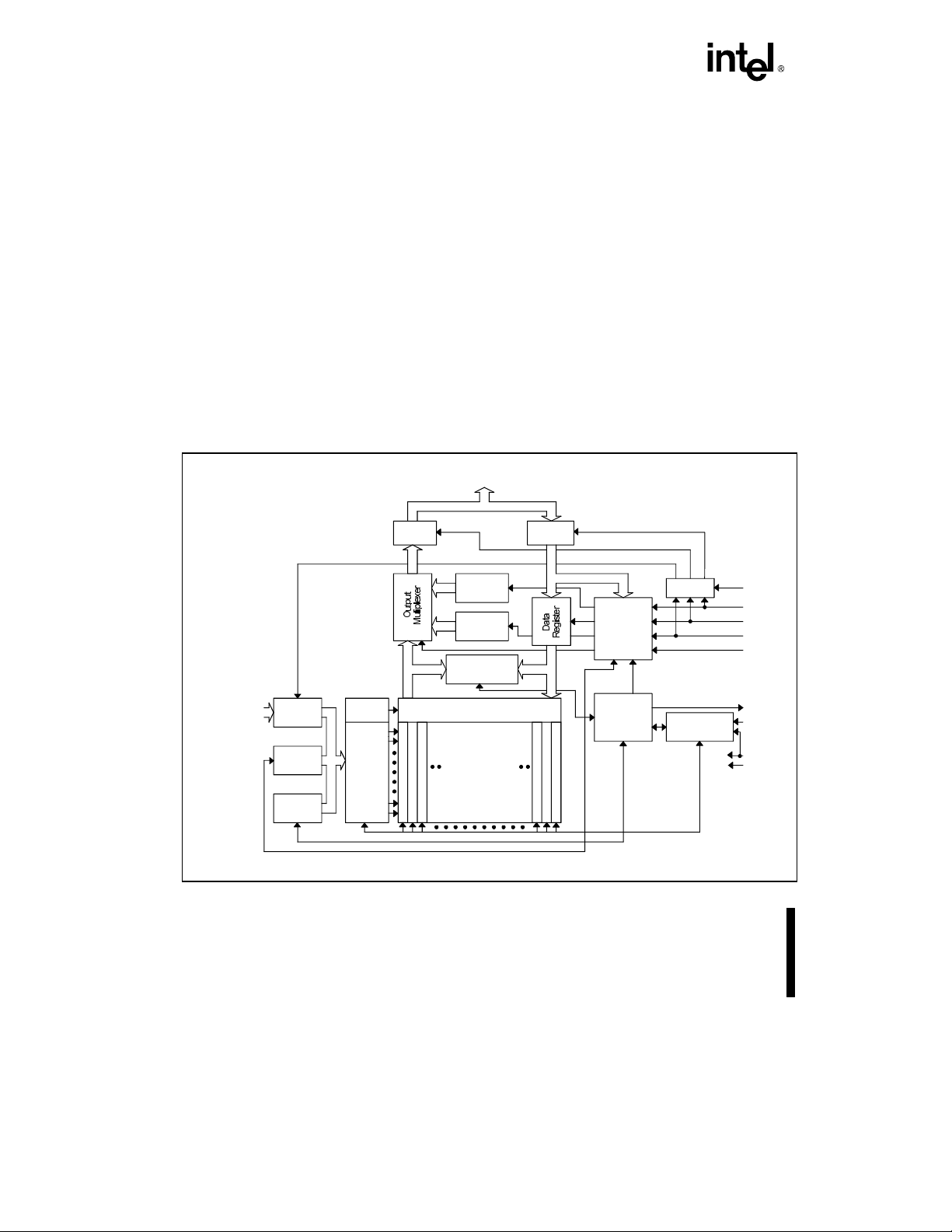
Output
Buffer
The Automatic Power Savings (APS) feature
substantially reduces active current when the
device is in static mode (addresses not switching).
In APS mode, the typical I
current is 1 mA.
CCR
When CE# and RP# pins are at VCC, the
component enters a CMOS standby mode. Driving
RP# to GND enables a deep power-down mode
which significantly reduces power consumption,
provides write protection, resets the device, and
clears the status register. A reset time (t
required from RP# switching high until outputs are
valid. Likewise, the device has a wake time (t
from RP#-high until writes to the CUI are
recognized.
1.3 Pinout and Pin Description
The family of devices is available in 40-lead TSOP
(Thin Small Outline Package, 1.2 mm thick) and
44-lead PSOP (Plastic Small Outline Package).
Pinouts are shown in Figures 2 and 3.
DQ - DQ
0 7
Input
Buffer
PHQV
) is
PHEL
)
4-Mbit: A - A ,
0
8-Mbit: A - A ,
0
16-Mbit: A - A
0 20
6
Identifier
Register
Status
Register
Data
Comparator
18
Input
19
Buffer
Address
Latch
Address
Counter
Y
Decoder
X
Decoder
Y Gating
4-Mbit: Eight
8-Mbit: Sixteen
16-Mbit: Thirty-Two
64-Kbyte Blocks
Command
Register
Write State
Machine
I/O Logic
Program/Erase
Voltage Switch
V
CC
CE#
WE#
OE#
RP#
RY/BY#
V
PP
V
CC
GND
Figure 1. Block Diagram
PRODUCT PREVIEW

E BYTE-WIDE SMART 5 FlashFile™ MEMORY FAMILY
K
Table 1. Pin Descriptions
Sym Type Name and Function
A0–A
DQ0–DQ7INPUT/
CE# INPUT CHIP ENABLE: Activates the device’s control logic, input buffers, decoders, and
RP# INPUT RESET/DEEP POWER-DOWN: When driven low, RP# inhibits write operations
OE# INPUT OUTPUT ENABLE: Gates the device’s outputs during a read cycle.
WE# INPUT WRITE ENABLE: Controls writes to the CUI and array blocks. Addresses and data
RY/BY# OUTPUT READY/BUSY#: Indicates the status of the internal WSM. When low, the WSM is
V
PP
V
CC
GND SUPPLY GROUND: Do not float any ground pins.
NC NO CONNECT: Lead is not internally connected; it may be driven or floated.
INPUT ADDRESS INPUTS: Inputs for addresses during read and write operations.
20
OUTPUT
SUPPLY BLOCK ERASE, PROGRAM, LOCK-BIT CONFIGURATION POWER SUPPLY:
SUPPLY DEVICE POWER SUPPLY: Internal detection automatically configures the device
Addresses are internally latched during a write cycle.
4Mbit → A
16Mbit → A0–A
DATA INPUT/OUTPUTS: Inputs data and commands during CUI write cycles;
outputs data during memory array, status register, and identifier code read cycles.
Data pins float to high-impedance when the chip is deselected or outputs are
disabled. Data is internally latched during a write cycle.
sense amplifiers. CE#-high deselects the device and reduces power consumption to
standby levels.
which provides data protection during power transitions, puts the device in deep
power-down mode, and resets internal automation. RP#-high enables normal
operation. Exit from deep power-down sets the device to read array mode.
RP# at V
lock-bits when the master lock-bit is set. RP# = V
thereby enabling block erase and program operations to locked memory blocks.
Block erase, program, or lock-bit configuration with V
spurious results and should not be attempted.
are latched on the rising edge of the WE# pulse.
performing an internal operation (block erase, program, or lock-bit configuration).
RY/BY#-high indicates that the WSM is ready for new commands, block erase or
program is suspended, or the device is in deep power-down mode. RY/BY# is
always active.
For erasing array blocks, programming data, or configuring lock-bits.
With VPP ≤ V
lock-bit configuration with an invalid V
results and should not be attempted.
for optimized read performance. Do not float any power pins.
With VCC ≤ V
operations at invalid V
results and should not be attempted.
8Mbit → A
enables setting of the master lock-bit and enables configuration of block
HH
Smart 5 Flash → 5V and 12V V
, memory contents cannot be altered. Block erase, program, and
PPL
Smart 5 Flash → 5V V
, all write attempts to the flash memory are inhibited. Device
LKO
–A
–A
20
overrides block lock-bits,
HH
< RP# < VHH produce
IH
PP
(see DC Characteristics) produce spurious
PP
CC
voltages (see DC Characteristics) produce spurious
CC
PRODUCT PREVIEW
7

BYTE-WIDE SMART 5 FlashFile™ MEMORY FAMILY E
28F016S5
28F008S5
28F004S5
A
19A19
A
18
A
17
A
16
A
15
A
14
A
13
A
12
CE#
V
CC
V
PP
RP#
A
11
A
10
A
9
A
8
A
7
A
6
A
5
A
4
A
A
A
A
A
A
A
CE#
V
V
RP#
A
A
A
A
A
A
A
A
NC
A
18
18
A
17
17
A
16
16
A
15
15
A
14
14
A
13
13
A
12
12
CE#
V
CC
CC
V
PP
PP
RP#
A
11
11
A
10
10
A
9
9
A
8
8
A
7
7
A
6
6
A
5
5
A
4
4
1
2
3
4
5
6
7
8
9
10
11
12
13
14
15
16
17
18
19
20
40-LEAD TSOP
STANDARD PINOUT
10 mm x 20 mm
TOP VIEW
40
39
38
37
36
35
34
33
32
31
30
29
28
27
26
25
24
23
22
21
NC
NC
WE#
OE#
RY/BY#
DQ
DQ
DQ
DQ
V
CC
GND
GND
DQ
DQ
DQ
DQ
A
0
A
1
A
2
A
3
WE#
OE#
RY/BY#
DQ
7
DQ
6
DQ
5
DQ
4
V
GND
GND
DQ
3
DQ
2
DQ
1
DQ
0
Figure 2. TSOP 40-Lead Pinout
28F016S5
28F008S5
28F004S5
V
RP#
A
A
A
A
A
A
NC
NC
A
A
A
DQ
DQ
DQ
DQ
GND
GND
V
PP
RP#
A
11
10
A
9
8
7
6
5
4
NC
NC
A
3
2
1
0
DQ
0
DQ
1
DQ
2
DQ
3
GND
GND
V
PP
RP#
A
A
A
A
A
A
A
A
A
A
A
A
A
11
A
10
A
9
A
8
A
7
A
6
A
5
A
4
NC
NC
A
3
A
2
A
1
A
0
DQ
0
DQ
1
DQ
2
DQ
3
GND
GND
1
PP
2
3
11
4
10
5
9
6
8
7
7
8
6
9
5
4
3
2
1
0
0
1
2
3
44-LEAD PSOP
10
13.3 mm x 28.2 mm
11
12
13
14
15
16
17
18
19
20
TOP VIEW
21
22
44
43
42
41
40
39
38
37
36
35
34
33
32
31
30
29
28
27
26
25
24
23
V
CC
CE#
A
12
A
13
A
14
A
15
A
16
A
17
A
18
NC
NC
NC
NC
NC
WE#
OE#
RY/BY#
DQ
DQ
DQ
DQ
V
CC
V
CE#
A
A
A
A
A
A
A
A
NC
NC
NC
NC
WE#
OE#
RY/BY#
DQ
7
DQ
6
DQ
5
DQ
4
V
CC
CC
V
CC
CE#
A
12
13
14
15
16
17
18
19
12
A
13
A
14
A
15
A
16
A
17
A
18
A
19
A
20
NC
NC
NC
WE#
OE#
RY/BY#
DQ
7
6
5
4
DQ
DQ
DQ
V
CC
7
6
5
4
NC
NC
A
A
A
A
A
20
NC
WE#
OE#
RY/BY#
DQ
7
7
DQ
6
6
DQ
5
5
DQ
4
4
V
CC
CC
GND
GND
DQ
3
3
DQ
2
2
DQ
1
1
DQ
0
0
A
0
0
A
1
1
A
2
2
A
3
3
Figure 3. PSOP 44-Lead Pinout
8
PRODUCT PREVIEW
E BYTE-WIDE SMART 5 FlashFile™ MEMORY FAMILY
2.0 PRINCIPLES OF OPERATION
The byte-wide Smart 5 FlashFile memories include
an on-chip WSM to manage block erase, program,
and lock-bit configuration functions. It allows for:
100% TTL-level control inputs, fixed power s upplies
during block erasure, program, and lock-bit
configuration, and minimal process or overhead with
RAM-like interface timings.
After initial device power-up or return from deep
power-down mode (see Bus Operations), the
device defaults to read array mode. Mani pulation of
external memory control pins allow array read,
standby, and output disable operations.
Status register and identifier codes can be
accessed through the CUI independent of the V
voltage. High voltage on VPP enables successful
block erasure, program, and lock-bit c onfiguration.
All functions associated with altering memory
contents—block erase, program, lock-bit
configuration, status, and identifier codes—are
accessed via the CUI and verified through the
status register.
Commands are written using standard microprocessor write timings . The CUI c ontents s erve as
input to the WSM that controls block erase,
program, and lock-bit configuration operat ions. The
internal algorithms are regulated by the WSM,
including pulse repetition, internal verification, and
margining of data. Addresses and data are
internally latched during write cycles. Writing the
appropriate command outputs array data, acces ses
the identifier codes, or outputs status register data.
Interface software that initiates and polls progress
of block erase, program, and lock-bit configuration
can be stored in any block. This code is c opied to
and executed from system RAM during flash
memory updates. After successful completion,
reads are again possible via the Read Array
command. Block erase suspend allows system
software to suspend a block erase to read data
from or program data to any other block . Program
suspend allows system software to suspend a
program to read data from any other flash memory
array location.
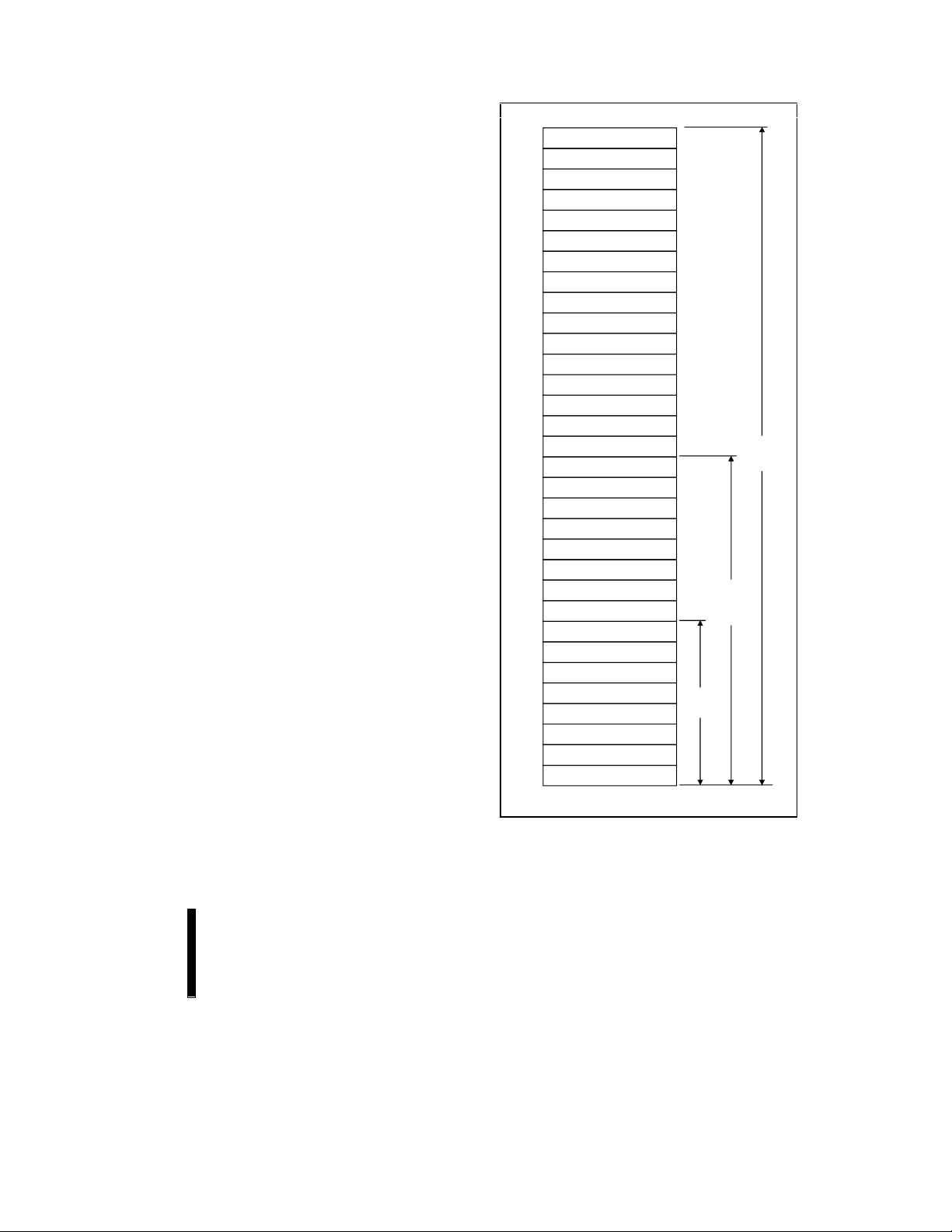
1FFFFF
1F0000
1EFFFF
1E0000
1DFFFF
1D0000
1CFFFF
1C0000
1BFFFF
1B0000
1AFFFF
1A0000
19FFFF
190000
18FFFF
180000
17FFFF
170000
16FFFF
160000
15FFFF
PP
150000
14FFFF
140000
13FFFF
130000
12FFFF
120000
11FFFF
110000
10FFFF
100000
0FFFFF
0F0000
0EFFFF
0E0000
0DFFFF
0D0000
0CFFFF
0C0000
0BFFFF
0B0000
0AFFFF
0A0000
09FFFF
090000
08FFFF
080000
07FFFF
070000
06FFFF
060000
05FFFF
050000
04FFFF
040000
03FFFF
030000
02FFFF
020000
01FFFF
010000
00FFFF
000000
64-Kbyte Block
64-Kbyte Block
64-Kbyte Block
64-Kbyte Block
64-Kbyte Block
64-Kbyte Block
64-Kbyte Block
64-Kbyte Block
64-Kbyte Block
64-Kbyte Block
64-Kbyte Block
64-Kbyte Block
64-Kbyte Block
64-Kbyte Block
64-Kbyte Block
64-Kbyte Block
64-Kbyte Block
64-Kbyte Block
64-Kbyte Block
64-Kbyte Block
64-Kbyte Block
64-Kbyte Block
64-Kbyte Block
64-Kbyte Block
64-Kbyte Block
64-Kbyte Block
64-Kbyte Block
64-Kbyte Block
64-Kbyte Block
64-Kbyte Block
64-Kbyte Block
64-Kbyte Block
31
30
29
28
27
26
25
24
23
22
21
20
19
18
17
16
15
14
13
12
11
10
9
8
7
6
5
4
4-Mbit
3
2
1
0
16-Mbit
8-Mbit
PRODUCT PREVIEW
Figure 4. Memory Map
9

BYTE-WIDE SMART 5 FlashFile™ MEMORY FAMILY E
2.1 Data Protection
Depending on the application, the system designer
may choose to make the V
power supply
PP
switchable (available only when memory block
erases, programs, or lock-bit configurations are
required) or hardwired to V
. The device
PPH1/2
accommodates either design practice and
encourages optimization of the processor-memory
interface.
When V
altered. When high voltage is applied to V
PP
≤ V
, memory contents cannot be
PPLK
PP
, the
two-step block erase, program, or lock-bit
configuration command sequences provides protection from unwanted operations. All write
functions are disabled when V
the write lockout voltage V
V
. The device’s block locking capability provides
IL
voltage is below
CC
or when RP# is at
LKO
additional protection from i nadvertent code or data
alteration by gating erase and program operations.
3.0 BUS OPERATION
The local CPU reads and writes flash memory
in-system. All bus cycles to or from the flash
memory conform to standard microprocessor bus
cycles.
3.1 Read
3.2 Output Disable
With OE# at a logic-high level (VIH), the device
outputs are disabled. Output pins DQ
–DQ7 are
0
placed in a high-impedance state.
3.3 Standby
CE# at a logic-high level (VIH) places the device in
standby mode which substantially reduces device
power consumption. DQ
–DQ7 outputs are placed
0
in a high-impedance state independent of OE#. If
deselected during block erase, program, or
lock-bit configuration, the device continues
functioning and consuming active power until the
operation completes.
3.4 Deep Power-Down
RP# at VIL initiates the deep power-down mode.
In read mode, RP#-low deselects the memory,
places output drivers in a high-impedance state,
and turns off all internal c ircuits. RP# mus t be held
low for time t
return from power-down until initial m emory access
outputs are valid. After this wake-up interval,
normal operation is restored. The CUI resets to
read array mode, and the status register is set to
80H.
PLPH
. Time t
is required after
PHQV
Block information, i dentifier codes, or status register
can be read independent of the V
can be at either V
or VHH.
IH
voltage. RP#
PP
The first task is to write the appropri ate read-mode
command (Read Array, Read Identifier Codes, or
Read Status Register) to the CUI. Upon initial
device power-up or after exit from deep powerdown mode, the device automati cally resets to read
array mode. Four control pins dictate the data flow
in and out of the component: CE#, OE#, WE#, and
RP#. CE# and OE# must be driven active to obtai n
data at the outputs. CE# is the device selection
control, and when active enables the selected
memory device. OE# is the data out put (DQ
–DQ7)
0
control and when active drives the selected
memory data onto the I/O bus . WE # mus t be at V
and RP# must be at VIH or VHH. Figure 15
illustrates a read cycle.
10
During block erase, program, or lock-bit
configuration, RP#-low will abort the operation.
RY/BY# remains low until the reset operation is
complete. Memory contents being altered are no
longer valid; the data may be partially erased or
written. Time t
logic-high (V
written.
is required after RP# goes to
PHWL
) before another command can be
IH
As with any automated device, it is important to
assert RP# during system reset. When the system
comes out of reset, i t ex pect s t o read from t he flas h
memory. Automated flash memori es provide status
information when accessed during block erase,
program, or lock-bit confi guration modes. If a CPU
reset occurs with no flash memory reset, proper
CPU initialization m ay not occur because the flas h
IH
memory may be providing status information
instead of array data. Int el’s flash memories allow
proper CPU initialization following a system reset
through the use of the RP# input. In this applic ation,
RP# is controlled by the same RESET# signal that
resets the system CPU.
PRODUCT PREVIEW
E BYTE-WIDE SMART 5 FlashFile™ MEMORY FAMILY
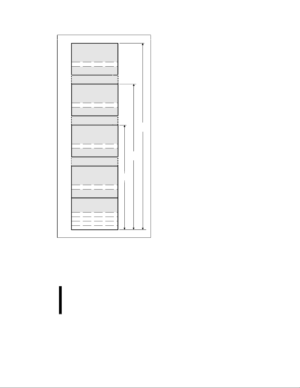
1FFFFF
Future Implementation
1F0002
Block 31 Lock Configuration
1F0000
0FFFFF
0F0002
0F0000
07FFFF
070002
070000
01FFFF
010002
010000
00FFFF
000003
000002
000001
000000
Future Implementation
(Blocks 16 through 30)
Future Implementation
Block 15 Lock Configuration
Future Implementation
(Blocks 8 through 14)
Reserved for
Future Implementation
Block 7 Lock Configuration
Future Implementation
(Blocks 2 through 14)
Future Implementation
Block 1 Lock Configuration
Future Implementation
Future Implementation
Master Lock Configuration
Block 0 Lock Configuration
Device Code
Manufacturer Code
Reserved for
Reserved for
Reserved for
Reserved for
Reserved for
Reserved for
Reserved for
Reserved For
Block 31
Block 15
Block 7
Block 1
Block 0
4-Mbit
8-Mbit
16-Mbit
3.5 Read Identifier Codes Operation
The read identifier codes operation outputs the
manufacturer code, device code, block lock
configuration codes for each bloc k, and mas ter loc k
configuration code (see Figure 5). Using the
manufacturer and device codes, the system
software can automatic al l y match the device wit h i ts
proper algorithms. The block lock and master lock
configuration codes identify locked and unlocked
blocks and master lock-bit setting.
3.6 Write
The CUI does not occupy an address able memory
location. It is wri tten when WE# and CE# are act ive
and OE# = V
. The address and data needed to
IH
execute a command are latched on the risi ng edge
of WE# or CE# (whichever goes high first).
Standard microprocessor write timings are used.
Figure 17 illustrates a write operation.
4.0 COMMAND DEFINITIONS
When the VPP voltage ≤ V
from the status register, identif ier codes, or blocks
are enabled. Placing V
successful block erase, program, and lock-bit
configuration operations.
Device operations are selected by writing specific
commands into the CUI. Table 3 defines these
commands.
, read operations
PPLK
on VPP enables
PPH1/2
Figure 5. Device Identifier Code Memory Map
PRODUCT PREVIEW
11

BYTE-WIDE SMART 5 FlashFile™ MEMORY FAMILY E
Table 2. Bus Operations
Mode Notes RP# CE# OE# WE# Address V
Read 1,2,3 VIH or
V
Output Disable 3 VIH or
V
Standby 3 VIH or
V
Deep Power-Down 4 V
Read Identifier Codes VIH or
V
Write 3,6,7 VIH or
V
NOTES:
1. Refer to DC Characteristics. When V
2. X can be V
V
PPH1/2
3. RY/BY# is V
or VIH for control and address input pins and V
IL
voltages.
when the WSM is executing internal block erase, program, or lock-bit configuration algorithms. It is V
OL
when the WSM is not busy, in block erase suspend mode (with program inactive), program suspend mode, or deep powerdown mode.
4. RP# at GND ± 0.2V ensures the lowest deep power-down current.
5. See Section 4.2 for read identifier code data.
6. Command writes involving block erase, program, or lock-bit configuration are reliably executed when V
V
= V
CC
7. Refer to Table 3 for valid D
(see Section 6.2 for operating conditions).
CC1/2
during a write operation.
IN
≤ V
PP
V
HH
V
HH
V
HH
IL
V
HH
V
HH
, memory contents can be read, but not altered.
PPLK
V
IL
V
IL
IH
V
IL
IH
IH
V
IH
XXD
X X High Z X
X X X X High Z X
X X X X X High Z V
V
IL
V
IL
PPLK
V
IL
V
IH
or V
PPH1/2
See
IH
Figure 5
IL
XXDINX
for VPP. See DC Characteristics for V
PP
DQ
OUT
0–7
RY/BY#
X Note 5 V
PPLK
= V
PP
PPH1/2
X
OH
OH
and
OH
and
12
PRODUCT PREVIEW
 Loading...