*Other brands and names are the property of their respective owners.
Information in this document is provided in connection with Intel products. Intel assumes no liability whatsoever, including infringement of any patent or
copyright, for sale and use of Intel products except as provided in Intel’s Terms and Conditions of Sale for such products. Intel retains the right to make
changes to these specifications at any time, without notice. Microcomputer Products may have minor variations to this specification known as errata.
October 1995COPYRIGHT©INTEL CORPORATION, 1995 Order Number: 272335-003
87C51/80C51BH/80C31BH
CHMOS SINGLE-CHIP 8-BIT MICROCONTROLLER
Commercial/Express
87C51/80C51BH/80C51BHP/80C31BH
*See Table 1 for Proliferation Options
Y
High Performance CHMOS EPROM
Y
24 MHz Operation
Y
Improved Quick-Pulse Programming
Algorithm
Y
3-Level Program Memory Lock
Y
Boolean Processor
Y
128-Byte Data RAM
Y
32 Programmable I/O Lines
Y
Two 16-Bit Timer/Counters
Y
Extended Temperature Range
(
b
40§Ctoa85§C)
Y
5 Interrupt Sources
Y
Programmable Serial Port
Y
TTL- and CMOS-Compatible Logic
Levels
Y
64K External Program Memory Space
Y
64K External Data Memory Space
Y
ONCE Mode Facilitates System Testing
Y
Power Control Modes
Ð Idle
Ð Power Down
MEMORY ORGANIZATION
PROGRAM MEMORY: Up to 4 Kbytes of the program memory can reside on-chip (except 80C31BH). In
addition the device can address up to 64K of program memory external to the chip.
DATA MEMORY: This microcontroller has a 128 x 8 on-chip RAM. In addition it can address up to 64 Kbytes of
external data memory.
The Intel 87C51/80C51BH/80C31BH is a single-chip control-oriented microcontroller which is fabricated on
Intel’s reliable CHMOS III-E technology. Being a member of the MCS
É
51 controller family, the
87C51/80C51BH/80C31BH uses the same powerful instruction set, has the same architecture, and is pin-forpin compatible with the existing MCS 51 controller family of products.
The 80C51BHP is identical to the 80C51BH. When ordering the 80C51BHP, customers must submit the 64
byte encryption table together with the ROM code. Lock bit 1 will be set to enable the internal ROM code
protection and at the same time allows code verification.
The extremely low operating power, along with the two reduced power modes, Idle and Power Down, make
this part very suitable for low power applications. The Idle mode freezes the CPU while allowing the RAM,
timer/counters, serial port and interrupt system to continue functioning. The Power Down mode saves the
RAM contents but freezes the oscillator, causing all other chip functions to be inoperative.
For the remainder of this document, the 87C51, 80C51BH, and 80C31BH will be referred to as the 87C51/BH,
unless information applies to a specific device.

87C51/80C51BH/80C31BH
Table 1. Proliferation Options
*Standard -1 -2 -24
80C31BH X X X X
80C51BH X X X X
80C51BHP X X X X
87C51 X X X X
NOTES:
* 3.5 MHz to 12 MHz; V
CC
e
5Vg20%
-1 3.5 MHz to 16 MHz; V
CC
e
5Vg20%
-2 0.5 MHz to 12 MHz; V
CC
e
5Vg20%
-24 3.5 MHz to 24 MHz; V
CC
e
5Vg20%
272335– 1
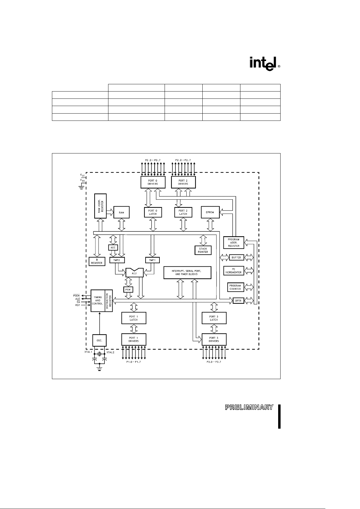
Figure 1. 87C51/BH Block Diagram
2

87C51/80C51BH/80C31BH
PROCESS INFORMATION
The 87C51/BH is manufactured on the CHMOS III-E
process. Additional process and reliability information is available in Intel’s
Components Quality and
Reliability Handbook,
Order No. 210997.
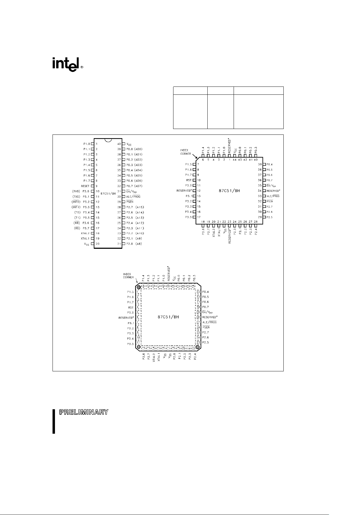
PACKAGES
Part Prefix Package Type
87C51/BH P 40-Pin Plastic
DIP (OTP)
D 40-Pin CERDIP
(EPROM)
N 44-Pin PLCC (OTP)
S 44-Pin QFP (OTP)
272335– 2
DIP
272335– 3
PLCC
272335– 4
*Do not connect reserved pins. QFP
Figure 2. Pin Connections
3

87C51/80C51BH/80C31BH
PIN DESCRIPTION
VCC: Supply voltage during normal, Idle and Power
Down operations.
V
SS
: Circuit ground.
Port 0: Port 0 is an 8-bit open drain bidirectional I/O
port. As an output port each pin can sink several LS
TTL inputs. Port 0 pins that have 1’s written to them
float, and in that state can be used as high-impedance inputs.
Port 0 is also the multiplexed low-order address and
data bus during accesses to external memory. In this
application it uses strong internal pullups when emitting 1’s.
Port 0 also receives the code bytes during EPROM
programming, and outputs the code bytes during
program verification. External pullups are required
during program verification.
Port 1: Port 1 is an 8-bit bidirectional I/O port with
internal pullups. The Port 1 output buffers can drive
LS TTL inputs. Port 1 pins that have 1’s written to
them are pulled high by the internal pullups, and in
that state can be used as inputs. As inputs, Port 1
pins that are externally pulled low will source current
(I
IL
, on the data sheet) because of the internal pull-
ups.
Port 1 also receives the low-order address bytes
during EPROM programming and program verification.
Port 2: Port 2 is an 8-bit bidirectional I/O port with
internal pullups. Port 2 pins that have 1’s written to
them are pulled high by the internal pullups, and in
that state can be used as inputs. As inputs, Port 2
pins that are externally pulled low will source current
(I
IL
, on the data sheet) because of the internal pull-
ups.
Port 2 emits the high-order address byte during
fetches from external Program memory and during
accesses to external Data Memory that use 16-bit
address (MOVX
@
DPTR). In this application it uses
strong internal pullups when emitting 1’s.
During accesses to external Data Memory that use
8-bit addresses (MOVX
@
Ri), Port 2 emits the con-
tents of the P2 Special Function Register.
Port 2 also receives some control signals and the
high-order address bits during EPROM programming
and program verification.
Port 3: Port 3 is an 8-bit bidirectional I/O port with
internal pullups. The Port 3 output buffers can drive
LS TTL inputs. Port 3 pins that have 1’s written to
them are pulled high by the internal pullups, and in
that state can be used as inputs. As inputs, Port 3
pins that are externally pulled low will source current
(I
IL
, on the data sheet) because of the pullups.
Port 3 also serves the functions of various special
features of the MCS-51 Family, as listed below:
Pin Name Alternate Function
P3.0 RXD Serial input line
P3.1 TXD Serial output line
P3.2 INT0 External Interrupt 0
P3.3 INT1
External Interrupt 1
P3.4 T0 Timer 0 external input
P3.5 T1 Timer 1 external input
P3.6 WR
External Data Memory Write strobe
P3.7 RD
External Data Memory Read strobe
Port 3 also receives some control signals for
EPROM programming and program verification.
RST: Reset input. A high on this pin for two machine
cycles while the oscillator is running resets the device. The port pins will be driven to their reset condition when a minimum V
IH1
voltage is applied whether the oscillator is running or not. An internal pulldown resistor permits a power-on reset with only a
capacitor connected to V
CC
.
ALE/PROG
: Address Latch Enable output signal for
latching the low byte of the address during accesses
to external memory. This pin is also the program
pulse input (PROG
) during EPROM programming for
the 87C51.
If desired, ALE operation can be disabled by setting
bit 0 of SFR location 8EH. With this bit set, the pin is
weakly pulled high. However, the ALE disable feature will be suspended during a MOVX or MOVC instruction, idle mode, power down mode and ICE
mode. The ALE disable feature will be terminated by
reset. When the ALE disable feature is suspended or
terminated, the ALE pin will no longer be pulled up
weakly. Setting the ALE-disable bit has no effect if
the microcontroller is in external execution mode.
4

87C51/80C51BH/80C31BH
In normal operation ALE is emitted at a constant
rate of 1/6 the oscillator frequency, and may be
used for external timing or clocking purposes. Note,
however, that one ALE pulse is skipped during each
access to external Data Memory.
PSEN
: Program Store Enable is the Read strobe to
External Program Memory. When the 87C51/BH is
executing from Internal Program Memory, PSEN
is
inactive (high). When the device is executing code
from External Program Memory, PSEN
is activated
twice each machine cycle, except that two PSEN
activations are skipped during each access to External Data Memory.
EA
/VPP: External Access enable. EA must be
strapped to V
SS
in order to enable the 87C51/BH to
fetch code from External Program Memory locations
starting at 0000H up to FFFFH. Note, however, that
if either of the Lock Bits is programmed, the logic
level at EA
is internally latched during reset.
EA
must be strapped to VCCfor internal program
execution.
This pin also receives the programming supply voltage (VPP) during EPROM programming.
XTAL1: Input to the inverting oscillator amplifier.
XTAL2: Output from the inverting oscillator amplifi-
er.
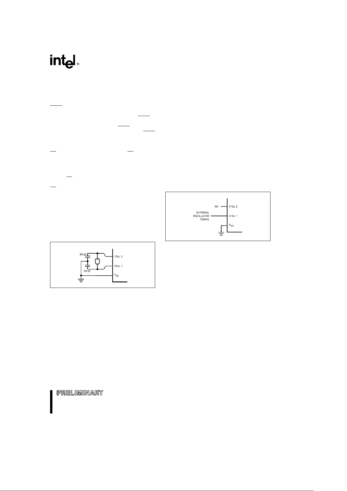
272335– 5
Figure 3. Using the On-Chip Oscillator
OSCILLATOR CHARACTERISTICS
XTAL1 and XTAL2 are the input and output, respectively, of an inverting amplifier which can be configured for use as an on-chip oscillator, as shown in
Figure 3.
To drive the device from an external clock source,
XTAL1 should be driven, while XTAL2 is left unconnected, as shown in Figure 4. There are no requirements on the duty cycle of the external clock signal,
since the input to the internal clocking circuitry is
through a divide-by-two flip-flop, but minimum and
maximum high and low times specified on the data
sheet must be observed.
An external oscillator may encounter as much as a
100 pF load at XTAL1 when it starts up. This is due
to interaction between the amplifier and its feedback
capacitance. Once the external signal meets the V
IL
and VIHspecifications the capacitance will not exceed 20 pF.
272335– 6
Figure 4. External Clock Drive
5

87C51/80C51BH/80C31BH
IDLE MODE
In Idle Mode, the CPU puts itself to sleep while all
the on-chip peripherals remain active. The mode is
invoked by software. The content of the on-chip
RAM and all the Special Functions Registers remain
unchanged during this mode. The Idle Mode can be
terminated by any enabled interrupt or by a hardware reset.
It should be noted that when Idle is terminated by a
hardware reset, the device normally resumes program execution, from where it left off, up to two machine cycles before the internal reset algorithm
takes control. On-chip hardware inhibits access to
internal RAM in this event, but access to the port
pins is not inhibited. To eliminate the possibility of an
unexpected write to a port pin when Idle is terminated by reset, the instruction following the one that
invokes Idle should not be one that writes to a port
pin or to external memory.
POWER DOWN MODE
To save even more power, a Power Down mode can
be invoked by software. In this mode, the oscillator
is stopped and the instruction that invoked Power
Down is the last instruction executed. The on-chip
RAM and Special Function Registers retain their values until the Power Down mode is transmitted.
On the 87C51/BH either a hardware reset or an external interrupt can cause an exit from Power Down.
Reset redefines all the SFR’s but does not change
the on-chip RAM. An external interrupt allows both
the SFRs and on-chip RAM to retain their values.
To properly terminate Power Down, the reset or external interrupt should not be executed before V
CC
is
restored to its normal operating level, and must be
held active long enough for the oscillator to restart
and stabilize (normally less than 10 ms).
With an external interrupt INT0 and INT1 must be
enabled and configured as level-sensitive. Holding
the pin low restarts the oscillator but bringing the pin
back high completes the exit. Once the interrupt is
serviced, the next instruction to be executed after
RET1 will be the one following the instruction that
put the device into Power Down.
DESIGN CONSIDERATIONS
#
Exposure to light when the device is in operation
may cause logic errors. For this reason, it is suggested that an opaque label be placed over the
window when the die is exposed to ambient light.
#
The 87C51/BH now have some additional features. The features are: asynchronous port reset,
4 interrupt priority levels, power off flag, ALE disable, serial port automatic address recognition,
serial port framing error detection, 64-byte encryption array, and 3 program lock bits. These
features cannot be used with the older versions
of 80C51BH/80C31BH. The newer version of
80C51BH/80C31BH will have change identifier
‘‘A’’ appended to the lot number.
Table 2. Status of the External Pins during Idle and Power Down
Mode
Program
ALE PSEN PORT0 PORT1 PORT2 PORT3
Memory
Idle Internal 1 1 Data Data Data Data
Idle External 1 1 Float Data Address Data
Power Down Internal 0 0 Data Data Data Data
Power Down External 0 0 Float Data Data Data
6

87C51/80C51BH/80C31BH
ONCE MODE
The ONCE (‘‘On-Circuit Emulation’’) mode facilitates
testing and debugging of systems using the
87C51/BH without the 87C51/BH having to be removed from the circuit. The ONCE mode is invoked
by:
1. Pull ALE low while the device is in reset and
PSEN
is high;
2. Hold ALE low as RST is deactivated.
While the device is in ONCE mode, the Port 0 pins
float, and the other port pins and ALE and PSEN
are
weakly pulled high. The oscillator circuit remains active. While the 87C51/BH is in this mode, an emulator or test CPU can be used to drive the circuit. Normal operation is restored when a normal reset is applied.
87C51/BH EXPRESS
The Intel EXPRESS system offers enhancements to
the operational specifications of the MCS-51 family
of microcontrollers. These EXPRESS products are
designed to meet the needs of those applications
whose operating requirements exceed commercial
temperature.
The EXPRESS program includes the commercial
standard temperature range with burn-in and an extended temperature range with or without burn-in.
With the commercial standard temperature range,
operational characteristics are guaranteed over the
temperature range of 0
§
Cto70§C. With the extended temperature range option, operational characteristics are guaranteed over the range of
b
40§Cto
a
85§C.
The optional burn-in is dynamic for a minimum time
of 160 hours at 125
§
C with V
CC
e
6.9Vg0.25V,
following guidelines in MIL-STD-883, Method 1015.
Package types and EXPRESS versions are identified
by a one- or two-letter prefix to the part number. The
prefixes are listed in Table 3.
For the extended temperature range option, this
data sheet specifies the parameters which deviate
from their commercial temperature range limits.
Table 3. Prefix Identification
Prefix
Package Temperature
Burn-in
Type Range
P Plastic Commercial No
D Cerdip Commercial No
N PLCC Commercial No
S QFP Commercial No
TP Plastic Extended No
TD Cerdip Extended No
TN PLCC Extended No
TS QFP Extended No
LP Plastic Extended Yes
LD Cerdip Extended Yes
LN PLCC Extended Yes
NOTE:
Contact distributor or local sales office to match EXPRESS
prefix to proper device.
Examples:
P87C51 indicates 87C51 in a plastic package and
specified for commercial temperature range, without
burn-in.
LD87C51 indicates 87C51 in a cerdip package and
specified for extended temperature range with burnin.
7
 Loading...