

Page 1

Information in this document is provided in connection with Intel products. Intel assumes no liability whatsoever, including infringement of
any patent or copyright, for sale and use of Intel products except as provided in Intel’s Terms and Conditions of Sale for such products.
Intel retains the right to make changes to these specifications at any time, without notice. Microcontroller products may have minor variations to this specification known as errata.
COPYRIGHT © INTEL CORPORATION, 1996 March 1996 Order Number: 272800-001
83C51KB
HIGH PERFORMANCE
KEYBOARD MICROCON TRO LLER
The 83C51KB is a highly integrated keyboard microcontroller for the standard and advanced desktop
keyboard industry. The integration of external components into the microcont roller reduces overall keyboard
control system manufactur ing cost in terms of the number of components used, the amount of PCB space
required, reduced inventory, and a reduction in required assembly activities. In addition, the integration
reduces the number and amount of software routines needed for signal debounce and input status poll
operation. There is a resultant reduction in CPU overhead as well as on-chip memory requirements. The
83C51KB product line is manufactured w ith Intel state of the art complimentary high-p erformance metallic
oxide semiconductor (CHMOS) design rules.
■ Direct Drive LED Outputs
—Four Pins (P3.7:4)
—13 mA Typical Current Sink
Capability
■ 20 pF Cap On-chip for RC Resonator
—Frequency Selectable (4-6 MHz)
■ 8 Dedicated Key Scan Input (KSI) Pins
—Schmitt-trigger Inputs
—External Interrupt
—Level Detect Interrupt Mode for
Automatic Power-down Exit
■ 16 Dedicated Key Scan Output (KSO)
Pins with Quasi-bidirectional Port
Drivers
—No External Resistor Required
—Located on P0.7:0 and P2.7:0
■ 4-Kbyte On-chip ROM Memory
■ 128-byte On-chip RAM Memory
■ Clock/Data Drivers to Motherboard
—Strong Pullup Drivers for Keyboard
Cable Communication
—8X42 Compatible Interface
—Selectable external interrup t for
Clock
■ ONCE mode (On-chip Emulation)
■ Power-on Reset Mode
—Automatic Operation
■ 5 Volt D.C. Operation
■ Reduces Manufacturing Cost by
Reducing Overall Component Count
■ Configurable Timer (16 bit or 2 by 8 Bit)
■ Uses Industry Standard Design Tools
■ Control Oriented Instruction Set
■ Industry Standard Architecture
Page 2
2
83C51KB HIGH PERFORMANCE KEYBO ARD M ICRO CO NT RO L LE R
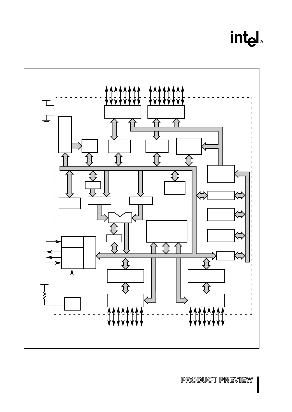
Figure 1. 83C51KB Block Diagram
Port 0
Drivers
KSO 0–7
P0.0 – P0.7
Port 0
Latch
Port 0
Drivers
KSO 8–15
P2.0 – P2.7
Port 2
Latch
ROM
Program
Address
Register
Buffer
RAM
Address Register
RAM
ACC
TMP2
Stack
Pointer
PC
Incrementer
Program
Counter
DPTR
TMP1
A3350-01
CLK, Data, LED 0–3
P3.0 – P3.7
ALU
PSW
Timing
and
Control
Instruction
Register
Power On
Reset Ctrl.
B
Register
SFRs
Timer
Port 3
Latch
Port 3
Drivers
KSI 0–7
P1.0 – P1.7
Port 1
Latch
Port 1
Drivers
RC
Osc.
RST
PSEN#
ALE
EA#
V
CC
V
SS
V
CC
Page 3
3
83C51KB HIGH PERFORMANCE KEYBOARD MICROCONTROLLER
1.0 TEMPERATURE RANGE
With the commercial (standard) temperature
marking, this product line operates over the temperature range 0°C to +70°C.
2.0 PROCESS INFORMATION
This device is manufactured on a complimentary
high-performance metal-oxide semiconductor
(CHMOS) process. Additional process and reliability
information is available in Intel’s
Components
Quality and Reliability Handbook
(order number
210997).
All thermal impedance data is approximate for static
air conditions at 1 watt of power dissipat ion. Values
change depending on operating conditions and
application requirements. The Intel
Packaging
Handbook
(order number 240800) describes Intel’s
thermal impedance test methodology.
Table 1. Thermal Characteristics
Package Type θ
JA
θ
JC
40-lead PDIP 70°C/W 25°C/W
3.0 83C51KB PACKAGE INFORMATION
The 83C51KB Family Nomenclature
Program-memory Options
XXXXX XXXX8XXX
Packaging Options
Temperature and Burn-in Options
A2815-01
Process Information
Product Family
Device Speed
Page 4
4
83C51KB HIGH PERFORMANCE KEYBO ARD M ICRO CO NT RO LLE R
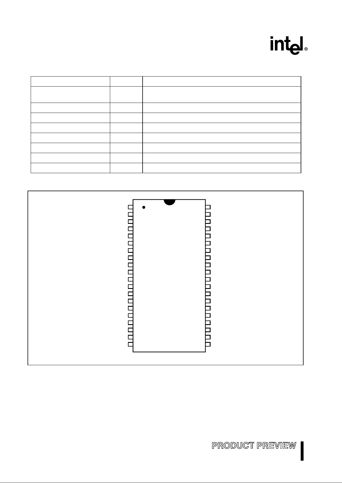
Figure 2. 83C51KB 40-pin DIP Diagram
Table 2. 83C51KB Nomenclature Definitions
Parameter Options Description
Temperature and Burn-in
Options
no mark Commercial operating temperature range (0°C to 70°C) with
Intel standard burn-in.
Packaging Options P Plastic Dual-in-line Package (PDIP)
Program Memory Options 3 F act ory progra mm ed ROM
Process Information C CHMOS
Product Family 51 MCS 51 Compatible Product Family
Device Memory Options KB 128 bytes RAM
4 Kbytes ROM
Device Speed no mark 4-6 MHz
1
2
3
4
5
6
7
8
9
10
11
12
13
14
15
16
17
18
19
20
40
39
38
37
36
35
34
33
32
31
30
29
28
27
26
25
24
23
22
21
P83C51KB
View of
component
as mounted
on PC board
A4248-01
P1.0/KSI0
P1.1/KSI1
P1.2/KSI2
P1.3/KSI3
P1.4/KSI4
P1.5/KSI5
P1.6/KSI6
P1.7/KSI7
RST
P3.0/DATA
P3.1
P3.2/CLK0/INT0#
P3.3/CLK1/INT1#
P3.4/LED0/T0
P3.5/LED1
P3.6/LED2/WR#
P3.7/LED3/RD#
NC
RCIN
V
SS
VCC
P0.0/KSO0/AD0
P0.1/KSO1/AD1
P0.2/KSO2/AD2
P0.3/KSO3/AD3
P0.4/KSO4/AD4
P0.5/KSO5/AD5
P0.6/KSO6/AD6
P0.7/KSO7/AD7
EA#
ALE
PSEN#
P2.7/KSO15/A15
P2.6/KSO14/A14
P2.5/KSO13/A13
P2.4/KSO12/A12
P2.3/KSO11/A11
P2.2/KSO10/A10
P2.1/KSO9/A9
P2.0/KSO8/A8
Page 5
5
83C51KB HIGH PERFORMANCE KEYBOARD MICROCONTROLLER
4.0 83C51KB MEMORY
Table 3. 83C51KB Memory Map
Code
Memory
Description Notes
FFFFH
0000H
External code memory
4
0FFFH
0000H
4-Kbyte on-chip code memory array.
Data
Memory
Description
FFFFH
0000H
External data memory
2, 3
00FFH
0080H
Special function registers
1
007FH
0020H
On-chip RAM
5
001FH
0000H
4 banks of general purpose registers, R0-R7
NOTE:
1. The special function registers (SFRs) are accessible by direct addressing only.
2. Data in this area is accessible by indirect addressing only.
3. RD#/WR# active for these external data addresses.
4. PSEN# active for the external code addresses.
5. Addresses 20H through 2FH are bit addressable.
Page 6
6
83C51KB HIGH PERFORMANCE KEYBO ARD M ICRO CO NT RO L LE R
5.0 SIGNAL DESCRIPTION
Table 4. 40-pin DIP Signals Arranged by Name
Keyboard Keyboard
Name Pin Name Pin
P0.7/KSO7/AD7 32 P 1.0/KSI0 1
P0.6/KSO6/AD6 33 P1.1/KSI1 2
P0.5/KSO5/AD5 34 P1.2/KSI2 3
P0.4/KSO4/AD4 35 P1.3/KSI3 4
P0.3/KSO3/AD3 36 P1.4/KSI4 5
P0.2/KSO2/AD2 37 P1.5/KSI5 6
P0.1/KSO1/AD1 38 P1.6/KSI6 7
P0.0/KSO0/AD0 39 P1.7/KSI7 8
P2.7/KSO15/A15 28 P3.0/DATA 10
P2.6/KSO14/A14 27 P3.1 11
P2.5/KSO13/A13 26 P3.2/CLK0/INT0# 12
P2.4/KSO12/A12 25 P3.3/CLK1/INT1# 13
P2.3/KSO11/A11 24 P3.4/LED0/T0 14
P2.2KSO10/A10 23 P3.5/LED1 15
P2.1/KSO9/A9 22 P3.6/LED2/WR# 16
P2.0/KSO8/A8 21 P3.7/LED3/RD# 17
Chip Control
Name Pin
RCIN 19
RST 9 Power & Ground
ALE 30 Name Pin
PSEN# 29 V
CC
40
EA# 31
V
SS
20
Page 7

7
83C51KB HIGH PERFORMANCE KEYBOARD MICROCONTROLLER
Table 5. 40-pin DIP Signals Arrange d by Pin Numb er
Pin Name Pin Name
1 P 1.0/KSI0 21 P2.0/KSO8/A 8
2 P1.1/KSI1 22 P2.1/KSO9/A 9
3 P1.2/KSI2 23 P2.2KSO10/A10
4 P1.3/KSI3 24 P2.3/KSO11/A 11
5 P1.4/KSI4 25 P2.4/KSO12/A 12
6 P1.5/KSI5 26 P2.5/KSO13/A 13
7 P1.6/KSI6 27 P2.6/KSO14/A 14
8 P1.7/KSI7 28 P2.7/KSO15/A 15
9 RST 29 PSEN#
10 P3.0/DATA 30 ALE
11 P3.1 31 EA#
12 P3.2/CLK0/INT0 # 32 P0.7/KSO 7/A D 7
13 P3.3/CLK1/INT1 # 33 P0.6/KSO 6/A D 6
14 P3.4/LED0/T0 34 P0.5/KS O5/A D 5
15 P3.5/LED1 35 P0.4/KSO4/AD4
16 P3.6/LED2/WR # 36 P0.3/KSO3/A D3
17 P3.7/LED3/RD# 37 P0.2/KSO2/A D2
18 NC 38 P0.1/KSO1/A D1
19 RCIN 39 P0.0/KSO 0/AD 0
20
V
SS
40 V
CC
Page 8

8
83C51KB HIGH PERFORMANCE KEYBO ARD M ICRO CO NT RO LLE R
Table 6. 83C51KB Signal Description
Signal
Name
Type Description
Alternate
Function
A15:8
†
O Address Signals . Upper address lines for the external bus. These
signals are normally used for the KSO15:8 scan function and are not
available for external memory access in a keyboard application. (See
KSO signals).
KSO.15:8
P2.15:8
AD7:0
†
I/O Address/Data Signals. Multiplexed lower address and data signals
for external memory. These signals are normally used for the KSO7:0
scan function and are not available for external memory access in a
keyboard application. (See KSO)
KSO.7:0
P0.7:0
ALE
†
O Address Latch Enable. ALE signals the start of an external bus cycle
and indicates that valid address information is available on lines A15:8
and AD7:0. Since these external address signals are normally used for
the KSO scan function, the ALE should not be used for external memory access in a keyboard application. ALE can be disabled when not
used for external memory access by setting bit 0 of SFR AUX R at
address 8EH.
CLK1:0
P3.3:2
I/O
Clock signal
. Either P3.2 or P3.3 is configurable with a 1.8KΩ pullup
and with external interrupt INT0# or INT1# and used as keyboard CLK
signal.
INT1:0#
DATA
P3.0
I/O
DATA signal
. P3.0 is configurable with a 1.8KΩ pullup and used as keyboard Data signal..
EA# I External Access. Directs program memory accesses to on-chip or off-
chip code memory. For EA# = 0, all program memory accesses are offchip. EA# should always be strapped to V
CC
for keyboard applications
using the 83C51KB.
INT1:0#
†
I External Interrupts 0 and 1. These inputs set bits IE1:0 in the TCON
register. If bits IT1:0 in the TCON register are set, bits IE1:0 are set by
a falling edge on INT1#/INT0#. If bits INT1:0 are clear, bits IE1:0 are
set by a low level on INT1:0#. For keyboard applicaitons, these signals
are normally used for the CLK signals. (See KSIINT and CDPU bits in
the PCON register)
CLK1:0
P3.3:2
KSI7:0
P1.7:0
I/O
Keyboard Scan Inputs
. Application specific keyboard signals.
KSO15:0
P2.15:8
P0.7:0
I/O
Keyboard Scan Outputs
. The KSO signals are application specific to
keyboard scan functions.
LED3:0
P3.7:4
I/O
Light Emitting Diode Drivers
. The LED signals are specifically designed to
drive LEDs connected to Vcc directly (see D.C. Character istics ). The
alternate functions are not available for keyboard applications.
RD#, WR#,
T0
N/C —
No Connection Sign al
. This signal is to be unconnected.
P0.7:0
†
I/O Port 0. This is an 8-bit quasi-bidirectional I/O port (see KSO signals,
see also AD7:0).
AD7:0
P1.7:0 I/O Port 1. This is an 8-bit quasi-bidirectional I/O port (see KSI signals).
P2.7:0 I/O Port 2. This is an 8-bit quasi-bidirectional I/O port (see also A15:8). A15:8
†
The descriptions of RD#, WR#, ALE, P’SEN#, A15:8/P 2.7: 0 and AD7:0/ P0. 7:0 are docum ented for the
standard MCS 51 micr ocont rollers. They are not used for these funct ions in keyboard applications.
Page 9

9
83C51KB HIGH PERFORMANCE KEYBOARD MICROCONTROLLER
P3.7:0 I/O Port 3. This is an 8-bit quasi-bidirectional I/O port (see CLK1:0, DATA,
LED3:0).
PSEN#
†
O Program Store Enable. This output is asserted for external program
memory fetch operations. It is not available for keyboard applications.
—
RCIN I
Resonant Clock Input
. RC resonator generated by connecting 1% precision resistor to VCC or provide an external clock input from an external
clock device.
RD#
†
O Read . Read signal output for external data memory read operations.
It is not available for keyboard applications.
LED3
RST I Reset. Asserting RST when the chip is in idle mode or powerdown
mode returns the chip to normal operation. This signal is input only.
When power is applied to the chip, the internal reset signal remains
high for approximately 80ms to 260ms (see the datasheet for current
specifications). The reset circuit then deactivates and does not reactivate unless V
CC
drops below the crossover at approximately
3VDC.
—
V
CC
PWR Supply Voltage. Connect this pin to the +5V supply voltage. —
V
SS
GND Ci rcui t Gro u n d. Con nect th is pin to ground. —
WR#
†
O Write. Write signal output for external data memory write operations.
It is not available for keyboard applications.
LED2
Table 6. 83C51KB Signal Description
Signal
Name
Type Description
Alternate
Function
†
The descriptions of RD#, WR#, ALE, P’SEN#, A15:8/P2.7:0 and AD7:0/P 0.7: 0 are document ed for the
standard MCS 51 microcontrollers. They are not used for these functions in keyboard applications.
Page 10

10
83C51KB HIGH PERFORMANCE KEYBO ARD M ICRO CO NT RO LLE R
6.0 ELECTRICAL CHARACTERISTICS
ABSOLUTE MAXIMUM RATINGS
†
Ambient Temperature under Bias:
Commercial................................. ..... 0°C to +70°C
Storage Temperature............................. -65°C to +150°C
Voltage on Any Pin to V
SS
...................... -0.5 V to +6.5 V
I
OL
per I/O Pin..........................................................15 mA
Power Dissipation................................................... 1.5 W
NOTE:
Maximum power dissipation is based on
package heat-transfer limitations, not
device power consumption.
OPERATING CONDITIONS
†
TA (Ambient Temperature Under Bias):
Commercial ..................................... 0°C to +70°C
V
CC
(Digital Supply Voltage) ..................... 4.5 V to 5.5 V
V
SS
.................... ...... ..... .......................... .................... 0 V
NOTICE: This document contains informat ion on
products in the design phase of development. Do
not finalize a design with this information. Revised
information will be published when the product is
available. Verify with your local Intel sales office
that you have the latest datasheet before finalizing
a design.
†
WARNING:
Stressing the device beyond the “Absolute Maximum Ratings” may cause permanent damage. These are
stress ratings only. Operation beyond the “Operating Conditions” is not recommended and extended exposure beyond
the “Operating Conditions” may affect device reliability.
Page 11

11
83C51KB HIGH PERFORMANCE KEYBOARD MICROCONTROLLER
Figure 3. RCIN Frequency
NOTE:
RC resonator accuracy is ± 5% at fixed VCC and temperature using a 1% external precision resistor.
7
6.5
6
5.5
5
4.5
4
3.5
3
5678910
RCIN Frequency (MHz)
A4250-01
RCIN Frequency vs. Resistance
Resistance (KOhm)
Page 12

12
83C51KB HIGH PERFORMANCE KEYBO ARD M ICRO CO NT RO LLE R
Figure 4. RC Oscillator
A4245-01
V
CC
V
CC
C
B
A
RCin
external internal
2/3 V
CC
1/3 V
CC
R
Page 13

13
83C51KB HIGH PERFORMANCE KEYBOARD MICROCONTROLLER
6.1 D.C. Characteristics
Table 7. D.C. Characterist ics
Symbol Parameter Min
Typical
(note 1)
Max Unit
Test
Condition
V
IL
Input Low Voltage (except
EA#, RCIN, RST)
-0.5 0.2 V
CC
-0.1 V
V
IL1
Input Low Voltage RST 0 0.2 VCC -0.3 V
V
IL2
Input Low Voltage EA# -0.5 0.5 V
V
IL3
Input Low Voltage RCIN VCC/3 V
V
IH
Input High Voltage (except
EA#, RCIN, RST)
0.2VCC+
0.9
V
CC
+0.5 V
V
IH1
Input High Voltage (EA#,
RST)
0.7V
CC
VCC+0.5 V
V
IH2
Input High Voltage RCIN 2VCC/3 IIH = 8 mA
when external
clock source is
used on RCIN
V
OL
Output Low Voltage (Port 0, 1,
2, 3, ALE, PSEN# except
P3.4/LED0, P3.5/LED1,
P3.6/LED2, P3.7/LED3)
0.3
0.45
1.0
VIOL=200 µA
I
OL
=3.2 mA
IOL=7.0 mA
(note 2,3)
I
OL
Output Low Current
(P3.4/LED0, P3.5/LE D1,
P3.6/LED2, P3.7/LED3 only)
613 22mAV
OL
=3.0 V
V
OH
Output High Voltage (Port 0,
1, 2, 3, ALE, PSEN#, except
P3.0, P3.2, P3.3)
VCC-0.3
VCC-0.7
V
CC
-1.5
VI
OH
= -25 µA
IOH= -65 µA
I
OH
= -100 µA
(note 4)
NOTE:
1. Typical values are obtained using VCC=5.0V, TA=25°C and are not guaranteed.
2. Under steady state (non-transient) conditions, I
OL
must be externally limited as follow:
Maximum I
OL
per Port Pin—Port 0, 1, 2, P3.1-P3.3: 10mA
Maximum I
OL
per Port Pin—P3.4-P3.7: 22mA
Maximum I
OL
per 8-bit port—Port 0-2: 15mA
Ports 3: 95mA
Maximum Total I
OL
for AllOutput Pins: 110mA
If I
OL
exceeds the test conditions, VOL may exceed the related specification. Pins are not guarant eed
to sink current greater than the listed test conditions.
3. Capacitive loading on Ports 0 and 2 may cause spurious noise pulses above 0.4V to be superimposed
on the low level outputs of ALE and Ports 1, 2 and 3. The noise is due to external bus capacitance discharging into the Port 0 and Port 2 pins when these pins change from 1 to 0. In applications where
capacitive loading exceeds 100pF, the noise pulses on these signals may exceed 0.8V. It may be
desirable to qualify signals with a Schmitt Trigger, or CMOS-level input logic.
4. Capacitive loading on Ports 0 and 2 cause the VOH on ALE and PSEN to drop below the 0.9 VCC
specification when the address lines are stabilizing.
Page 14

14
83C51KB HIGH PERFORMANCE KEYBO ARD M ICRO CO NT RO LLE R
V
OH1
Output High Voltage (P3.0,
P3.2, P3.3 without 1.8K Ohm
pullup)
V
CC
-0.3
V
CC
-0.7
VCC-1.5
VI
OH
= -8 µA
I
OH
= -25 µA
IOH= -50 µA
V
OH2
Output High Voltage (P3.0,
P3.2, P3.3 with 1.8K Ohm pullup)
VCC-0.3
V
CC
-0.7
VCC-1.5
VI
OH
= -0.15 mA
I
OH
= -0.50 mA
IOH= -1.0 mA
R
RST
Reset Pulldown Resistor 40 225 K Ohm
R
CD
Pull Up Resistance (P3.0,
P3.2, P3.3 with 1.8K Ohm pullup)
1.2 1.8 2.9 K Ohm
C
IO
Pin Capacitance 10 pF @1MHz, 25°C
I
IL
Logical 0 Input Current (Port
0, 1, 2, 3, except P3.0, P3.2,
P3.3)
-50 µA VIN=0.45V
I
IL1
Logical 0 Input Current (P3.0,
P3.2, P3.3 without 1.8K Ohm
pullup)
-250 µA VIN=0.45V
I
IL2
Logical 0 Input Current (P3.0,
P3.2, P3.2 with 1.8K Ohm pullup)
-1.5 -4.5 mA VIN=0.45V
I
TL
Logical 1-to-0 Transiton Current (Port 0, 1, 2, 3)
-650 µA VIN=2.0V
I
TL1
Logical 1-to-0 Transition Current (P3.0, P3.2 or P3.3 with
1.8K Ohm pullups)
-4.5 mA VIN = 2.0V
Table 7. D.C. Characteristics (Continued)
Symbol Parameter Min
Typical
(note 1)
Max Unit
Test
Condition
NOTE:
1. Typical values are obtained using VCC=5.0V, TA=25°C and are not guaranteed.
2. Under steady state (non-transient) conditions, I
OL
must be externally limited as follow:
Maximum I
OL
per Port Pin—Port 0, 1, 2, P3.1-P 3.3: 10mA
Maximum I
OL
per Port Pin—P3.4-P3.7: 22mA
Maximum I
OL
per 8-bit port—Port 0-2: 15mA
Ports 3: 95mA
Maximum Total I
OL
for AllOutput Pins: 110mA
If I
OL
exceeds the test conditions, VOL may exceed the related specification. Pins are not guaranteed
to sink current greater than the listed test conditions.
3. Capacitive loading on Ports 0 and 2 may cause spurious noise pulses above 0.4V to be superimposed
on the low level outputs of ALE and Ports 1, 2 and 3. The noise is due to external bus capacitance discharging into the Port 0 and Port 2 pins when these pins change from 1 to 0. In applications where
capacitive loading exceeds 100pF, the noise pulses on these signals may exceed 0.8V. It may be
desirable to qualify signals with a Schmitt Trigger, or CMOS-level input logic.
4. Capacitive loading on Ports 0 and 2 cause the V
OH
on ALE and PSEN to drop below the 0.9 VCC
specification when the address lines are stabilizing.
Page 15

15
83C51KB HIGH PERFORMANCE KEYBOARD MICROCONTROLLER
Figure 5. External Clock Drive
I
CC
Power Supply Current:
Active Mode at 6MHz
Idle Mode at 6MHz
Power Down Mode
7
2
10
12
5
50
mA
mA
µA
RST, EA# to
V
CC
RST, EA# to
V
SS
RST, EA# to
V
SS
(RCIN pin to
external resistor, all other
pins are no
connect)
V
POR
Power on reset crossover 2.4 3 3.6 V
Table 7. D.C. Characteristi cs (Continued)
Symbol Parameter Min
Typical
(note 1)
Max Unit
Test
Condition
NOTE:
1. Typical values are obtained using VCC=5.0V, TA=25°C and are not guaranteed.
2. Under steady state (non-transient) conditions, I
OL
must be externally limited as follow:
Maximum I
OL
per Port Pin—Port 0, 1, 2, P3.1-P3.3: 10mA
Maximum I
OL
per Port Pin—P3.4-P3.7: 22mA
Maximum I
OL
per 8-bit port—Port 0-2: 15mA
Ports 3: 95mA
Maximum Total I
OL
for AllOutput Pins: 110mA
If I
OL
exceeds the test conditions, VOL may exceed the related specification. Pins are not guarant eed
to sink current greater than the listed test conditions.
3. Capacitive loading on Ports 0 and 2 may cause spurious noise pulses above 0.4V to be superimposed
on the low level outputs of ALE and Ports 1, 2 and 3. The noise is due to external bus capacitance discharging into the Port 0 and Port 2 pins when these pins change from 1 to 0. In applications where
capacitive loading exceeds 100pF, the noise pulses on these signals may exceed 0.8V. It may be
desirable to qualify signals with a Schmitt Trigger, or CMOS-level input logic.
4. Capacitive loading on Ports 0 and 2 cause the V
OH
on ALE and PSEN to drop below the 0.9 VCC
specification when the address lines are stabilizing.
0.7 VCC
A4252-01
0.45 V
VCC – 0.5
0.2 V
CC
– 0.1
T
CHCL
T
CLCX
T
CLCL
T
CLCH
T
CHCX
Page 16

16
83C51KB HIGH PERFORMANCE KEYBO ARD M ICRO CO NT RO LLE R
6.2 A.C. Characteristics
Table 8. A.C. Characteristics (Note 1, 2)
Symbol Parameter Min Max Unit
F
OSC
RCIN Frequency 4 6 MHz
T
OSC
1/Fosc 166.7 250 ns
T
LHLL
ALE Pulse Width 2Tosc - 50 ·ns
T
AVLL
Address Valid to ALE Low Tosc - 50 ·ns
T
LLAX
Address Hold after ALE Low Tosc - 40 ·ns
T
LLIV
ALE Low to Valid Instruction In 4Tosc - 80 ns
T
LLPL
ALE Low to PSEN# Low Tosc - 40 ns
T
PLPH
Psen# Pulse Width 3Tosc - 60 ns
T
PLIV
Psen# Low to Valid Instruction In 3Tosc - 90 ns
T
PXIX
Input Instruction Hold after PSEN# 0
ns
T
PXIZ
Input Instruction Float after PSEN# Tosc - 20
ns
T
AVIV
Address Valid to Valid Instruction In 5Tosc - 90
ns
T
PLAZ
Psen# Low to Address Float 20
ns
T
RLRH
RD# Pulse Width 6Tosc - 120
ns
T
WLWH
Write# Pulse Width 6Tosc - 120
ns
T
RLDV
RD# Low to Valid Data In 5Tosc - 150
ns
T
RHDX
Input Data Hold after RD# High 0
ns
T
RHDZ
Input Data Float after RD# High 2Tosc - 45
ns
T
LLDV
ALE Low to Valid Data In 8Tosc - 130
ns
T
AVDV
Address Valid to Valid Data In 9Tosc - 145
ns
T
LLWL
ALE Low to RD# or WR# Low 3Tosc - 70 3Tos c + 70
ns
T
AVWL
Address Valid to WR# Low 4Tosc - 150
ns
T
QVWX
Output Data Valid before WR# Tosc - 70
ns
T
QVWH
Output Data Valid to WR# High 7Tosc - 170
ns
T
WHQX
Output Data Hold after WR# High Tosc - 60
ns
T
RLAZ
RD# Low to Address Float 0
ns
T
WHLH
RD# or WR# High to ALE High Tosc - 55 Tosc + 40
ns
T
POR
Power on reset internal high time (note 3) 80 260 ms
NOTE:
1. Capacitive loading=100pF
2. Rise time and fall time = 20ns for external clock drive
3. T
POR
timing begins when the voltage exceeds the V
POR
crossover voltage.
Page 17

17
83C51KB HIGH PERFORMANCE KEYBOARD MICROCONTROLLER
6.3 External Program Memory Read Cycle Waveform
6.4
External Program Memory Read Cycle External Data Memory Read Cycle Waveform
ALE
PSEN#
T
LLAX
T
LHLL
T
AVIV
T
PXIZ
PORT 0
A8 - A15
PORT 2
A8 - A15
A0 - A7 A0 - A7
Instruction In
T
LLIV
T
PLIV
T
LLPL
T
AVLL
T
PLPH
T
PXIX
T
PLAZ
A4254-01
A4255-01
ALE
PSEN#
T
LLAX
T
LHLL
T
AVDV
T
RHDZ
PORT 0
P2.0 - P2.7 or A8 - A15 from DPH
PORT 2
A8 - A15 from PCH
A0-A7 from RI or DPL
A0 - A7 from PCL
Data In
T
WHLH
RD#
T
RHDX
T
AVWL
Instr. In
T
RLDV
T
AVLL
T
LLWL
T
LLDV
T
RLRH
T
RLAZ
Page 18

18
83C51KB HIGH PERFORMANCE KEYBO ARD M ICRO CO NT RO LLE R
6.5 External Data Memory Read Cycle External Data Memory Write Cycle Waveform
Figure 6. External Data Memory Write Cycle
6.6 Testing Characteristics
Figure 7. Float Wavefo rms
A4256-01
ALE
PSEN#
T
LLAX
T
LHLL
T
WHQX
PORT 0
P2.0 - P2.7 or A8 - A15 from DPH
PORT 2
A8 - A15 from PCH
A0-A7 from RI or DPL A0 - A7 from PCL
Data Out
T
WHLH
WR#
T
QVWH
T
AVWL
Instr. In
T
QVWX
T
AVLL
T
LLWL
T
RLWH
V
LOAD
+ 0.1 V
V
LOAD
– 0.1 V
Timing Reference
Points
V
LOAD
V
OH
– 0.1 V
V
OL
+ 0.1 V
For timing purposes, a port pin is no longer floating when a
100 mV change from load voltage occurs and begins to float
when a 100 mV change from the loading V
OH/VOL
level occurs
with I
OL
/
I
OH
= ± 20 mA.
A4243-01
Page 19

19
83C51KB HIGH PERFORMANCE KEYBOARD MICROCONTROLLER
6.7 A.C. Testing Input, Output Waveforms Signature Byte Information
Valid signature bytes for the 83C51KB are detailed in the following table:
Table 9. 83C51K B Signatu re Byte Values
TROM Address Contents Device Type
30H 89H Intel Corp.
31H 58H FX-core
60H 20H 83C51KB
AC inputs during testing are driven at V
CC
– 0.5V for a logic 1
and 0.45 V for a logic 0. Timing measurements are made at
0.45 V
Inputs
Outputs
A4244-01
V
IH
MIN
V
OL
MAX
V
CC
– 0.5
0.2 V
CC
+ 0.9
0.2 V
CC
– 0.1
a min of V
IH
for a logic 1 and V
OL
for a logic 0.
 Loading...