

PRODUCT PREVIEW
80960JD
3.3 V EMBEDDED 32-BIT MICROPROCESSOR
• 3.3 V, 5 V Tolerant, Version of the 80960JD Processor
■ Pin/Code Compatible with all 80960Jx
Processors
■ High-Performance Embedded Architecture
— One Instruction/Clock Execution
— Core Clock Rate is 2x the Bus Clock
— Load/Store Programming Model
— Sixteen 32-Bit Global Registers
— Sixteen 32-Bit Local Registers (8 sets)
— Nine Addressing Modes
— User/Supervisor Protection Model
■ Two-Way Set Associative Instruction Cache
— 80960JD - 4 Kbyte
— Programmable Cache Locking
Mechanism
■ Direct Mapped Data Cache
— 80960JD - 2 Kbyte
— Write Through Operation
■ On-Chip Stack Frame Cache
— Seven Register Sets Can Be Saved
— Automatic Allocation on Call/Return
— 0-7 Frames Reserved for High-Priority
Interrupts
■ On-Chip Data RAM
— 1 Kbyte Critical Variable Storage
— Single-Cycle Access
■ 3.3 V Supply Voltage
— 5 V Tolerant Inputs
— TTL Compatible Outputs
■ High Bandwidth Burst Bus
— 32-Bit Multiplexed Address/Data
— Programmable Memory Configuration
— Selectable 8-, 16-, 32-Bit Bus Widths
— Supports Unaligned Accesses
— Big or Little Endian Byte Ordering
■ High-Speed Interrupt Controller
— 31 Programmable Priorities
— Eight Maskabl e Pins pl u s NMI
— Up to 240 Vectors in Expanded Mode
■ Two On-Chip Timers
— Independe nt 32-B i t Count i ng
— Clock Prescaling by 1, 2, 4 or 8
— lnternal Interrupt Sources
■ Halt Mode for Low Power
■ IEEE 1149.1 (JTAG) Boundary Scan
Compatibility
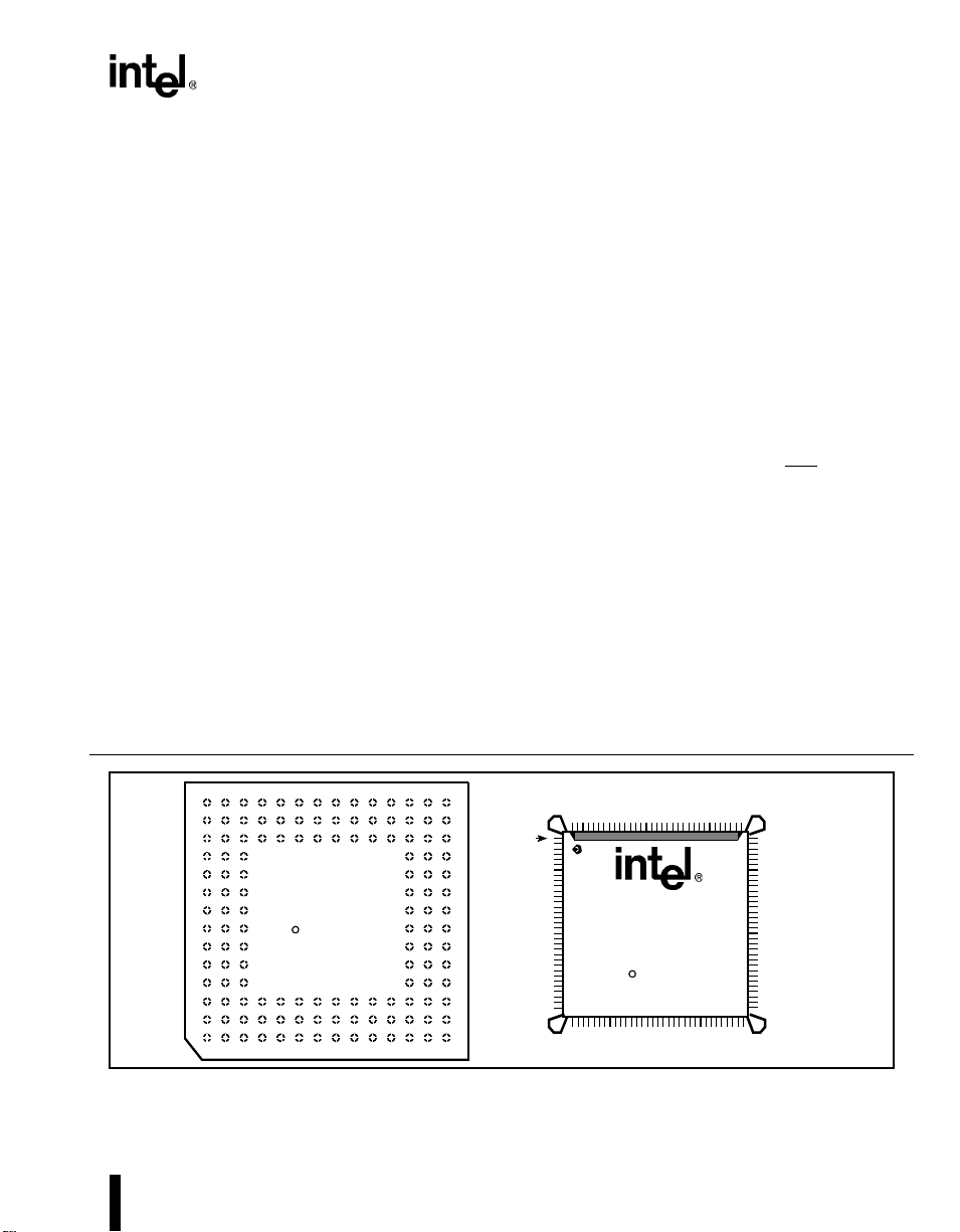
■ Packages
— 132-Lead Pin Grid Array (PGA)
— 132-Lead Plastic Quad Flat Pack (PQFP)
132
PIN 1
99
A80960JD
XXXXXXXXC0
M
© 19xx
i
33
Figure 1. 80960JD Microprocessor
© INTEL CORPORATION, 1996 November 1996 Order Number: 272971-001
i960
NG80960J D
XXXXXXXXC0S
M
i
®
©19xx
66

Information in this document is provided in connection with Intel products. No license, express or implied, by
estoppel or otherwise, to any intellectual property rights is granted by this document. Except as provided in
Intel’s Terms and Conditions of Sale for such products, Intel assumes no liability whatsoever, and Intel
disclaims any express or implied warranty, relating to sale and/or use of Intel products including liability or
warranties relating to fitness for a particular purpose, merchantability, or infringement of any patent, copyright
or other intellectual property right. Intel products are not intended for use in medical, life saving, or life
sustaining applications.
Intel retai ns the right to make changes to specifications and product des criptions at any time, without notice.
*Third-party brands and names are t he property of their respective owners.
Copies of documents which have an ordering number and are referenced in this document, or other Intel
literature, may be obtained from:
Intel Corporation
P.O. Box 7641
Mt. Prospect IL 60056-764
or call 1-800-548-4725
©INTEL CORPORATION, 1996

Contents
80960JD
3.3 V EMBEDDED 32-BIT MICROPROCESSOR
1.0 PURPOSE .................................................................................................................................................. 1
2.0 80960JD OVERVIEW ................................................................................................................................ 1
2.1 80960 Processor Core ........................................................................................................................ 2
2.2 Burst Bus ............................................................................................................................................2
2.3 Timer Unit ...........................................................................................................................................3
2.4 Priority Interrupt Controller .................................................................................................................3
2.5 Instruction Set Summary ....................................................................................................................3
2.6 Faults and Debugging ...................... ..................................................................................................3
2.7 Low Power Operation ......................................................................................................................... 3
2.8 Test Features ..................................................................................................................................... 4
2.9 Memory-Mapped Control Registers ....................................................................................................4
2.10 Data Types and Memory Addressing Modes ................................................................................... 4
3.0 PACKAGE INFORMATION .......................................................................................................................6
3.1 Pin Descriptions .................................................................................................................................. 6
3.1.1 Functional Pin Definitions ........................................................................................................6
3.1.2 80960Jx 132-Lead PGA Pinout .............. .................................................................. .............12
3.1.3 80960Jx PQFP Pinout ........................................................................................................... 16
3.2 Package Thermal Specifications ...................................................................................................... 19
3.3 Thermal Management Accessories ..................................................................................................21
4.0 ELECTRICAL SPECIFICATIONS ...........................................................................................................22
4.1 Absolute Maximum Ratings .............................................................................................................. 22
4.2 Operating Conditions ........................................................................................................................22
4.3 Connection Recommendations ........................................................................................................ 22
4.4 V
4.5 VCCPLL Pin Requirements .............................................................................................................. 23
4.6 DC Specifications ............................................................................................................................. 24
4.7 AC Specifications ............................................................................................................................. 26
5.0 BUS FUNCTIONAL WAVEFORMS ........................................................................................................ 37
6.0 DEVICE IDENTIFICATION ......................................................................................................................51
7.0 REVISION HISTORY ............................................................................................................................... 53
Pin Requirements (V
CC5
4.7.1 AC Test Conditions and Derating Curves ..............................................................................29
4.7.2 AC Timing Waveforms ........................................................................................................... 30
) .......... ...... ... ..... ...... ...... ...... ... ..... ...... ...... ..... ...... ... ...... ..... ...... ...... ... .. 23
DIFF
iii

Contents
FIGURES
Figure 1. 80960JD Micro processor ............................................................... ...................... .......... ........... ......i
Figure 2. 80960JD Block Diagram ................................................................................................................2
Figure 3. 132-Lead Pin Grid Array Bottom View - Pins Facing Up .............................................................12
Figure 4. 132-Lead Pin Grid Array Top View - Pins Facing Down ..............................................................13
Figure 5. 132-Lead PQFP - Top View .........................................................................................................16
Figure 6. VCC5 Current-Limiting Resistor ...................................................................................................23
Figure 7. VCCPLL Lowpass Filter ...............................................................................................................23
Figure 8. AC Test Load ...............................................................................................................................29
Figure 9. Output Delay or Hold vs. Load Capacitance ................................................................................29
Figure 10. CLKIN Waveform .........................................................................................................................30
Figure 11. Output D el ay Waveform for T
Figure 12. Out put Float Waveform for T
Figure 13. Input Setup and Hold Wav eform for T
Figure 14. Input Setup and Hold Wav eform for T
Figure 15. Input Setup and Hold Wav eform for T
Figure 16. Input Setup and Hold Wav eform for T
Figure 17. Relat i ve Timings Waveform for T
Figure 18. DT/R and DEN Timings Waveform ..............................................................................................34
Figure 19. TCK Waveform ............................................................................................................................34
Figure 20. Input Setup and Hold Wav eforms for T
Figure 21. Out put Delay and Output Float Waveform for T
Figure 22. Out put Delay and Output Float Waveform for T
Figure 23. Input Setup and Hold Wav eform for T
Figure 24. Non-Burst Read and Write Transactions Without Wait States, 32-Bit Bus ..................................37
Figure 25. Burs t Read and Write Trans actions Without Wait States, 32-Bit Bus .......... ................................38
Figure 26. Burst Write Transactions With 2,1,1,1 Wait States, 32-Bit Bus ...................................................39
Figure 27. Burs t Read and Write Trans actions Without Wait States, 8-Bit Bus ..................... ...................... .40
Figure 28. Burs t Read and Write Trans actions With 1, 0 Wait States
and Extra Tr State on Read, 16-Bit Bus .......................................................................................41
Figure 29. Bus Transactions Generated by Double Word Read Bus Request,
Misaligned One Byte From Quad Word Boundary, 32-Bit Bus, Little Endian ............... ........... ....42
Figure 30. HOLD/HOLDA Waveform For Bus Arbitration .............................................................................43
Figure 31. Cold Reset Waveform ..................................................................................................................44
Figure 32. Warm Reset Waveform ................................................................................................................45
Figure 33. Entering the ONCE State .............................................................................................................46
Figure 34. Summary of Aligned and Unaligned Accesses (32-Bit Bus) ........................................................49
Figure 35. Summary of Aligned and Unaligned Accesses (32-Bit Bus) (Continued) ....................................50
Figure 36. 80960JD Device Identification Register ............................................... ........................................51
................................................................................................30
OV1
...................................................................................................31
OF
and T
IS1
and T
IS2
and T
IS3
and T
IS4
, T
LX
LXL
BSIS1
BSIS2
......................................................................31
IH1
......................................................................32
IH2
......................................................................32
IH3
......................................................................33
IH4
and T
.................................................................... 33
LXA
and T
and T
........... ................. ................. ................ 35
BSIH1
AND T
BSOV1
and T
BSOV2
.......... ........ ......... ........ ......... ......... ........ ..3 6
BSIH2
........... ..... ...... ...... ...... .. ...... ..3 5
BSOF1
............................................. 36
BSOF2
iv

Contents
TABLES
Table 1. 80960Jx Instruction Set ......................... ........... ........... .................................................... ..............5
Table 2. Pin Description Nomenclature ....................................................................................................... 6
Table 3. Pin Description — External Bus Signals ........................................................................................ 7
Table 4. Pin Description — Processor Control Signals, Test Signals and Power .....................................10
Table 5. Pin Description — Interrupt Unit Signals .....................................................................................11
Table 6. 132-Lead PGA Pi nout — In Signal Order ................. .................................................... ...............14
Table 7. 132-Lead PGA Pinout — In Pin Order .......... ........................................................................... ....15
Table 8. 132-Lead PQFP Pinout — In Signal Order .................................................................................. 17
Table 9. 132-Lead PQFP Pinout — In Pin Order ....................................................................................... 18
Table 10. 132-Lead PGA Package Thermal Characteristics ....................................................................... 19
Table 11. 132-Lead PQFP Package Thermal Characteristics .....................................................................20
Table 12. Maximum T
Table 13. 80960JD Operating Conditions ................... .................................................... ...................... .......22
Table 14. 80960JD DC Characteristics .............................. ......................................................... ................24
Table 15. 80960JD ICC Characteristics ......................................................................................................25
Table 16. 80960JD AC Characteristics ........... ......................................... ...................... .......... ........... .........26
Table 17. Note Definitions for Table 16, 80960JD AC Characteristics (pg. 26) ...........................................28
Table 18. Natural Boundaries for Load and Store Accesses ............................ ........... ...................... ..........47
Table 19. Summary of Byte Load and Store Accesses ................................................. .......... ........... .........47
Table 20. Summary of Short Word Load and Store Accesses ......................... ........... ...................... ..........47
Table 21. Summary of n-Word Load and Store Accesses (n = 1, 2, 3, 4) ........... ...................... ..................48
Table 22. 80960JD66 Die and Stepping Reference .............................................. ...................... .......... ......51
Table 23. Fields of 80960JD Device ID ....................................................................................................... 52
Table 24. 80960JD Device ID Model Ty pes ............ ........... .......... ........... ...................... .......... ........... .........52
Table 25. Device ID Version Numbers for Different St eppings .......... ...................... .......... ........... ...............52
at Various Airflows in °C ......................................................................................... 21
A
v


80960JD
1.0 PURPOSE
This document contains preview information for the
80960JD microprocessor, including electrical
characteristics and package pinout information.
Detailed functional descriptions — other than
parametric performance — are published in the
i960® Jx Microprocessor User’s Guide
Throughout this data sheet, references to “80960Jx”
indicate features which appl y to all of the foll owing:
• 80960JA — 5V, 2 Kbyte instruction cach e, 1 Kbyte
data cache
• 80L960JA — 3.3V version of the 80960JA
• 80960JD — 5V, 4 Kbyte instruction ca che, 2Kbyte
data cache and clock doubling
• 80960JD — 3.3V, 5V Tolerant version of the
80960JD
• 80960JF — 5V, 4 Kbyte instruction c ache , 2 Kbyte
data cache
• 80L960JF — 3.3 V version of the 80960JF
(272483).
2.0 80960JD OVERVIEW
The 80960JD offers high performance to costsensitive 32-bit embedded applications. The
80960JD is object code compatible with the 80960
Core Architecture and is capable of sustained
execution at the rate of one instruction per clock.
This processor’s features include generous
instruction cache, data cache and data RAM. It also
boasts a fast interrupt mechanism, dual programmable timer units and new instructions .
The 80960JD’s cloc k doub ler op era tes t he pr ocess or
core at twice the bus clock rate to improve execution
performance without increasing the complexity of
board designs.
Memory subsystems for cost-sensitive embedded
applications often impose substantial wait state
penalties. The 80960JD integrates considerable
storage resources on-chip to decouple CPU
execution from the external bus.
The 80960JD rapidly allocate s and deallocates local
register sets during contex t switches. The processor
needs to flush a register set to the stack only w hen it
saves more than seve n sets to its local register cache.
A 32-bit multiplexed burst bus provides a high-speed
interface to system memory and I/O. A full
complement of control signals simplifies the
connection of the 80960JD to external components.
The user programs physical and logical memory
attributes through memory-mapped control registers
(MMRs) — an extension not found on the i960 Kx,
Sx or Cx processors. Physica l and logical configuration registers enable the processor to operate with
all combinations of bus width and data object
alignment. The processor supports a homogeneous
byte ordering model.
This processor integrates two important peripherals:
a timer unit and an interrupt controller. These and
other hardware resources are programmed through
memory-mapped control registers, an extension to
the familiar 80960 architecture.
The timer unit (TU) offers two independent 32-bit
timers for use as real-time system clocks and
general-purpose system timing. These operate in
either single-shot or auto-reload mode and can
generate interrupts.
The interrupt controller unit (ICU) provides a flexible
means for requesting interrupts. The ICU provides
full programmability of up to 240 interrupt sources
into 31 priority levels. The ICU takes advantage of a
cached priority table and optional routine caching to
minimize interrupt latency. Clock doubling reduces
interrupt latency by 40% compared to the
80960JA/JF. Local registers may be dedicated to
high-priority interrupts to further reduce latency.
Acting independently from the core, the ICU
compares the priorities of posted interrupts with the
current process priori ty, off-loading this task from the
core. The ICU also supports the integrated timer
interrupts.
The 80960JD features a Halt mode designed to
support applications where low power consumption
is critical. The halt instruction shuts down instruction
execution, resulting in a power savings of up to 90
percent.
The 80960JD’s testability features, including ONCE
(On-Circuit Emulation) mode and Boundary Scan
(JTAG), provide a powerful environment for design
debug and fault di agnosis.
The
Solutions9 60®
of development tools which support the i960
processor family. Many of these tools are developed
by partner companies; some are developed by Intel,
such as profile-driven optimizing compilers. For
more information on these products, contact your
local Intel representative.
program features a wide variety
PRODUCT PREVI EW 1
80960JD
CLKIN
TAP
Local Register Cache
PLL, Clocks,
Power Mgmt
Boundary Scan
5
8-Set
128
Global / Local
Register File
SRC2 DESTSRC1
Controller
3 Independent 32-Bit SRC1, SRC2, and DEST Buses
4 K Byte Instruction Cache
Two-Way Se t Associative
Constants
and
Address
Unit
effective
address
SRC1
SRC2
Control
DEST
Multiply
Divide
Unit
SRC1
SRC2
Instruction Sequencer
Execution
Generation
DEST
Figure 2. 80960JD Block Diagram
Memory
Interface
Unit
32-bit Address
32-bit Data
SRC1
32-bit buses
address / data
DEST
Physical R egion
Configuration
Bus
Control Unit
Bus Request
Queues
Two 32-Bit
Timers
Programmable
Interrupt Controller
Memory-Mapped
Register Interface
1K byte
Data RAM
2 Kbyte Direct
Mapped Data
Cache
Control
21
Address/
Data Bus
32
Interrupt
Port
9
2.1 80960 Processor Core
The 80960Jx family is a sca l ar implementation of the
80960 Core Architecture. Intel designed this
processor core as a very high performance device
that is also cost-effec tive. Factors that contribute to
the core’s performance include:
• Core operates at twic e the bus speed (80960J D
only)
• Single-clock execution of most instructi ons
• Independent Multi ply/Divide Unit
• Efficient instruction pipeli ne mi nimizes pipelin e
break latency
• Register and resource sc oreboarding allow
overlapped instruction execution
• 128-bit register bus speeds local regi st er caching
• 4 Kbyte two-way set associative, integrated
instruction cache
2
• 2 Kbyte direct-mapped, integrated data c ache
• 1 Kbyte integrated data RAM delivers zero wait
state program data
2.2 Burst Bus
A 32-bit high-performance bus controller interfaces
the 80960JD to external memory and peripherals.
The BCU fetches instructions and transfers data at
the rate of up to four 32-bit words per six clock
cycles. The external address/data bus is multiplexed.
Users may configure the 80960JD’s bus controller to
match an application’s fundamental memory organization. Physical bus width is register-programmed
for up to eight regions. Byte ordering and data
caching are programmed through a group of logical
memory templates and a defaults regist er.
PRODUCT PREVIEW

80960JD
The BCU’s features include:
• Multiplexed external bus to minimize pin count
• 32-, 16- and 8-bit bus wi dths to simplify I/O
interfaces
• External ready control for address-to-data, data-todata and data-to-next-addres s wai t state types
• Support for big or lit tle endian byte ordering to
facilitate the porting of existing program code
• Unaligned bus accesses performed transparently
• Three-deep load/store queue to decouple the bus
from the core
Upon reset, the 80960JD conducts an internal self
test. Then, before executing its first instruction, it
performs an external bus confidence test by
performing a checksum on the first words of the
initialization boot record (IBR).
The user may examine the contents of the caches at
any time by executing special cache control instructions.
2.3 Timer Unit
The timer unit (TU) contains two independent 32-bit
timers which are capable of coun tin g at s evera l clo ck
rates and gener at ing in te rrup ts. Each is pr ogrammed
by use of the TU registers. These memory-mapped
registers are addressable on 32-bit boundaries. The
timers have a single-shot mode and auto-reload
capabilities for continuous operation. Each timer has
an independent interrupt request to the 80960JD’s
interrupt controller. The TU can generate a fault
when unauthorized writes from user mode are
detected. Clock prescaling is su pported.
• Interrupt vectors and interr upt han dler rou tines can
be reserved on-chip
• Register frames for high-priority interrupt handl ers
can be cached on-chi p
• The interrupt stack can be placed in cacheable
memory space
• Interrupt microcode executes at twice the bus
frequency
2.5 Instruction Set Summary
The 80960Jx adds several new instructions to the
i960 core archi tecture. The new ins tructions are:
• Conditional Move
• Conditional Add
• Conditional Subtract
•Byte Swap
•Halt
• Cache Control
• Interrupt Control
Table 1 identifies the instructions that the 80960Jx
supports. Refer to
Guide
(272483) for a detailed description of each
instruction.
i960® Jx Microprocessor User’s
2.6 Faults and Debugging
The 80960Jx employs a comprehensive fault model.
The processor responds to faults by making implicit
calls to a fault handling routine. Specific information
collected for each fault allows the fault handler to
diagnose exceptions and recover appropriately.
2.4 Priority Interrupt Controller
A programmable interrupt controller manages up to
240 external sources through an 8-bit external
interrupt port. Alternatively, the interrupt inputs may
be configured for individual edge- or level-triggered
inputs. The interrupt unit (IU) also accepts interrupts
from the two on-chip timer channels and a single
Non-Maskable Interrupt (NMI
servic ed accordin g to their prio rity levels rel ative to
the current proce ss pri ority.
Low interrupt latency is critical to many embedded
applications. As part of its highly flexible interrupt
mechanism, the 80960JD exploits several
techniques t o mi nimize latency:
) pin. Interrupts are
The processor also has buil t-in debug capabilities. In
software, the 80960Jx may be configured to detect
as many as seven different trace event types. Alternatively, mark and fmark instructions can generate
trace events explicitly in the instruction stream.
Hardware breakpoint registers are also available to
trap on execution and data addresses.
2.7 Low Power Operation
Intel fabricates the 80960Jx using an advanced sub-
micron manufac turing process. The processor’s submicron topology provides the circuit density for
optimal cache size and high operating speeds while
PRODUCT PREVI EW 3

80960JD
dissipating modest power. The processor also uses
dynamic power management to turn off clocks to
unused circuits.
Users may program the 80960Jx to enter Halt mode
for maximum power savings. In Halt mode, the
processor core stops completely while the integrated
peripherals continue to function, reducing overall
power requirements up to 90 percent. Processor
execution resumes from internally or externally
generated int errupts.
2.8 Test Features
The 80960Jx incorporates numerous features which
enhance the user’s ability to test both the processor
and the system to which it is attached. These
features include ONCE (On-Circuit Emulation) mode
and Boundary Sc an (JTAG).
The 80960Jx provides test ability featu r es compatible
with IEEE Standard Test Access Port and Boundary
Scan Architec ture (IEEE Std. 1149.1).
One of the boundary scan instructions, HIGHZ,
forces the processor to float all its output pins
(ONCE mode). ONCE mode can also be initiated at
reset witho ut using the boundary scan mechanism.
ONCE mode is useful for board-level testing. This
feature allows a mounted 80960JD to electrically
“remove” itself from a circuit board. This allows for
system-level testin g where a remote tester — such
as an in-circuit emulator — can exercise the
processor system.
The provided test logic does not interfere with
component or circuit board behavior and ensures
that components function correctly, connections
between various components are correct, and
various components interact correctly on the printed
circuit board.
2.9 Memory-Mapped Control Registers
The 80960JD, though compliant with i960 series
processor core, has the added advantage of
memory-mapped, intern al control registers not found
on the i960 Kx, Sx or Cx processors. These give
software the interface to easily read and modify
internal control registers.
Each of these registers is accessed as a memorymapped, 32-bit register. Access is accomplished
through regular memory-format instructions. The
processor ensures that these accesses do not
generate external bus cycles.
2.10 Data Types and Memory Addressing Modes
As with all i960 family processors, the 80960Jx
instruction set supports several data types and
formats:
•Bit
•Bit fields
• Integer (8-, 16-, 32-, 64-bit)
• Ordinal (8-, 16-, 32-, 64-bit unsigned i ntegers)
• Triple word (96 bits)
• Quad word (128 bits)
The 80960Jx prov ides a ful l set of addre ssin g modes
for C and assembly programming:
• Two Absolute modes
• Fiv e Re gi ster Indir e ct m od e s
• Index with displacement
• IP with displacement
The JTAG Boundary Scan feature is an attractive
alternative to conventional “bed-of-nails” testing. It
can examine connections which might otherwise be
inaccessible to a test system.
4
PRODUCT PREVIEW

80960JD
Table 1. 80960Jx Instruction Set
Data Movement Arithmetic Logical Bit, Bit Field and Byte
Load
Store
Move
*Conditional Select
Load Address
Comparison Branch Call/Ret urn Fault
Compare
Conditional Compare
Compare and
Increment
Compare and
Decrement
Test Condition Code
Check Bit
Debug
Modify Trace Controls
Mark
Force Mark
NOTES: Asterisk (*) denotes new 80960Jx instructions unavailable on 80960CA/CF, 80960KA/KB and 80960SA/SB
implementations.
Add
Subtract
Multiply
Divide
Remainder
Modulo
Shift
Extended Shi ft
Extended Multiply
Extended Divide
Add with Carry
Subtract with Carry
*Conditional Add
*Conditional Subtract
Rotate
Unconditional Branch
Conditional Branch
Compare and Branch
Processor
Management
Flush Local Registers
Modify Arithmetic
Controls
Modify Process
Controls
*Halt
System Control
*Cache Control
*Interrupt Control
And
Not And
And Not
Or
Exclusive Or
Not Or
Or Not
Nor
Exclusive Nor
Not
Nand
Call
Call Extended
Call System
Return
Branch and Link
Atomic
Atomic Add
Atomic Modify
Set Bit
Clear Bit
Not Bit
Alter Bit
Scan For Bit
Span Over Bit
Extract
Modify
Scan Byte for Equal
*Byte Swap
Conditional Fault
Synchronize Faults
PRODUCT PREVI EW 5

80960JD
3.0 PACKAGE INFORMATION
The 80960JD is offered with three speeds and two
package types. The 132-pin Pin Grid Array (PGA)
device is specified for operation at V
over a case temperature range of 0° to 10 0°C :
=3.3V±5%
CC
• A80960JD-66 (66 MHz core, 33 MHz bus)
• A80960JD-50 (50 MHz core, 25 MHz bus)
• A80960JD-40 (40 MHz core, 20 MHz bus)
The 132-pin Plastic Quad Flatpack (PQFP) devices
will be specified for operation at V
over a case temperature range of 0° to 10 0°C :
= 3.3 V ± 5%
CC
• NG80960JD-66 (66 MHz core, 33 MHz bus)
• NG80960JD-50 (50 MHz core, 25 MHz bus)
• NG80960JD-40 (40 MHz core, 20 MHz bus)
For complete package specifications and infor-
mation, refer to Intel’s
Packaging Handbook
(240800).
3.1 Pin Descriptions
This section describes the pins for the 80960JD in
the 132-pin ceramic Pin Grid Array (PGA) package
and 132-lead Plastic Quad Flatpack Package
(PQFP).
Section 3.1.1, Functional Pin Definitions
describes pin function; Section 3.1.2, 80960Jx 132Lead PGA Pinout and Section 3.1.3, 80960Jx
PQFP Pinout define the signal and pin locations for
the supported package types.
3.1.1 Functional Pin Definitions
Table 2 presents the legend for interpreting the pin
descriptions which follow. Pins associa ted with the
bus interface are described in Table 3. Pins
associated with basic control and test functions are
described in Table 4. Pins associated with the
Interrupt Unit are described in Table 5.
Table 2. Pin Description Nomenclature
Symbol Description
I Input pin only.
O Output pin only.
I/O Pin can be either an input or output.
– Pin must be connected as described.
S Synchronous. Inputs must meet setup
and hold times relative to CLKI N for
proper operation .
S(E) Edge sensi tive input
S(L) Level sensitive input
A (...) Asynchronous. Inputs may be
asynchronous relative to CLKIN.
A(E) Edge sensi tive input
A(L) Level sensitive input
R (...) While the processor’s R ESET
pin is
asserted, the pin:
R(1) is driven to V
R(0) is driven to V
R(Q) is a valid output
CC
SS
R(X) is driven to unknown state
R(H) is pulled up to V
CC
H (...) While the processor is in the hold state,
the pin:
H(1) is driven to V
H(0) is driven to V
H(Q) Maintain s previous state or
CC
SS
continues to be a valid output
H(Z) Floats
P (...) While the processor is halted, the pin:
P(1) is driven to V
P(0) is driven to V
P(Q) Maintains previous state or
CC
SS
continues to be a valid output
6
PRODUCT PREVIEW
Table 3. Pin Description — External Bus Signals (Sheet 1 of 4)
NAME TYPE DESCRIPTION
AD31:0 I/O
R(X)
H(Z)
P(Q)
ADDRESS / DATA BUS carries 32-bit physical addresses and 8-, 16- or 32-bit data
to and from memory . D uring an address (
S(L)
address (bits 0- 1 i ndicate SIZE; see below). During a data (T
T
a
data is present on one or more contiguous bytes, comprising AD31:24, AD23:16,
AD15:8 and AD7:0. During write operations, unused pins are driven to determinate
values.
SIZE, which comprises bits 0-1 of th e AD l ines during a
number of data trans fers during the bus transaction.
AD1 AD0 Bus Transfers
0 0 1 Transfer
0 1 2 Transfers
1 0 3 Transfers
1 1 4 Transfers
When the processor enters Halt mode, if the previous bus operation was a:
• write — AD31:2 are driven with the last data value on the AD bus.
• read — AD31:4 are driven wi th the last address va lue on the AD bus; AD3:2 are
driven with the value of A3:2 from the last data cycle.
Typically, AD 1:0 reflect the SIZE information of the last bus transac ti on (either
instruction fetch or load/store) that was execut ed before enteri ng H alt mode.
ALE O
R(0)
H(Z)
ADDRESS LATCH ENABLE indicates the transfer of a physical addres s. ALE is
asserted during a
active HIGH and floats to a high impedance state during a hold cycle (T
T
cycle and deasserted before the beginning of the Td state. It is
a
P(0)
ALE
R(1)
H(Z)
ADDRESS LATCH ENABLE indicates the transfer of a phys ical addres s. ALE
O
inverted ver si on o f ALE . This sign al g iv es t he 80960J D a hig h de gree o f co mpat ibil i ty
with existing 80960Kx systems.
P(1)
ADS
R(1)
H(Z)
ADDRESS STROBE indicates a valid add ress and the start of a new bus access.
O
The processor assert s ADS
samples ADS
at the end of the cycle.
for the entire Ta cycle. Exter nal b us c ontrol logi c t ypic all y
P(1)
A3:2 O
R(X)
H(Z)
P(Q)
ADDRESS3:2 comprise a partial demultiplexed ad dress bus.
32-bit memory accesses:
the processor asse rts address bits A3:2 during Ta. The
partial word address increments with each assertion of RDYRCV
16-bit memory accesses:
driven on the
of RDYRCV
BE1 pin. The par tial short word addres s increme nts wit h each assert ion
during a burst.
8-bit memory accesses:
driven on BE1: 0
RDYRCV
. The partial byte address increments with each assertion of
during a burst.
the processor asse rts address bits A3:1 during Ta with A1
the processor as sert s addr es s bits A3 :0 duri ng Ta, with A1:0
80960JD
) cycle, bits 31:2 contain a physical word
) cycle, read or write
d
T
cycle, specifies the
a
).
h
is the
during a burst.
PRODUCT PREVI EW 7
80960JD
Table 3. Pin Description — External Bus Signals (Sheet 2 of 4)
NAME TYPE DESCRIPTION
BE3:0 O
R(1)
H(Z)
P(1)
BYTE ENABLES select which of up to four data bytes on the bus participate in the
current bus ac cess. Byte enabl e encoding is dependent on the bus width of the
memory region accessed:
32-bit bus:
enables data on AD31:24
BE3
BE2
enables data on AD23:16
BE1
enables data on AD15:8
BE0
enables data on AD7:0
16-bit bus:
BE3 becomes Byte High Enab l e (enables data on AD15:8)
BE2
is not used (state is high)
BE1
becomes Address Bit 1 (A1)
BE0
become s By t e Low Enabl e (e na b l es da t a on AD7:0)
8-bit bus:
BE3 is not used (state is high)
BE2
is not used (state is high)
BE1
becomes Address Bit 1 (A1)
BE0
becomes Address Bit 0 (A0)
The processor ass erts byte ena bles, byt e hig h en able and byt e low e nab le du ring
Since unaligned bus requests are sp lit into separate bus transactions, these signals
do not toggle during a burst. They remai n active through t he l ast T
For accesses to 8- and 16-bit memory, the processor asserts the address bits in
conjunction with A3:2 described above.
WIDTH/
HLTD1:0OR(0)
H(Z)
P(1)
WIDTH/HALTED signals denote the physical memory attribute s for a bus transaction:
WIDTH/HLTD1 WIDTH/HLTD0
00 8 Bits Wide
0 1 16 Bits Wide
1 0 32 Bits Wide
1 1 Processor Hal ted
The processor floats the WIDTH/HLTD pins whenever it rel i nquishes the bus in
response to a HOLD request, regardless of prior operating state.
D/C
R(X)
H(Z)
P(Q)
W/R
R(0)
H(Z)
P(Q)
DT/R
R(0)
H(Z)
P(Q)
DATA/CODE indicates that a bus access is a data access (1) or an instruction
O
access (0). D/C
has the same timi ng as W/R.
0 = instruction access
1 = data access
WRITE/READ specifies, during a
O
read (0). It is l atched on-chip and r emai ns valid during T
T
cycle, whether the operation is a write (1) or
a
0 = read
1 = write
DATA TRANSMIT / RECEIVE indicates the direction of data transfer to and from the
O
address/data bus. It is low during T
and T
/Td cycles for a write. DT/R never changes state when DEN is asserted.
w
and Tw/Td cycles for a read; it is high duri ng Ta
a
0 = receive
1 = transmit
cycles.
d
cycle.
d
T
.
a
8
PRODUCT PREVIEW
Table 3. Pin Description — External Bus Signals (Sheet 3 of 4)
NAME TYPE DESCRIPTION
DEN O
BLAST
RDYRCV
LOCK
ONCE
HOLD I
R(1)
H(Z)
R(1)
H(Z)
/
R(H)
H(Z)
DATA ENABLE indicates data transf er cycles during a bus access. DEN
at the start of the first data cycle in a bus access and deasserted at the end of the
last data cycle. DEN
P(1)
connected to the data bus.
0 = data cycle
1 = not data cycle
BURST LAST indicates the last trans fe r in a bus access. BLA ST
O
last data transfer of burst and non-burst accesses . BLAST
wait states are inserted via the RDYRCV
P(1)
data transfer in a bus cycle.
0 = last dat a tr an sfer
1 = not last data transfer
I
READY/RECOVER indicates that data on AD lines can be sampled or removed. If
S(L)
RDYRCV
by inserting a wa it state (T
0 = sample data
1 = don’t sample data
The RDYRCV
continues to insert additional recovery st ates until it sampl es the pin HIGH. T hi s
function gives slow external devi ces more time to float their buffers before the
processor beg i ns to drive address ag ain.
0 = insert wait states
1 = recovery complete
BUS LOCK indicates that an atomic read-modify-write operation is in progress. The
I/O
LOCK
S(L)
the last data transfer of the sequence. The processor does not grant HOLDA while it
is asserting LOCK
P(1)
in semaphore operations.
0 = Atomic read-modify-write in progress
1 = Atomic read-modify-write not in progress
ONCE MODE: The processor samples the ONCE
LOW at the end of reset, the processor enters ONCE mode. In ONCE mode, the
processor stops all clocks and floats all output pins. The pin has a weak internal
pullup which is active during reset to ensure normal operation when the pin is l eft
unconnected.
0 = ONCE mode enabled
1 = ONCE mode not enabled
HOLD: A request from an ext ernal bus master to acq uire the bus. When the
S(L)
processor receiv es HOLD and grants bus control to another master, i t as serts
HOLDA, floats the address/d ata and control lines and enters the T
HOLD is deasserted, the processor deasserts HOLDA and enters either the T
state, resuming control of the address/data and control lines.
0 = no hold request
1 = hold request
is not asserte d du ring a Td cycle, th e Td cycle is extended to the next cycle
output is asserted in the first cl ock of an atomic operation and deasserted in
is used with DT/R to provide control for data transceivers
pin. BLAST become s in acti ve afte r th e f inal
).
w
pin has another func ti on duri ng th e recov ery (Tr) state. The processor
. This prevents external agents from accessing memory i nvolved
80960JD
is asserted
is asserted in the
remains active as long as
input during r eset. If it is asserted
state. When
h
or Ta
i
PRODUCT PREVI EW 9
80960JD
Table 3. Pin Description — External Bus Signals (Sheet 4 of 4)
NAME TYPE DESCRIPTION
HOLDA O
R(Q)
H(1)
P(Q)
BSTAT O
R(0)
H(Q)
P(0)
Table 4. Pin Description — Processor C ontrol Signals, Test Signals and Power (Sheet 1 of 2)
NAME TYPE DESCRIPTION
CLKIN I CLOCK INPUT provides the processor’s fundamental time base; bot h the processor
RESET
A(L)
STEST I
S(L)
FAIL
R(0)
H(Q)
P(1)
TCK I TEST CLOCK is a CPU input which provides the clocking function for IEEE 1149.1
TDI I
S(L)
HOLD ACKNOWLEDGE indicates to an external bus master that the processor has
relinquished control of the bus. T he processor can grant HOLD requests and enter
the T
state during reset and while halted as well as during regular operat i on.
h
0 = hold not acknowledged
1 = hold acknowledged
BUS STATUS indicates that th e processor may soon stall unless it has suffi cient
access to the bus; see
logic can examine this signal to determine when an external bus master should
acquire/relinquish the bus.
0 = no potential st all
1 = potential stall
core and the external bus run at the CLKIN rate. All input and output timings are
specified rel ative to a rising CLKIN edge.
I
RESET initializes the processor and clears its internal logic. During reset, the
processor places the address/data bus and control output pins in their idle (inactive)
states.
During reset, the input pins are ignored with the exception of LOCK
and HOLD.
The RESET
ization during po w e r up , RE SET
cycles with V
a minimum of 15 cycles.
SELF TEST enables or disables the processor’s i nternal self-te st feature at init i alization. STE ST is examined at the end of reset. When STEST is asserted, the
processor performs its internal self-test and t he external bus conf i dence test. When
STEST is deasserted, the processor performs only the ex ternal bus confidence test.
0 = self test disabled
1 = self test enabl ed
FAIL indicates a failure of the processor’s built-in self-tes t performed during ini tial-
O
ization. FAIL
indicate the status of indiv idual tests:
• When self-test passes, the processor deass erts FAIL
user code.
• When self-test fails, the processor asserts FAIL
0 = self test failed
1 = self test passed
Boundary Scan Tes ting (JTAG). State i nformation and data are clocked into the
processor on the ris ing edg e; data is cl ocked out of the pro cesso r on the f alling edge .
TEST DATA INPUT is the serial input pin for JTAG. TDI is sampled on the rising
edge of TCK, during the SHIFT-IR and SHIFT-DR states of the T est Access Port.
pin has an internal synchro nizer . To ens ure pred ictab le pro cesso r ini tial -
CC
is asserted immediately upon reset and toggles during self-test to
i960® Jx Microprocessor User’s Guide
must be asserted a mini mum of 10,000 CLKIN
and CLKIN stable. On a warm reset, RESET should be asserted for
and then stops executing.
(272483). Arbitration
/ONCE, STEST
and begins opera tion from
10
PRODUCT PREVIEW
Table 4. Pin Description — Processor C ontrol Signals, Test Signals and Power (Sheet 2 of 2)
NAME TYPE DESCRIPTION
TDO O
R(Q)
TEST DATA OUTPUT is the serial output pin for JTAG. TDO is driven on the falling
edge of TCK during the SHIFT-IR and SH IFT-DR states of the Test Access Port. At
other times, TDO fl oats. TDO does not float during ONCE mode.
HQ)
P(Q)
TRST
TMS I
V
CC
V
CCPLL
I
TEST RESET asynchronously resets the Test Access Port (TAP) c ontroller functi on
A(L)
of IEEE 1149.1 Boundary Scan testing (JTAG). When u sing the Boundary Scan
feature, conn ect a pulldown resistor between this pin and V
this pin must be conne cted to V
Connection Recommendations (pg. 22).
; however, no re si stor is r equi red. Se e Se ction 4. 3,
SS
. If TAP is not used,
SS
TEST MODE SELECT is sampled at the rising edge of T CK to selec t the oper ation of
S(L)
the test logi c for IEEE 1149.1 Boundary Scan testi ng.
– POWER pins intended for external connection to a VCC board plane.
– PLL POWER is a separate VCC supply pin for the phase lock l oop clock generator. It
is intended f o r external connection to the V
add a simple bypass filter circuit to reduce noise-i nduced clock jitter and its effects
board plane. In noi sy environmen ts,
CC
on timing rela ti on sh ip s.
V
CC5
– 5 V REFERENCE VOLTAGE input is the ref erence voltage for the 5 V-tolerant I/O
buffers. This signal should be connected to +5 V for use with inputs wh i ch exceed
3.3 V. If all inputs are from 3.3V components, thi s pin should be connected to 3.3 V.
V
SS
– GROUND pins intende d for external connection to a VSS board plane.
NC – NO CONNECT pins. Do not make any system connections to these pins.
80960JD
Table 5. Pin Description — Interrupt Unit Signals
NAME TYPE DESCRIPTION
XINT7:0
I
A(E/L)
EXTERNAL INTERRUPT pins are used to reques t interrupt service. The XINT7:0
pins can be confi gured in three modes:
Dedicated Mode: Each pin is assigned a dedicated interrupt level. Dedicated inpu ts
can be programmed to be le vel (low) or edge (fall i ng) sensitive.
Expanded Mode: All eight pins ac t as a vect or ed in te rrupt s ou rce. The i nter rupt pin s
are level sensitive in this mode.
Mixed Mode:
The XINT7:5 pins act as dedic ated sources and the XINT4:0 pins
act as the five most signific ant bits of a vectored source. The least
NMI
I
A(E)
significant bits of the vectored source are set to 010
Unused external interrupt pins should be connected to V
CC
.
NON-MASKABLE INTERRUPT causes a non-maskable interrupt event to occur.
NMI
is the highest priority interrupt source and is falling edge-triggered. If NMI is
unused, it should be connected to V
CC
.
internally.
2
PRODUCT PREVI EW 11
80960JD
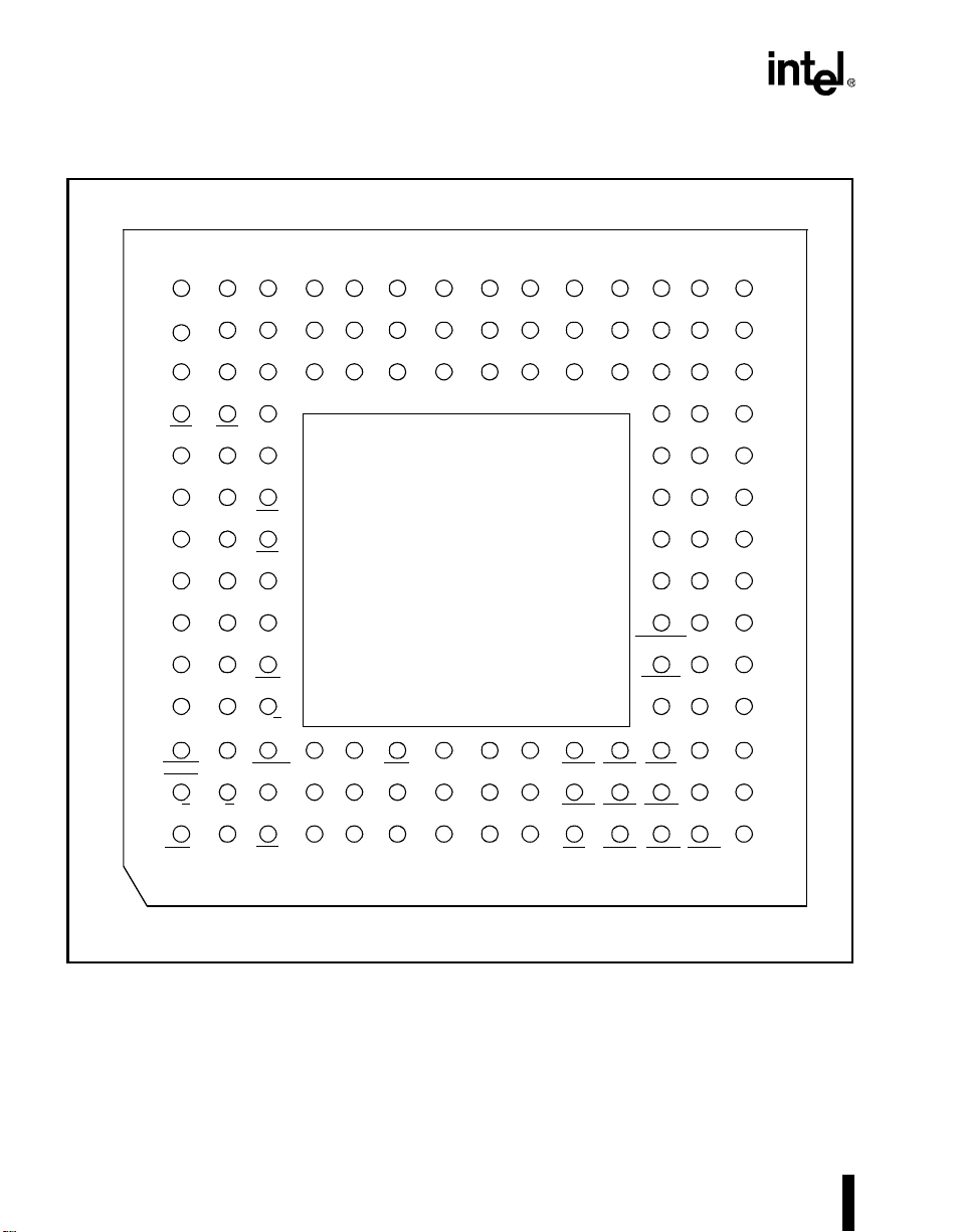
3.1.2 80960Jx 132-Lead PGA Pinout
1413121110987654321
P
AD25
AD18AD19AD22
CC
CC
CC
CC
CC
CC
AD13V
CC
AD6AD11
V
V
V
V
V
V
N
V
AD20AD24AD26AD27
SS
SS
SS
SS
SS
SS
SS
AD3AD7AD10
V
V
V
V
V
V
M
AD29AD30 NC
AD21AD23
AD14AD15AD16AD17
L
BE3
BE2
K
V
CC
AD28
V
AD31
SS
J
V
CC
H
G
F
E
D
C
B
V
CC
CC
V
CC
V
CC
V
CC
LOCK/
ONCE
A
SS
V
SS
V
V
V
SS
HOLDA
WIDTH/ADS
HLTD1
SS
SS
SS
BE1V
BE0
ALEV
BSTAT
DEN
DT/RV
A2
A3 XINT1
BLAST
HLTD0
NCTDOWIDTH/D/CW/R XINT4
NCNCALE
CC5
V
V
SS
SS
V
V
CC
CC
V
SS
SS
V
CC
CC
AD9AD12
AD8
AD5
AD2
NC
V
CCPLL
NC
RDYRCV
RESET
TDI
XINT0
XINT6V
XINT5XINT7NMIV
AD4
AD1
V
V
V
V
V
V
TCKXINT3
AD0
V
CC
V
CC
SS
V
CC
SS
CLKINV
SS
V
CC
SS
V
CC
SS
V
CC
SS
V
CC
SS
NCSTESTTRSTHOLDNCFAIL V
NC
TMSXINT2
P
N
M
L
K
J
H
G
F
E
D
C
B
A
12
1413121110987654321
Figure 3. 132-Lead Pin Grid Array Bottom View - Pins Facing Up
PRODUCT PREVIEW

PNMLKJHGFEDCBA
80960JD
14
TMS NC NC
13
12
11
10
9
8
7
6
5
4
3
2
1
TCK STEST
XINT2
XINT5
XINT3 TRST
XINT4
XINT7
NMI XINT6
VCCVSSHOLD
V
CCVSS
V
CCVSS
VCCVSSFAIL
NC
NC A2
NC TDO
WIDTH/
ALE
HLTD0
WIDTH/
D/C
HLTD1
ADS
W/R
V
CCVCCVCCVCC
V
SSVSSVSSVSSVSSVSSVSS
TDI
RESET
RDYRCV NC V
XINT0
XINT1
A80960JD
NC
V
CC5
A3
BLAST
DT/R
HOLDA
VCCVCCVCCVCCVCCVCCVCCBE2 AD30
LOCK/
ONCE
i
XXXXXXXX C0
BSTAT ALE
DEN
V
V
SS
SSVSSVSSVSSVSSVSS
M
©19xx
CLKIN
CCPLL
BE0
V
CCVCCVCC
AD2 AD5
NC
BE1
AD31
AD0 AD3 AD6
AD1 AD4 AD7 AD11
AD10 AD13AD8
AD9
V
SSVCC
AD12 VSSV
AD14
V
SSVCC
AD15 VSSV
AD16
AD17
AD21 VSSV
AD23 AD20 AD18
AD28
NC
BE3 AD29
V
V
SS
V
V
SS
AD19
AD24
AD22
AD26
AD27 AD25
CC
CC
CC
CC
CC
14
13
12
11
10
9
8
7
6
5
4
3
2
1
PNMLKJHGFEDCBA
Figure 4. 132-Lead Pin Grid Array Top View - Pins Facing Down
PRODUCT PREVI EW 13

80960JD
Table 6. 132-Lead PGA Pinout — In Signal Order
Signal Pin Signal Pin Signal Pin Signal Pin
A2 C5 AD31 K3 TDO B4 V
A3 C4 ADS
AD0 M14 ALE G3 TRST
AD1 L13 ALE
AD2 K12 BE0
AD3 N14 BE1
AD4 M13 BE2
AD5 L12 BE3
AD6 P14 BLAST
AD7 N13 BSTAT F3 V
AD8 M12 CLKIN H14 V
AD9 M11 D/C
AD10 N12 DEN
AD11 P13 DT/R
AD12 M10 FAIL
AD13 P12 HOLD C9 V
AD14 M9 HOLDA C2 V
AD15 M8 LOCK
/ONCE C1 V
AD16 M7 NC A4 V
AD17 M6 NC A5 V
AD18 P4 NC B5 V
AD19 P3 NC B14 V
AD20 N4 NC C8 V
AD21 M5 NC C14 V
AD22 P2 NC G12 V
AD23 M4 NC J12 V
AD24 N3 NC M3 V
AD25 P1 NMI
AD26 N2 RDYRCV
AD27 N1 RESET
AD28 L3 STEST C13 V
AD29 M2 TCK B13 V
AD30 M1 TDI D12 V
A1 TMS A14 V
C12 V
A3 V
H3 V
J3 V
L1 V
L2 V
C3 V
B2 V
E3 V
D3 V
C6 V
A10 V
F12 V
E12 V
CC
CC
CC
CC
CC
CC
CC
CC
CC
CC
CC
CC
CC
CC
CC
CC
CC
CC
CC
CC
CC
CC
CC
CC
CC
CCPLL
CC5
SS
SS
SS
A6 V
A7 V
A8 V
A9 V
D1 V
D14 V
E1 V
E14 V
F1 V
F14 V
G1 V
G14 V
H1 V
J1 V
J14 V
K1 V
K14 V
L14 V
P5 V
P6 W/R B1
P7 WIDTH/HLTD0 B3
P8 WIDTH/HLTD1 A2
P9 XINT0 C11
P10 XINT1 C10
P11 XINT2 A13
H12 XINT3 B12
C7 XINT4 B11
B6 XINT5 A12
B7 XINT6 B10
B8 XINT7 A11
SS
SS
SS
SS
SS
SS
SS
SS
SS
SS
SS
SS
SS
SS
SS
SS
SS
SS
SS
SS
SS
SS
NOTE: Do not connect any ext ernal logic to pins mark ed NC (no connect pins).
B9
D2
D13
E2
E13
F2
F13
G2
G13
H2
H13
J2
J13
K2
K13
N5
N6
N7
N8
N9
N10
N11
14
PRODUCT PREVIEW

Table 7. 132-Lead PGA Pinout — In Pin Order
Pin Signal Pin Signal Pin Signal Pin Signal
A1 ADS
A2 WIDTH/HLTD1 C7 V
A3 ALE
C6 FAIL H1 V
CC5
H2 V
C8 NC H3 BE0 M12 AD8
A4 NC C9 HOLD H12 V
A5 NC C10 XINT1
A6 V
A7 V
A8 V
A9 V
CC
CC
CC
CC
A10 NMI
A11 XINT7 D2 V
C11 XINT0 H14 CLKIN N1 AD27
C12 TRST J1 V
C13 STEST J2 V
C14 NC J3 BE1 N4 AD20
D1 V
CC
SS
H13 V
J12 NC N5 V
J13 V
A12 XINT5 D3 DT/R J14 V
A13 XINT2 D12 TDI K1 V
A14 TMS D13 V
B1 W/R D14 V
B2 D/C E1 V
B3 WIDTH/HLTD0 E2 V
SS
CC
CC
SS
B4 TDO E3 DEN
B5 NC E12 RESET
B6 V
B7 V
B8 V
B9 V
SS
SS
SS
SS
B10 XINT6
E13 V
E14 V
F1 V
F2 V
SS
CC
CC
SS
F3 BSTAT L14 V
K2 V
K3 AD31 N10 V
K12 AD2 N11 V
K13 V
K14 V
L1 BE2 N14 AD3
L2 BE3 P1 AD25
L3 AD28 P2 AD22
L12 AD5 P3 AD19
L13 AD1 P4 AD18
CC
SS
CCPLL
SS
CC
SS
SS
CC
CC
SS
SS
CC
CC
M10 AD12
M11 AD9
M13 AD4
M14 AD0
N2 AD26
N3 AD24
N6 V
N7 V
N8 V
N9 V
N12 AD10
N13 AD7
P5 V
B11 XINT4 F12 RDYRCV M1 AD30 P6 V
B12 XINT3 F13 V
B13 TCK F14 V
B14 NC G1 V
C1 LOCK/ONCE G2 V
SS
CC
CC
SS
M2 AD29 P7 V
M3 NC P8 V
M4 AD23 P9 V
M5 AD21 P10 V
C2 HOLDA G3 ALE M6 AD17 P11 V
C3 BLAST G12 NC M7 AD16 P12 AD13
C4 A3 G13 V
C5 A2 G14 V
SS
CC
M8 AD15 P13 AD11
M9 AD14 P14 AD6
NOTE: Do not connect any ext ernal logic to pins mark ed NC (no connect pins).
80960JD
SS
SS
SS
SS
SS
SS
SS
CC
CC
CC
CC
CC
CC
CC
PRODUCT PREVI EW 15

80960JD
3.1.3 80960Jx PQFP Pinout
V
RDYRCV
V
CC
SS
(I/O)
(I/O)
TDI
V
STEST
NC
(Core)
NC
V
SS
RESET
V
NC
V
CC
SS
V
CLKIN
(CLK)
(CLK)
CCPLL
CC
(Core)
NC
V
V
V
V
CC
CC
SS
SS
(Core)
(Core)
V
V
CC
SS
(Core)
(Core)
(I/O)
(I/O)
AD1
AD0
V
V
CC
SS
(I/O)
(I/O)
AD3
AD2
AD4
AD8
AD7
AD6
AD5
TRST
TCK
TMS
HOLD
XINT0
XINT1
XINT2
XINT3
VCC (I/O)
V
(I/O)
SS
XINT4
XINT5
XINT6
XINT7
NMI
VCC (Core)
V
(Core)
SS
NC
NC
V
CC5
NC
NC
FAIL
ALE
TDO
V
(I/O)
CC
V
(I/O)
SS
WIDTH/HLTD1
V
(Core)
CC
V
(Core)
SS
WIDTH/HLTD0
A2
A3
132
129
130
131
125
126
127
128
121
122
123
124
117
118
119
120
113
114
115
116
109
110
111
112
105
106
107
108
1
2
3
4
5
6
7
8
9
10
11
12
13
14
15
16
17
18
19
i960
®
20
21
22
23
24
25
26
27
28
29
30
31
32
33
35
34
39
38
37
36
43
42
41
40
NG80960JX
XXXXXXXX C0
M
46
48
47
© 19xx
49
i
45
44
62
61
60
59
58
57
56
55
54
53
52
51
50
100
101
102
103
104
AD9
99
98
V
(I/O)
CC
(I/O)
V
97
96
95
94
93
92
91
90
89
88
87
86
85
84
83
82
81
80
79
78
77
76
75
74
73
72
71
70
69
68
67
66
65
64
63
SS
AD10
AD11
V
CC
V
SS
V
CC
V
SS
AD12
AD13
AD14
AD15
V
CC
V
SS
AD16
AD17
AD18
AD19
V
CC
V
SS
AD20
AD21
AD22
AD23
V
CC
V
SS
V
CC
V
SS
AD24
AD25
AD26
NC
(I/O)
(I/O)
(Core)
(Core)
(I/O)
(I/O)
(I/O)
(I/O)
(Core)
(Core)
(I/O)
(I/O)
16
BLAST
V
W/R
ADS
D/C
V
CC
SS
(Core)
(Core)
DEN
DT/R
V
V
CC
SS
(I/O)
(I/O)
V
CC
SS
(Core)
(Core)
BSTAT
LOCK
V
V
CC
SS
(I/O)
(I/O)
/ONCE
V
ALE
HOLDA
BE0
BE1
BE2
BE3
AD27
V
V
V
CC
SS
CC
SS
(Core)
(I/O)
(Core)
(I/O)
V
CC
SS
(I/O)
(I/O)
AD28
AD29
AD30
AD31
V
V
Figure 5. 132-Lead PQFP - Top View
PRODUCT PREVIEW

Table 8. 132-Lead PQFP Pinout — In Signal Order
Signal Pin Signal Pin Signal Pin Signal Pin
AD31 60 ALE
AD30 61 ADS
24 VCC (Core) 47 V
36 VCC (Core) 59 VSS (I/O) 10
AD29 62 A3 33 V
AD28 63 A2 32 V
AD27 66 BE3
AD26 68 BE2
AD25 69 BE1
AD24 70 BE0
55 VCC (Core) 113 V
54 VCC (Core) 115 V
53 V
52 VCC (I/O) 9 V
AD23 75 WIDTH/HLTD1 28 V
AD22 76 WIDTH/HLTD0 31 V
AD21 77 D/C
AD20 78 W/R
AD19 81 DT/R
AD18 82 DEN
AD17 83 BLAST
AD16 84 RDYRCV
AD15 87 LOCK
/ONCE 50 V
35 V
37 V
42 V
43 V
34 V
132 V
AD14 88 HOLD 4 V
AD13 89 HOLDA 44 V
AD12 90 BSTAT 51 V
AD11 95 CLKIN 117 V
AD10 96 RESET
125 V
AD9 99 STEST 128 V
AD8 100 FAIL
23 VSS (CLK) 118 NC 127
AD7 101 TCK 2 V
AD6 102 TDI 130 V
AD5 103 TDO 25 V
AD4 104 TRST
1VSS (Core) 46 XINT4 11
AD3 107 TMS 3 V
AD2 108 V
AD1 109 V
AD0 110 V
ALE 45 V
(CLK) 120 VSS (Core) 73 XINT2 7
CC
(Core) 16 VSS (Core) 91 XINT1 6
CC
(Core) 29 VSS (Core) 114 XINT0 5
CC
(Core) 39 VSS (Core) 116 NMI 15
CC
(Core) 74 VSS (I/O) 27
CC
(Core) 92 V
CC
(Core) 123 V
CC
(I/O) 26 V
CC
(I/O) 41 V
CC
(I/O) 49 V
CC
(I/O) 57 V
CC
(I/O) 65 V
CC
(I/O) 72 V
CC
(I/O) 80 V
CC
(I/O) 86 NC 18
CC
(I/O) 94 NC 19
CC
(I/O) 98 NC 21
CC
(I/O) 105 NC 22
CC
(I/O) 111 NC 67
CC
(I/O) 129 NC 121
CC
CCPLL
CC5
(Core) 17 XINT7 14
SS
(Core) 30 XINT6 13
SS
(Core) 38 XINT5 12
SS
(Core) 58 XINT3 8
SS
119 NC 122
20 NC 126
(Core) 124
SS
(I/O) 40
SS
(I/O) 48
SS
(I/O) 56
SS
(I/O) 64
SS
(I/O) 71
SS
(I/O) 79
SS
(I/O) 85
SS
(I/O) 93
SS
(I/O) 97
SS
(I/O) 106
SS
(I/O) 112
SS
(I/O) 131
SS
NOTE: Do not connect any ext ernal logic to pins mark ed NC (no connect pins).
80960JD
PRODUCT PREVI EW 17

80960JD
Table 9. 132-Lead PQFP Pinout — In Pin Order
Pin Signal Pin Signal Pin Signal Pin Signal
1TRST
2 TCK 35 D/C
3TMS36ADS
4HOLD37W/R
5XINT0
6XINT1
7XINT2
8XINT3
9V
10 V
(I/O) 42 DT/R 75 AD23 108 AD2
CC
(I/O) 43 DEN 76 AD22 109 AD1
SS
11 XINT4
12 XINT5
13 XINT6
14 XINT7
15 NMI
16 V
17 V
(Core) 49 V
CC
(Core) 50 LOCK/ ONCE 83 AD17 116 V
SS
34 BLAST 67 NC 100 AD8
68 AD26 101 AD7
69 AD25 102 AD6
70 AD24 103 AD5
38 VSS (Core) 71 V
39 V
40 V
41 V
(Core) 72 V
CC
(I/O) 73 V
SS
(I/O) 74 V
CC
(I/O) 104 AD4
SS
(I/O) 105 V
CC
(Core) 106 V
SS
(Core) 107 AD3
CC
44 HOLDA 77 AD21 110 AD0
45 ALE 78 AD20 111 V
46 V
47 V
48 V
(Core) 79 V
SS
(Core) 80 V
CC
(I/O) 81 AD19 114 V
SS
(I/O) 82 AD18 115 V
CC
(I/O) 112 V
SS
(I/O) 113 V
CC
18 NC 51 BSTAT 84 AD16 117 CLKIN
19 NC 52 BE0
20 V
CC5
53 BE1 86 V
85 V
(I/O) 118 V
SS
(I/O) 119 V
CC
21 NC 54 BE2 87 AD15 120 V
22 NC 55 BE3 88 AD14 121 NC
23 FAIL
24 ALE
25 TDO 58 V
26 V
27 V
(I/O) 59 V
CC
(I/O)60AD3193V
SS
28 WIDTH/HLTD1 61 AD30 94 V
29 V
30 V
(Core) 62 AD29 95 AD11 128 STEST
CC
(Core) 63 AD28 96 AD10 129 V
SS
31 WIDTH/HLTD0 64 V
32 A2 65 V
56 V
57 V
(I/O) 89 AD13 122 NC
SS
(I/O) 90 AD12 123 V
CC
(Core) 91 V
SS
(Core) 92 V
CC
(I/O) 97 V
SS
(I/O) 98 V
CC
(Core) 124 VSS (Core)
SS
(Core) 125 RESET
CC
(I/O) 126 NC
SS
(I/O) 127 NC
CC
(I/O) 130 TDI
SS
(I/O) 131 V
CC
33 A3 66 AD27 99 AD9 132 RDYRCV
NOTE: Do not connect any ext ernal logic to pins mark ed NC (no connect pins).
(I/O)
CC
(I/O)
SS
(I/O)
CC
(I/O)
SS
(Core)
CC
(Core)
SS
(Core)
CC
(Core)
SS
(CLK)
SS
CCPLL
CC (CLK)
(Core)
CC
(I/O)
CC
(I/O)
SS
18
PRODUCT PREVIEW

80960JD
3.2 Package Thermal Specifications
The 80960JD is specified for operation when T
(case temperature) is within the range of 0°C to
100°C for both PGA and PQFP packages. Case
temperature may be measured in any environment
to determine whether the 80960JD is within its
specified operating range. The case temperature
should be measured at the center of the top surface,
opposite the pins.
θ
is the thermal resistance from case to ambient.
CA
Use the following equation to calculate T
maximum ambient temperature to conform to a
particular case temperature:
T
= TC - P (θCA)
A
Junction temperature (T
reliability calculations. T
(thermal resistance from junction to case) using the
) is commonly used in
J
can be calculated from θ
J
following eq uation:
T
= TC + P (θJC)
J
Table 10. 132-Lead PGA Package Thermal Characteristics
Thermal Resistance — °C/Watt
Parameter
θ
(Junctio n- t o-Case)
JC
θ
(Case-to-Ambient) (No Heatsink)
CA
θ
(Case-to-Ambient) (Omnidirectional Heatsink) 1596544
CA
θ
(Case-to-Ambient) (Unidirectional Heatsink) 1686544
CA
, the
A
Similarly, if T
temperature (T
C
= TA + P (θCA)
T
C
Compute P by multiplying I
V
. Values for θJC and θCA are given in Table 10
CC
for the PGA package and Table 11 for the PQFP
is known, the corresponding case
A
) can be calculate d as follows:
C
from Table 14 and
CC
package. For high speed operation, the processor’s
θ
may be significantly reduced by adding a
JA
heatsink and/or by increasing airflow.
Table 12 shows the maximum ambient temperature
(T
) permitted without exceeding TC for both PGA
A
and PQFP packages. The values are based on
typical I
+100°C.
JC
and VCC of +3.3 V, with a T
CC
Airflow — ft./min (m/sec)
0
200
400
600
800
(0)
(1.01)
(2.03)
(3.04)
(4.06)
0.7 0.7 0.7 0.7 0.7 0.7
25 19 14 12 11 10
1000
(5.08)
CASE
of
NOTES:
θ
J-PIN
θ
JA
θ
CA
θ
JC
θ
J-CAP
1. This table appli e s to a PGA device plugged into a socket or soldered direct ly into a board.
= θJC + θ
2. θ
3. θ
4. θ
5. θ
6. θ
7. θ
8. θ
JA
J-CAP
J-PIN
J-PIN
J-CAP
J-PIN
J-PIN
CA
= 5.6°C/W (approx.) (no heatsink)
= 6.4°C/W (inner pins) (approx.) (no heatsink)
= 6.2°C/W (outer pins) (approx.) (no heatsink )
= 3°C/W (approx.) (wi th heatsink)
= 3.3°C/W (inner pins) (approx.) (with heatsink)
= 3.3°C/W (outer pins) (approx.) (with heatsink)
PRODUCT PREVI EW 19

80960JD
Table 11. 132-Lead PQFP Package Thermal Characteristics
Thermal Resistance — °C/Watt
Airflow — ft./min (m/sec)
Parameter
θ
(Junctio n- t o-Case)
JC
θ
(Case-to-Ambie nt - N o Heatsin k)
CA
NOTES:
0
(0)50(0.25)
100
(0.50)
4.1 4.3 4.3 4.3 4.3 4.7 4.9 5.3
23 19 18 16 14 11 9 8
θ
JA
θ
JB
θ
θ
JC
θ
JL
1. This table applies to a PQFP device soldered directly int o board.
2. θ
= θJC + θ
JA
3. θJL = 13°C/W (approx.)
4. θ
= 13.5°C/W (approx.)
JB
CA
CA
200
(1.01)
400
(2.03)
600
(3.04)
800
(4.06)
1000
(5.08)
20
PRODUCT PREVIEW

80960JD
Table 12. Maximum T
at Various Airflows in °C
A
Airflow-ft/min (m/sec)
0
PQFP
Package
PGA
Package
f
(MHz)
CLKIN
T
without Heatsink 66
A
50
40
T
without Heatsink 66
A
50
40
TA with Omni Heatsink
1
66
50
40
TA with Uni-directional
Heatsink
2
66
50
40
1. 0.248” high omnidirectional heatsink (AI alloy 6061, 41mil fin width, 124 mil center-to-center fin spacing)
2. 0.250” high unidirectional heatsink (AI alloy 6061, 50 mil fin width, 146 mil center-to-center fin spacing)
(0)
61
70
77
58
68
75
75
81
85
73
79
84
200
(1.01)
73
79
84
68
75
81
85
88
91
86
90
92
400
(2.03)
76
82
86
76
82
86
90
92
94
90
92
94
600
(3.04)
81
86
89
80
84
88
92
94
95
92
94
95
800
(4.06)
85
88
91
81
86
89
93
95
96
93
95
96
1000
(5.07)
86
90
92
83
87
90
93
95
96
93
95
96
3.3 Thermal Management Accessories
The following is a list of suggested sources for 80960JD th ermal solutions. This is neither an endorsement or a
warranty of the performance of any of the listed products and/or companies.
Heatsinks
1. Thermallo y, Inc.
2021 West Valley Vi ew Lane
Dallas, TX 75234-8993
(214) 243-4321 FAX: (214) 241-4656
2. Wakefield Engi neering
60 Audubon Road
Wakefield, MA 01880
(617) 245-5900
3. Aavid Thermal Tech nologies, Inc.
One Kool Path
Laconia, NH 03247-0400
(603) 528-3400
PRODUCT PREVI EW 21

80960JD
4.0 ELECTRICAL SPECIFICATIONS
NOTICE: This document contains information on
products in the design phase of development. Do
4.1 Absolute Maximum Ratings
not finalize a design with this information. Revised
information will be published when the product
Parameter Maximum Rating
Storag e Temperat ure –65
Case Temperature Under Bias –65
Supply Voltage wrt.
Voltage on
Voltage on Other Pins wrt.
V
CC5
V
wrt. V
SS
SS
–0.5 V to + 4.6 V
–0.5 V to + 6.5 V
V
–0.5 V to VCC + 0.5 V
SS
o
C to +150oC
o
C to +110oC
becomes available.
sales office that you have the latest datasheet
before finaliz ing a design.
WARNING: Stressing the device beyond the
“Absolute Maximum Ratings” may cause permanent damage. These are stre ss ratings only. Operation beyond the “Operating Conditions” is not
recommended and extended exposure beyond the
“Operating Conditions” may affect device reli-
Verify with your local Intel
ability.
4.2 Operating Conditions
Table 13. 809 60JD Op erating Condi t ions
Symbol Parameter Min Max Units Notes
V
CC
V
CC5
f
CLKIN
T
C
NOTES:
1. See Section 4.4, V
Supply Voltage 3.15 3.45 V
Input Protection Bias 3.15 5.5 V (1)
Input Clock Frequency
80960JD-66
80960JD-50
80960JD-40
Operating Cas e Temperature (PGA
12
12
12
33.3
25
20
0100°C
MHz
and PQFP)
Pin Requirements (V
CC5
DIFF
) (pg. 23)
4.3 Connection Recommendations
For clean on-chip power distribution, VCC and V
pins separately feed the device’s functional units.
Power and ground connections must be made to all
80960JD power and ground pins. On the circuit
board, every V
plane and every V
plane. Place liberal decoupling capacitance near the
pin should connect to a power
CC
pin should connect to a ground
SS
80960JD, since the processor can cause transient
power surges.
22
SS
Pay special attention to the Test Reset (TRST
) pin. It
is essential that the JTAG Boundary Scan Test
Access Port (TAP) controller initializes to a known
state whether it will be used or not. If the JTAG
Boundary Scan function will be used, connect a
pulldown resistor between the TRST
pin and VSS. If
the JTAG Boundary Scan function will not be used
(even for board-level testing), connect the TRST
to V
. Also, do not con nect the TDI, TDO, and TCK
SS
pins if the TAP Controller will not be used.
pin
Pins identified as NC must not be connected in
the syst em.
PRODUCT PREVIEW

80960JD
4.4 V
Pin Requirements (V
CC5
DIFF
)
As shown in Figure 6, place a 100Ω resistor in series
with the V
pin to limit the current through V
CC5
In mixed voltage systems where the processor is
powered by 3.3 volts and interfaces with 5 volt
components, V
This allows proper 5 volt tolerant buffer operation,
must be connected to 5 volts.
CC5
+5 V (±0.25 V)
and prevents damage to the input pins. The voltage
differential between the 80960Jx V
volt V
requirement is not met, current flow through the pin
pins must not exceed 2.25 volts. If this
CC
pin and its 3.3
CC5
(±5%, 0.5 W)
may exceed the value at which the processor is
damaged. Instances when the voltage can exceed
2.25 volts is during power up or power down, where
one source reaches its level faster than the other,
briefly causing an excess voltage differential.
Another instance is during steady-state operation,
where the differential voltage of the regulator
(provided a regulator is used) cannot be maintained
within 2.25 volts. Two methods are possible to
prevent this from happening:
• Use a regulator that i s designed to preve nt the
voltage differential from exceeding 2.25 volts, or,
Figure 6. V
Current-Limiting Resistor
CC5
• If the regulator cannot prevent the 2.25 volt differential, the addition of the resistor is a simple and
reliable method for limiting current. The resistor
can also prevent damage in the case of a power
failure, wher e the 5 v olt s upp ly remai ns on and the
3.3 volt supply goes to zero.
In 3.3 volt only systems where the 80960Jx input
pins are driven from 3.3 volt logic, connect the V
pin directly to the 3.3 volt VCC plane.
Symbol Parameter Min Max Units Notes
V
DIFF
V
Difference
CC5-VCC
2.25 V V
input should not exceed VCC by more than 2.25 V
CC5
during power-up a nd power-d own, or d uring ste ady-state
operation.
4.5 V
Pin Requirements
CCPLL
To reduce clock jitter on the i960 Jx processor, the
V
pin for the Phase Lock Loop (PLL) circuit is
CCPLL
isolated on the pinout. The lowpass filter, as shown
tantalum), the 0.01 µF capacitor must be of the type
X7R and the node connecting V
short as possibl e.
in Figure 7, reduc es noise induced clock j i tter and its
effects on timing relationships in system designs.
The 4.7 µF capacitor must be (low ESR solid
100
.
CC5
V
Pin
CC5
Ω
CC5
must be as
CCPLL
100
Ω (±5%, 1/8 W)
V
CC
(Board Plan e)
Figure 7. V
+
4.7µF
CCPLL
0.01µF
Lowpass Filter
V
(On i960 Jx processors)
CCPLL
F_CA078A
PRODUCT PREVIEW 23

80960JD
4.6 DC Specifications
Table 14. 80960JD D C Characteristics
Symbol Parameter Min Typ Max Units Notes
V
IL
V
IH
V
OL
V
OH
V
OLP
C
IN
C
OUT
C
CLK
NOTES:
1. Typical is measured with VCC = 3.3 V and temperature = 25 °C.
2. Not tested.
Input Low Voltage -0.3 0.8 V
Input High Voltage 2.0 V
Output Low Voltage 0.4
Output High Voltage 2.4
V
- 0.2
CC
+ 0.3 V
CC5
0.2
VVIOL = 3 mA
I
OL
VI
OH
I
OH
Output Ground Bounce TBD V (1,2)
pF
pF
f
CLKIN
f
CLKIN
Input Capacitance
PGA
PQFP
I/O or Output Capacitance
PGA
PQFP
15
15
15
15
CLKIN Capacitance
PGA
PQFP
15
15
pF f
CLKIN
= 100 µA
= -1 mA
= -200 µA
= f
= f
= f
MIN
MIN
MIN
(2)
(2)
(2)
24
PRODUCT PREVIEW

Table 15. 809 60JD ICC Characteristics
Symbol Parameter Typ Max Units Notes
I
LI1
Input Leakage Current for
± 1
µA0 ≤ V
each pin exce pt TCK, TDI,
TRST and TMS
I
LI2
I
LO
R
pu
Input Leakage Current for
TCK, TDI,
TRST and TMS
Output Leakage Current ± 1 µA0.4 ≤ V
Internal Pull-UP
Resistance for
ONCE,
-140 -250
20 30 kΩ
µAV
TMS, TDI and TRST
I
Active
CC
(Power Supply)
Active
I
CC
(Thermal)
Test
I
CC
(Power modes)
80960JD-66
80960JD-50
80960JD-40
80960JD-66
80960JD-50
80960JD-40
Reset mode
80960JD-66
80960JD-50
80960JD-40
720
540
435
790
600
500
703
535
430
mA (2,3)
mA (2,4)
mA
Halt mode
Current on the
I
CC 5
V
Pin
CC5
80960JD-66
80960JD-50
80960JD-40
ONCE mode
80960JD-66
80960JD-50
80960JD-40
61
49
41
10
200
200
200
µA (6)
IN
= 0.45V (1)
IN
(2,3)
(2,3)
(2,4)
(2,4)
(5)
(5)
(5)
(5)
(5)
(5)
(5)
≤ V
OUT
80960JD
CC
≤ V
CC
PRODUCT PREVI EW 25

80960JD
4.7 AC Specifications
The 80960JD AC timings are based upon device characterization.
Table 16. 80960JD A C Characteristics (Sheet 1 of 2)
Symbol Parameter Min Max Units Notes
INPUT CLOCK TIMINGS
T
T
T
T
T
T
T
T
T
F
c
CS
CH
CL
CR
CF
OV1
OV2
CLKIN Frequency
80960JD-66
80960JD-50
80960JD-40
12
12
12
33.3
25
20
MHz
CLKIN Period
80960JD-66
80960JD-50
80960JD-40
30
40
12
83.3
83.3
83.3
ns
CLKIN Period Stability ± 250 ps (1, 2)
CLKIN High Time 8 ns Measured at 1.5 V (1)
CLKIN Low Time 8 ns Measured at 1.5 V (1)
CLKIN Rise Time 4 ns 0.8 V to 2.0 V (1)
CLKIN Fall Time 4 ns 2.0 V to 0.8 V (1)
SYNCHRONOUS OUTPUT TIMINGS
Output Va li d Dela y, E xce pt ALE/ ALE
Inactive and DT/R
for 3.3V input sig-
2.5
13.5
ns
(3)
nals.
Same as above, but for 5.5V input
signals.
2.5
16.5
Output Valid Delay, DT/R 0.5TC + 7 0.5TC + 9ns
T
OF
Output Float Delay 2.5 13.5 ns (4)
SYNCHRONOUS INPUT TIMINGS
T
IS1
T
IH1
T
IS2
T
IH2
T
IS3
T
IH3
T
IS4
T
IH4
NOTES: See Table 17 on page 28 for note definitions for this table.
Input Setup to CLKIN — AD31:0,
NMI, XINT7:0
Input Hold from CLKIN — AD31:0,
NMI, XINT7:0
Input Setup to CLKIN — RDYRCV
and HOLD
Input Hold from CLKIN — RDYRCV
and HOLD
Input Setup to CLKIN — RESET 7ns(7)
Input Hold from CLKIN — RESET 2ns(7)
Input Setup to RESET — ONCE,
STEST
Input Hold from RESET — ONCE,
STEST
26
6ns(5)
1.5 ns (5)
6.5 ns (6)
1ns(6)
7ns(8)
2ns(8)
PRODUCT PREVIEW

Table 16. 80960JD A C Characteristics (Sheet 2 of 2)
Symbol Parameter Min Max Units Notes
RELATIVE OUTPUT TIMINGS
T
T
T
T
LX
LXL
LXA
DXD
Address Valid to ALE/ALE Inactive 0.5TC - 5
ALE/ALE Width
(9)
Address Hold from ALE/ALE Inactiv e Equal Loading (9)
- 7 ns
0.5T
DT/R Valid to DEN Active Equal Loading (9)
C
BOUNDARY SCAN TEST SIGNAL TIMINGS
T
BSF
T
BSCH
T
BSCL
T
BSCR
T
BSCF
T
BSIS1
T
BSIH1
T
BSOV1
T
BSOF1
T
BSOV2
T
BSOF2
T
BSIS2
T
BSIH2
NOTES: See Table 17 on page 28 for note definitions for this table.
TCK Frequency 0.5TF MHz
TCK High Time 15 ns Measured at 1.5 V (1)
TCK Low Time 15 ns Measured at 1.5 V (1)
TCK Rise Time 5 ns 0.8 V to 2.0 V (1)
TCK Fall Time 5 ns 2.0 V to 0.8 V (1)
Input Setup to TCK — TDI, TMS 4 ns
Input Hold from T CK — TDI, TMS 6 ns
TDO Valid Delay 3 30 ns (1,10)
TDO Float Delay 3 30 ns (1,10)
All Outputs (No n-Test) Valid Delay 3 30 ns (1,10)
All Outputs (No n-Test) Float Delay 3 30 ns (1,10)
Input Setup to TCK — All Inputs
4ns
(Non-Test)
Input Hold fr om TCK — All Inputs
6ns
(Non-Test)
80960JD
PRODUCT PREVI EW 27

80960JD
Table 17. Note Definitions for Table 16, 80960JD AC Character istics (pg. 26)
NOTES:
1. Not tested .
2. To ensure a 1:1 relationship between the amplitude of the input jitter and the internal clock, the jitter
frequency spectrum should not have any power peaking between 500 KHz and 1/3 of the CLKIN
frequency.
3. Inactive ALE/ALE
timings, refer to Relative Output Timings in this table.
4. A float condition occurs when the output current becomes less than I
designed to be no longer than the v al id delay.
5. AD31:0 are synchronous inputs. Setup and hold times must be met for prop er processor operation. NMI
and XINT7:0 may be synchronous or asynchronous. Meeting setup and hold time guarantees recognition at a particular clock edge. For asynchronous operation, NMI
minimum of two CLKIN periods to guarantee recognition .
6. RDYRCV
operation.
7. RESET
8. ONCE
9. Guaranteed by design. May not be 100% tested.
10.Relative to falling edge of TCK.
11. W ors t- cas e T
may be synchronous or asynchronous. Meeting setup and ho ld time guarantees recognition at a
particular clock edge.
and STEST must be stabl e at the rising edge of RESET for proper operation.
low output state. The Address/Data Bus pins encounter this condition between the last ac cess of a read,
and the address cycle of a following write. 5 V signals take 3 ns longer to discharge than 3.3 V signals at
50 pF loads.
refers to the falling edge of ALE and the rising edge of ALE. For inactive ALE/ALE
. Float delay is not tested, but is
LO
and XINT7:0 must be asse rted fo r a
and HOLD are synchronous inputs. Setup and hold times must be met for proper processor
condition occurs on I/O pins when pins transition from a floating high input to driving a
OV
28
PRODUCT PREVIEW

4.7.1 AC Test Conditions and Derating Curves
80960JD
The AC Specifications in Section 4.7, AC Specification s are tested with the 50 pF load indicated in
Figure 8. Figure 9 shows how timings vary with load
capacitance; Figure 11 shows how output rise and
fall times vary with load capacit ance.
AC timings vs. load Cap
nom + 25
nom + 20
nom + 15
nom + 10
Tov (ns)
nom + 5
nom + 0
Output Valid Delay (ns) @ 1.5 V
50 100 150 200 250 300
Output Pin
CL (pF)
CL (pF)
C
L
Figure 8. AC Test Load
Capacitance
C
= 50 pF for all signals
L
Rising
Falling
Figure 9. Output Delay or Hold vs. Load Capacitance
PRODUCT PREVI EW 29
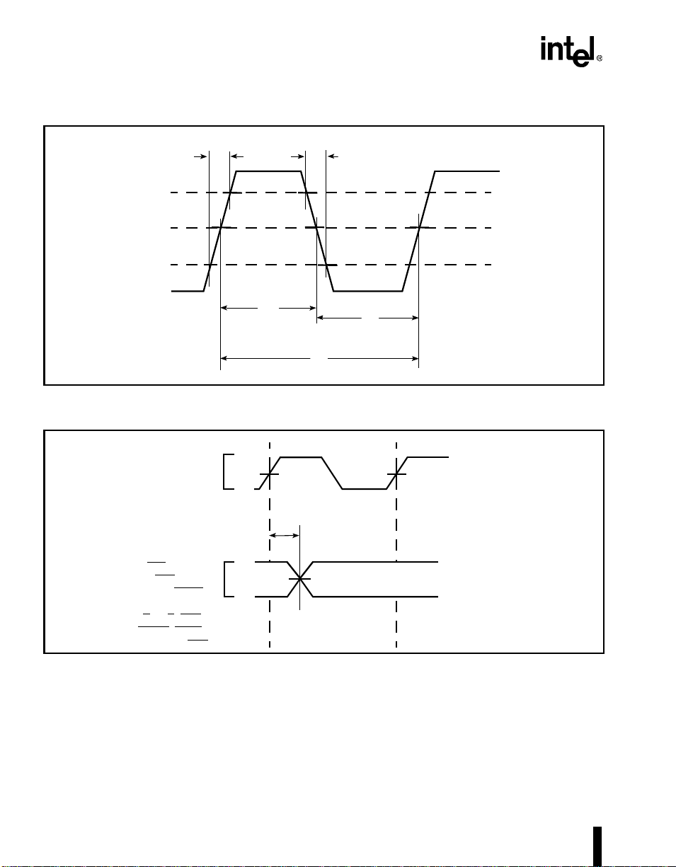
80960JD
4.7.2 AC Timing Wavefo rms
T
CLKIN
AD31:0,
ALE (active),
ALE (active),
ADS, A3:2 ,
BE3:0,
WIDTH/HLTD1:0,
D/
C, W/R, DEN,
BLAST, LOCK,
HOLDA, BSTAT,
CR
T
CH
T
CF
T
C
Figure 10. CLKIN Wavefo rm
1.5V
T
OV1
1.5V
FAIL
Figure 11. Output Delay Waveform for T
T
CL
1.5V
OV1
2.0V
1.5V
0.8V
30
PRODUCT PREVIEW

80960JD
CLKIN
AD31:0,
ALE
ALE,
ADS, A3:2,
WIDTH/HLTD1:0,
D/
DEN, BLAST, LOCK
BE3:0,
C, W/R, DT/R,
CLKIN
AD31:0
NMI
XINT7:0
1.5V
T
OF
1.5V
Figure 12. Output Float Waveform for TOF
T
IH1
Valid
1.5V
T
IS1
1.5V1.5V1.5V
Figure 13. Input Setup and Hold Waveform for T
IS1
and T
IH1
PRODUCT PREVI EW 31

80960JD
CLKIN
T
IS2
HOLD,
RDYRCV
1.5V
Valid
Figure 14. Input Setup and Hold Waveform for T
CLKIN
T
IH3
RESET
1.5V1.5V1.5V
T
IH2
1.5V
and T
IS2
1.5V1.5V
T
IS3
IH2
32
Figure 15. Input Setup and Hold Waveform for T
IS3
and T
IH3
PRODUCT PREVIEW

RESET
80960JD
T
T
IS4
IH4
ONCE,
STEST
Valid
Figure 16. Input Setup and Hold Waveform for T
T
a
CLKIN
T
LXL
ALE
ALE
AD31:0
1.5V
1.5V
Valid
T
LX
Valid
1.5V
T
LXA
Figure 17. Relative Timings Waveform for T
Tw/T
1.5V
LX
, T
d
IS4
LXL
and T
and T
IH4
LXA
1.5V1.5V1.5V
PRODUCT PREVI EW 33

80960JD
CLKIN
DT/R
DEN
T
a
1.5V
T
OV2
T
DXD
T
Figure 18. DT/R and DE N Timings Waveform
T
BSCR
T
BSCF
OV1
Tw/T
Valid
d
1.5V1.5V
2.0V
34
T
BSCH
T
BSCL
Figure 19. TCK Waveform
1.5V
0.8V
PRODUCT PREVIEW

80960JD
TCK
T
TMS
TDI
T
1.5V
BSIS1
BSIH1
Valid
Figure 20. Input Setup and Hold Waveforms for T
TCK
T
BSOV1
TDO
1.5V
Valid
1.5V
T
BSOF1
BSIS1
1.5V1.5V1.5V
and T
1.5V1.5V1.5V
BSIH1
Figure 21. Output Delay and Output Float Waveform for T
BSOV1
AND T
BSOF1
PRODUCT PREVI EW 35

80960JD
TCK
Non-Test
Outputs
1.5V
1.5V
T
BSOV2
1.5V
Valid
T
BSOF2
Figure 22. Output Delay and Output Float Waveform for T
TCK
T
Non-Test
Inputs
T
1.5V
BSIS2
Valid
BSIH2
1.5V
1.5V
BSOV2
1.5V1.5V1.5V
and T
BSOF2
36
Figure 23. Input Setup and Hold Waveform for T
BSIS2
and T
BSIH2
PRODUCT PREVIEW

80960JD
5.0 BUS FUNCTIONAL WAVEFORMS
Figures 24 through 29 illustrate typical 80960JD bus
transactions. Figure 30 depicts the bus arbitration
sequence. Figure 31 illustrates the processor reset
sequence from the time power is applied to the
device. Figure 32 illustrates the processor reset
sequence when the processor is in operation. Figure
TiTiTaTdTrTiT
CLKIN
AD31:0
ALE
ADS
A3:2
BE3:0
T
aTdTr
ADDR
D
In
33 illustrates the processor ONCE
sequence from
the time power is applied to the device. Figures 34
and 35 also show accesses on 32-bit buses. Tables
18 through 21 summarize all possible combinations
of bus accesses across 8-, 16-, and 32-bit buses
according to data alignment.
i
Invalid
ADDR
DATA Out
WIDTH1:0
D/
W/R
BLAST
DT/R
DEN
RDYRCV
C
10 10
F_JF030A
Figure 24. Non-Burst Read and Write Transaction s Without Wait States, 32-Bit Bus
PRODUCT PREVI EW 37

80960JD
CLKIN
AD31:0
ALE
ADS
A3:2
BE3:0
WIDTH1:0
D/
W/R
TaTdTdTrTaTdTdTdT
ADDR
D
D
In
In
ADDR
DATA
Out
DATA
Out Out
DATA
T
d
r
DATA
Out
00 or 10 01 or 11 00 01 10 11
1 0
1 0
C
38
BLAST
DT/R
DEN
RDYRCV
Figure 25. Burst Read and Write Transactions Without Wait States, 32-Bit Bus
PRODUCT PREVIEW
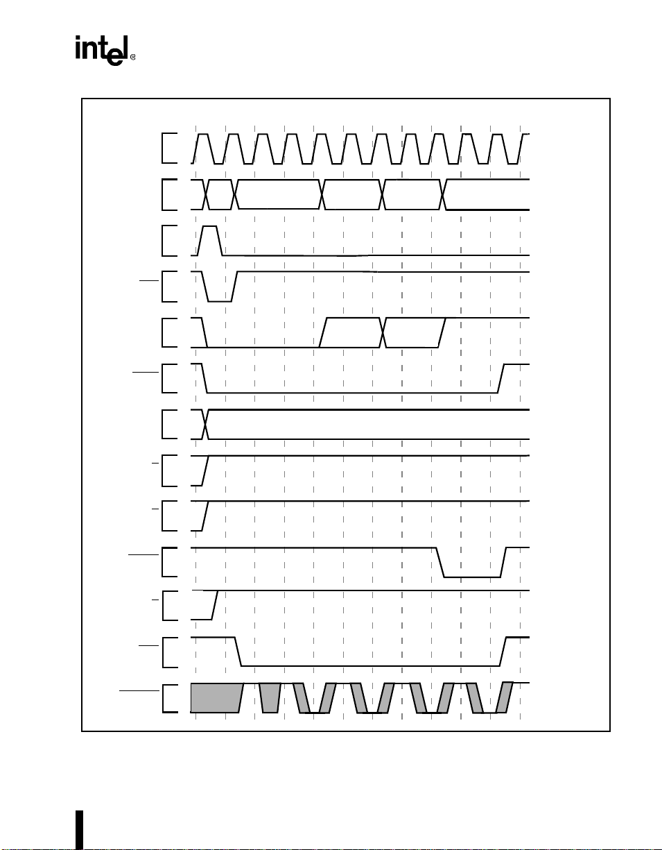
80960JD
CLKIN
AD31:0
ALE
ADS
A3:2
BE3:0
WIDTH1:0
D/
W/R
TaTwTwTdTwTdTwTdTwTdT
ADDR
0 0
DATA
Out
DATA
Out
0 1 1 0 1 1
DATA
Out
DATA
Out
r
1 0
C
BLAST
DT/R
DEN
RDYRCV
F_JF032A
Figure 26. Burst Write Transactions With 2,1,1,1 Wait States, 32-B it Bus
PRODUCT PREVI EW 39

80960JD
CLKIN
AD31:0
ALE
ADS
A3:2
BE1/A1
BE0/A0
WIDTH1:0
D/
W/R
TaTdTdTrTaTdTdTdT
ADDR
00 or 10
D
D
In
In
00,01, 10 or 11
01 or
11
00
DATA DATA
ADDR
Out
00,01,10 or 11
00 01 10 11
DATA
Out
Out
00
T
d
r
DATA
Out
C
40
BLAST
DT/R
DEN
RDYRCV
F_JF033A
Figure 27. Burst Read and Write Transactions Without Wait States, 8-Bit Bus
PRODUCT PREVIEW

CLKIN
AD31:0
ALE
ADS
TwTdTdTrTrTaTwTdTdT
T
a
D
ADDR
D
In
In
ADDR
DATA DATA
Out Out
80960JD
r
A3:2
BE1/A1
BE3/BHE
BE0/BLE
WIDTH1:0
D/
W/R
BLAST
DT/R
DEN
RDYRCV
00,01,10, or 11
0
01 01
1
00,01,10, or 11
01
C
F_JF034A
Figure 28. Burst Read and Write Tran sactions With 1, 0 Wait States
and Extra Tr State on Read, 16-Bit Bus
PRODUCT PREVI EW 41

80960JD
CLKIN
AD31:0
ALE
ADS
A3:2
BE3:0
WIDTH1:0
D/
W/R
TaT
AAA
1 1 0 1
C
TrTaT
d
D
In
00 00 01 10
A
0 0 1 1
TrTaT
d
D
In
0 0 0 0
1 0
Valid
TrTaT
d
D
In
d
1 1 1 0
T
r
D
In
42
BLAST
DT/R
DEN
RDYRCV
Figure 29. Bus Transactions Generated by Double Word Read Bus Request,
Misaligned One Byte From Quad Word Boundary, 32-Bit Bus, Little Endian
PRODUCT PREVIEW
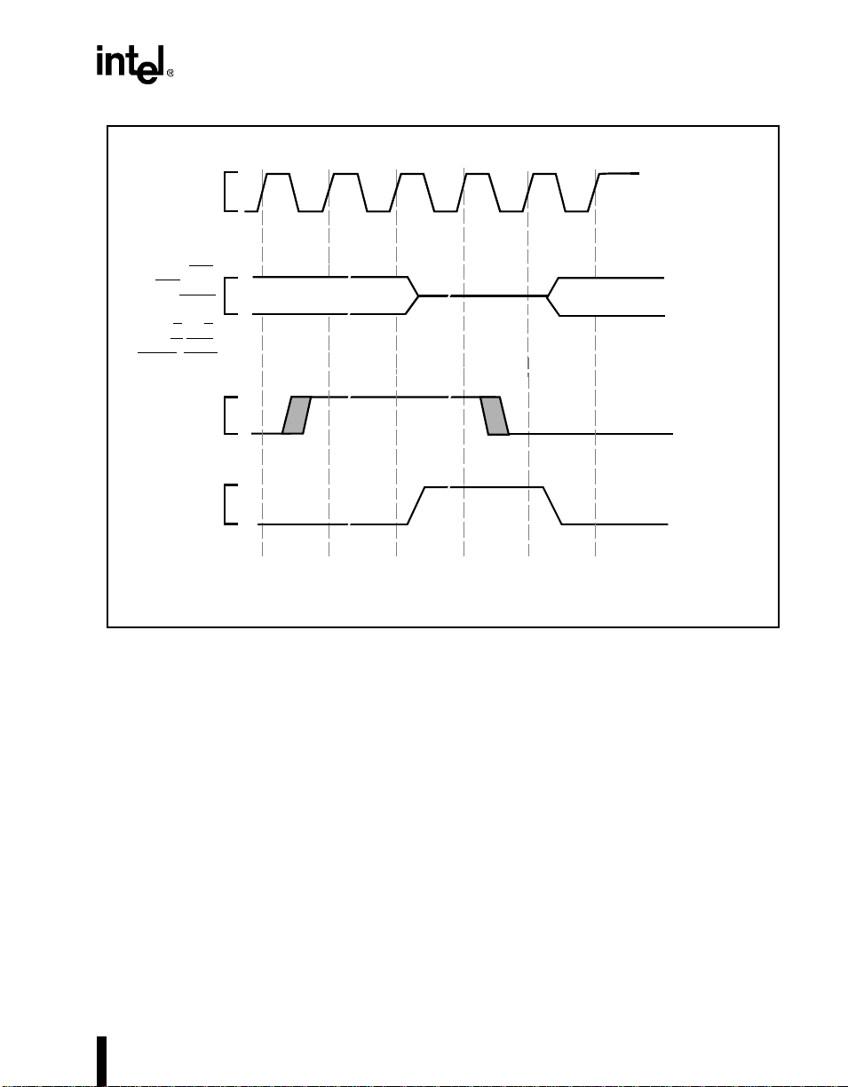
80960JD
Ti or T
∼
Valid
∼
∼
∼
∼
∼
∼
∼
(Note)
∼
∼
CLKIN
Outputs:
AD31:0,
ALE,
ALE,
ADS, A3:2 ,
WIDTH/HLTD1:0,
BE3:0,
D/
C, W/R,
R, DEN,
DT/
BLAST, LOCK
HOLD
HOLDA
NOTE: HOLD is sampled on the rising edge of CLKIN. The processor asserts HOLDA to grant the bus on the
same edge in which it recognizes HOLD if the last state was T
the proces sor deasse r ts H OLDA on th e same edge in which it recognizes th e deasserti on of HOLD .
Figure 30. HOLD/HOLDA Waveform For Bus Arbitration
T
r
h
T
h
∼
∼
∼
∼
∼
∼
∼
∼
or the last Tr of a bus tran saction. Similarly,
i
Ti or T
a
Valid
PRODUCT PREVI EW 43

80960JD
∼
∼
∼∼∼
First
Bus
Activity
(Note 1)
∼
∼
∼
∼
∼
∼
∼
∼
∼
∼
∼
∼
∼
∼
∼
∼
∼
∼
∼
∼
∼
Idle (Note 2)
Valid Input (Note 3)
∼
∼
∼
∼
∼
∼
∼
∼
∼
∼
∼
∼
∼
∼
Valid Output (Note 3)
∼
∼
∼
∼
∼
∼
∼
∼
∼∼∼
∼
(Output)
Built-in self-test, approx imately
207,000 CLKIN periods
(if selected)
(Input)
Valid
∼
∼
∼
∼∼∼
∼
∼
44
∼
∼
∼
∼
∼∼∼
∼
∼
∼
∼
CC
V
CLKIN
, ADS,
ALE
∼
∼
BE3:0, DEN,
∼
∼
BLAST
∼∼∼
DT/R
R,
ALE,W/
WIDTH/HLTD1:0
∼
∼
∼∼∼
∼
∼
∼∼∼
∼
∼
∼
∼
FAIL
AD31:0, A3:2,D/C
Figure 31. Cold Reset Waveform
∼∼∼
HOLD
∼
∼
∼
∼
∼
∼
ONCE
∼
∼
∼
STEST
RESET
∼
∼
and CLKIN stable to RESET High, minimum
CC
V
10,000 CLKIN periods, for PLL stabilization.
∼
∼
during the bus confidence test. If the bus confidence test passes, FAIL is deasserted and the processor begins user program execution.
Notes:
2. If the processor fails built-in self-test, it initiates one dummy load bus access. The load address indicates the point of self-test failure.
1. The processor asserts FAIL during built-in self-test. If self- test passes, the FAIL pin is deass er t e d .The process or also asserts FAI L
3. Since the bus is idle, hold requests are honored during reset and built-in self-test.
∼∼∼
∼
∼
∼
∼∼∼
∼
∼
∼
LOCK/
HOLDA
PRODUCT PREVIEW

80960JD
∼
∼
∼
∼
∼
∼
∼
∼
∼
∼
∼
∼
∼
∼∼∼
∼∼∼
∼
∼
∼∼∼
∼
∼
∼∼∼
∼
∼
∼
∼
∼
∼∼∼
∼
∼
∼∼∼
∼
∼
∼
∼
∼
∼
∼∼∼
∼
∼
∼
Valid
∼∼∼
∼
∼
∼
∼
4 CLKIN Cycles
Maximum RESET Low to Reset State
∼
∼
∼
RESET High to First Bus
Activity, 46 CLKIN Cycles
∼
∼
∼
∼
15 CLKIN Cycles
Minimum RESET Low Time
CLKIN
DEN, BLAST
ALE, ADS, BE3:0,
FAIL
WIDTH/HLTD1:0
ALE, W/R,DT/R, BSTAT,
Figure 32. Warm Reset Waveform
AD31:0, A3:2, D/C
HOLD
HOLDA
STEST
LOCK/ONCE
RESET
PRODUCT PREVI EW 45

80960JD
∼
∼
∼∼∼
∼
∼
∼
∼
∼
∼
∼∼∼
∼∼∼
∼
∼
∼
∼
(Input)
∼
∼
∼
∼
∼∼∼
∼
∼
∼
∼
∼
∼
∼∼∼
∼
∼∼∼
∼
∼
∼
∼
∼∼∼
∼
∼
∼∼∼
∼
∼
∼
∼
∼∼∼
∼
∼∼∼
∼
∼
∼
∼
(Note 1)
∼
∼
∼
∼
∼
and CLKIN stable to RESET High,
∼
∼
∼
∼
CC
V
minimum 10,000 CLKIN periods, for PLL
stabilization.
∼
∼
∼
∼
∼
∼
∼∼∼
∼
∼∼∼
∼
∼
∼∼∼
∼
∼
∼
∼
∼
∼∼∼∼∼
∼∼∼
CLKIN may not be allowed to float.
It must be driven hi gh or low or continue to run .
∼
∼
∼
∼
∼
∼
∼
∼
∼
∼
∼
∼
46
CLKIN
CC
V
,
D/C
FAIL
ALE,W/R
ALE, ADS,
BE3:0, DEN, BLAST
DT/R, WIDTH/HLTD1:0
Figure 33. Entering the ONCE State
HOLD
AD31:0, A3:2,
ONCE
LOCK/
STEST
HOLDA
RESET
NOTES:
1. ONCE mode may be entered prior to the rising edge of RESET: ONCE input is not latched until the rising edge of RESET.
2. The ONCE input may be removed after the processor enters ONCE Mode.
PRODUCT PREVIEW
Table 18. Natural Boundaries for Load and Store Accesses
Data Width Natural Boundary (Bytes)
Byte 1
Short Word 2
Word 4
Double Word 8
Triple Word 16
Quad Word 16
Table 19. Summary of Byte Load and Store Accesses
80960JD
Address Offset from
Natural Boundary
(in Bytes)
+0 (aligned)
Address Offset from
Natural Boundary
(in Bytes)
+0 (aligned)
+1 • 2 byte accesses • 2 byte accesses • 2 byte accesses
Accesses on 8-Bit Bu s
(WIDTH1:0=00)
• by te acces s • byte access • by te acces s
Table 20. Summary of Sh ort Word Load and Store Accesses
Accesses on 8-Bit Bu s
(WIDTH1:0=00)
• burst of 2 bytes • short-word access • short-word access
Accesses on 16 Bit
Bus (WIDTH1:0=01)
Accesses on 16 Bit
Bus (WIDTH1:0=01)
Accesses on 32 Bit
Bus (WIDTH1:0=10)
Accesses on 32 Bit
Bus (WIDTH1:0=10)
PRODUCT PREVI EW 47

80960JD
Address Offset
from Natural
Boundary in Bytes
+0 (aligned)
(
n
=1, 2, 3, 4)
+1 (n =1, 2, 3, 4)
n
= 2, 3, 4)
+5 (
+9 (
n
= 3, 4)
n
= 3, 4)
+13 (
+2 (n =1, 2, 3, 4)
n
= 2, 3, 4)
+6 (
+10 (
n
= 3, 4)
n
= 3, 4)
+14 (
+3 (n =1, 2, 3, 4)
+7 (
n
= 2, 3, 4)
n
= 3, 4)
+11 (
n
= 3, 4)
+15 (
+4 (n = 2, 3, 4)
+8 (
n
= 3, 4)
n
= 3, 4)
+12 (
Table 21. Summary of n-Word Load and Store Accesses (n = 1, 2, 3, 4)
Accesses on 8-Bit Bu s
(WIDTH1:0=00)
n
burst(s) of 4 bytes • case n=1:
•
• by te acces s
• burst of 2 bytes
•
n
-1 burst(s) of 4 by tes
• by te acces s
• burst of 2 bytes
•
n
-1 burst(s) of 4 by tes
• burst of 2 bytes
• by te acces s
•
n
-1 burst(s) of 4 by tes
• burst of 2 bytes
• by te acces s
n
burst(s) of 4 bytes •n burst(s) of 2 short words •n word access(es)
•
Accesses on 16 Bit Bu s
(WIDTH1:0=01)
burst of 2 short words
• case
n
=2:
burst of 4 short words
• case
n
=3:
burst of 4 short words
burst of 2 short words
• case
n
=4:
2 bursts of 4 short w ords
• by te acces s
• short-word access
•
n
-1 burst(s) of 2 short words
• by te acces s
• short-word access
•
n
-1 burst(s) of 2 short words
• short-word access
• byte access
•
n
-1 burst(s) of 2 short words
• short-word access
• by te acces s
Accesses on 32 Bit
Bus (WIDTH1:0=10)
• burst of
• byte access
• short-word access
•
n
-1 word access(es)
• byte access
• short-word access
•
n
-1 word access(es)
• short-word access
• byte access
•
n
-1 word access(es)
• short-word access
• byte access
n
word(s)
48
PRODUCT PREVIEW

80960JD
Byte Offset
Word Offset
Short-Word
Load/Store
Word
Load/Store
04 812162024
0123456
Short Access (Aligned)
Byte, Byte Accesses
Short Access (Aligned)
Byte, Byte Accesses
Word Acce ss (Aligned)
Byte, Short, Byte, A cces s es
Short, Short Accesses
Byte, Short, Byte Accesses
One Double-Word Burst (Ali gned)
Byte, Short, Word, Byte Accesses
Short, Word, Short Accesses
Double-Word
Load/Store
Byte, Word, Short, Byte Accesses
Word, Word Accesses
One Double-Word
Burst (Aligned)
Figure 34. Summary of Aligned and Unaligned Accesses (32- Bit Bus)
PRODUCT PREVI EW 49

80960JD
Byte Offset
Word Offset
Triple-Word
Load/Store
Quad-Word
Load/Store
04812162024
0123456
One Three-Word
Burst (Aligned)
Byte, Short, Word,
Word, Byte Accesses
Short, Word, Word,
Short Acce sses
Byte, Word, Word,
Short, Byte Accesses
Word, Word,
Word Accesses
Word, Wor d,
Word Acce sses
Word,
Word,
Word
Accesses
One Four-Word
Burst (Aligned)
Byte, Short, Word, Word,
Word, Byte Accesses
Short, Word, Word, Word,
Short Acce sses
Byte, Word, Word, Word,
Short, Byte Accesses
Word, Word, Word,
Word Accesses
Word,
Word,
Word,
Word,
Accesses
50
Figure 35. Summary of Aligned and Unalig n ed Accesses (32-Bit Bus) (Continued)
PRODUCT PREVIEW

80960JD
6.0 DEVICE IDENTIFICATION
80960JD processors may be identified electrically,
according to device type and stepping (see Figure
36, and Table 22 through Table 25). Table 22
identifies the device ID for all 3.3V and 5 V,
80960JD processors. Figure 36, and Table 23
through Table 25 identify all 3.3 V, 5 V-tolerant,
80960JD processors. The device ID for the C0
stepping is enhanced to differentiate between 3.3 V
and 5 V supply voltages, and between non-clock-
• Upon reset, the identi fier is placed into the g0
register.
• The identifier may be accessed from supervisor
mode at any time by reading the DEVICE ID
register at address FF008710H.
• The IEEE Standard 1149.1 Test Access Port may
select the DEV IC E ID register throu gh the
IDCODE instruction.
• The device and steppi ng l etter is also prin ted on
the top side of the product package.
doubled and clock-doubled cores when stepping
from the A2 stepping to the C0 stepping. The 32-bit
identifier is accessible in three ways:
Table 22. 80960JDDie and Stepping Referen ce
Device and
Stepping
Version
Number
Part Number Manufacturer X
Complete ID
80960JD A, A2 0000 1000 1000 0010 0000 0000 0001 001 1 08820013
80960JD C0 0011 0000 1000 0011 0000 0000 0001 001 1 30830013
Part Number
Product
V
Type
Version ModelGen
CC
Manufacturer ID
(Hex)
1
00001
40
110010000000
28 24 20
10000010000
16 12 8
Figure 36. 80960JD Device Identification Register
PRODUCT PREVI EW 51

80960JD
Table 23. Fiel ds of 80960JD Device ID
Field Va lue Definition
Version See Table 25 Indicates major stepping changes.
V
CC
Product Ty pe 00 0100
Generation Type 0001 = J-series In di cates the generat ion (or series) of prod uct.
Model D000C
Manufacturer ID 000 0000 1001
Device Version V
80960JD A, A2 See
80960JD C0 0 000100 0001 10000 00000001001 1
0 = 3.3 V dev ic e
1 = 5V device
(Indicates i960 CPU)
D = Clock Doubled
(0) Not Clock-Doubled
(1) Clock Doubled
C = Cache Size
(0) 4K I-cache, 2K D-cache
(1) 2K I-cache, 1K D-cache
(Indicates Intel)
Table 24. 80960JD Device ID Model Types
CC
1 000100 0001 00000 00000001001 1
Table 25
Product G en. Model Manufacturer ID ‘1’
Indicates that a device is 3.3V or 5.0 V.
Designates type of product.
Indicates member within a series and specific model
information.
Manufacturer ID assigned by IE EE.
Table 25. Device ID Version Numbers for Different Steppings
Stepping Version
A0 0000
A2 0000
C0 0011
NOTE: This data sheet applies to the 80960JD C0 stepping.
52
PRODUCT PREVIEW

7.0 REVISION HISTORY
This is the first revision of the 3.3 V device.
80960JD
PRODUCT PREVI EW 53
 Loading...