


*Other brands and names are the property of their respective owners.
Information in this document is provided in connection with Intel products. Intel assumes no liability whatsoever, including infringement of any patent or
copyright, for sale and use of Intel products except as provided in Intel’s Terms and Conditions of Sale for such products. Intel retains the right to make
changes to these specifications at any time, without notice. Microcomputer Products may have minor variations to this specification known as errata.
July 1994COPYRIGHT©INTEL CORPORATION, 1995 Order Number: 270909-006
8XC196KB/8XC196KB16
COMMERCIAL/EXPRESS CHMOS MICROCONTROLLER
Y
8 Kbytes of On-Chip ROM/OTP
Available
Y
232 Byte Register File
Y
Register-to-Register Architecture
Y
28 Interrupt Sources/16 Vectors
Y
1.75 ms 16 x 16 Multiply (16 MHz)
Y
3.0 ms 32/16 Divide (16 MHz)
Y
Powerdown and Idle Modes
Y
Five 8-Bit I/O Ports
Y
16-Bit Watchdog Timer
Y
12 MHz and 16 MHz Available
Y
Dedicated 15-Bit Baud Rate Generator
Y
Dynamically Configurable 8-Bit or
16-Bit Buswidth
Y
Full Duplex Serial Port
Y
High Speed I/O Subsystem
Y
16-Bit Timer
Y
16-Bit Up/Down Counter with Capture
Y
Pulse-Width-Modulated Output
Y
Four 16-Bit Software Timers
Y
10-Bit A/D Converter with Sample/Hold
Y
HOLD/HLDA Bus Protocol
Y
Extended Temperature Available
The 8XC196KB is a 16-bit microcontroller available in three different memory varieties: ROMless (80C196KB),
8K ROM (83C196KB) and 8K OTP (One Time ProgrammableÐ87C196KB). The 8XC196KB is a high performance member of the MCS
É
96 microcontroller family. The 8XC196KB has the same peripheral set as the
8096BH and has a true superset of the 8096BH instructions. Intel’s CHMOS process provides a high performance processor along with low power consumption. To further reduce power requirements, the processor can
be placed into Idle or Powerdown Mode.
Bit, byte, word and some 32-bit operations are available on the 80C196KB. With a 16 MHz oscillator a 16-bit
addition takes 0.50 ms, and the instruction times average 0.37 ms to 1.1 ms in typical applications.
Four high-speed capture inputs are provided to record times when events occur. Six high-speed outputs are
available for pulse or waveform generation. The high-speed output can also generate four software timers or
start an A/D conversion. Events can be based on the timer or up/down counter. Also provided on-chip are an
A/D converter, serial port, watchdog timer and a pulse-width-modulated output signal.
The 8XC196KB has a maximum guaranteed frequency of 12 MHz. The 8XC196KB16 has a maximum guaranteed frequency of 16 MHz. All references to the 80C196KB also refer to the 80C196KB16; 83C196KB, Rxxx;
87C196KB and 87C196KB16 unless otherwise noted. The ROM device does not have a speed indicator at the
end of the device name. Instead it has a ROM code number.
With the commercial (standard) temperature option, operational characteristics are guaranteed over the temperature range of 0
§
Ctoa70§C. With the extended temperature range option, operational characteristics are
guaranteed over the temperature range of
b
40§Ctoa85§C.
Package Designators: N
e
68-pin PLCC, Se80-pin QFP (commercial only). Prefix Designators: TeExtend-
ed Temperature.
*Other brands and names are the property of their respective owners.
8XC196KB/8XC196KB16
270909– 1
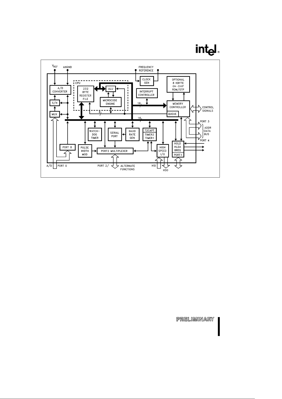
Figure 1. 8XC196KB Block Diagram
2
8XC196KB/8XC196KB16
PROCESS INFORMATION
This device is manufactured on P629.0 and 629.1, a
CHMOS III-E process. Additional process and reliability information is available in Intel’s
Components
Quality and Reliability Handbook,
Order Number
210997.
270909– 2
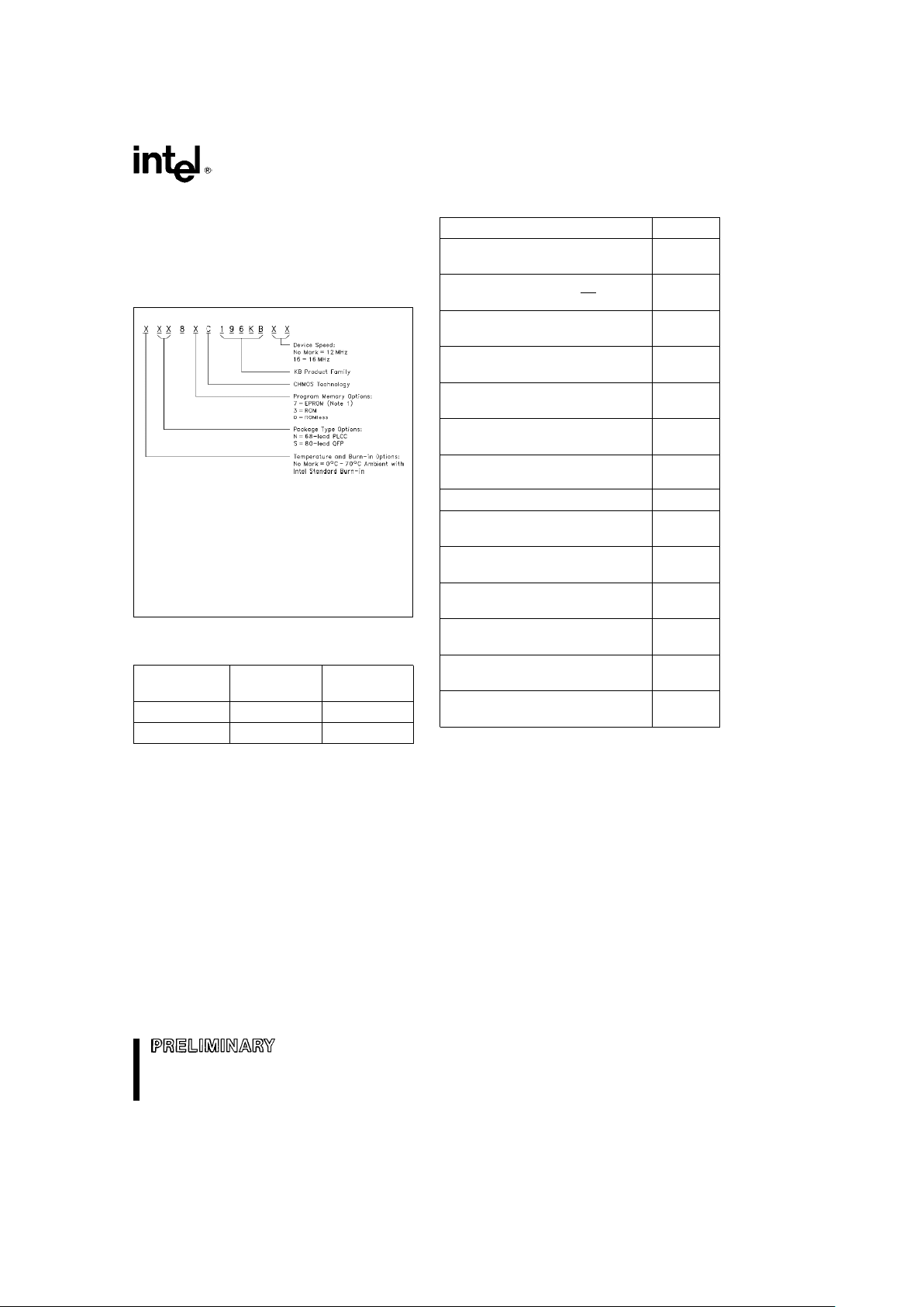
EXAMPLE: N87C196KB16 is 68-Lead PLCC
OTPROM, 16 MHz.
For complete package dimensional data, refer to the
Intel Packaging Handbook (Order Number 240800).
NOTE:
1. EPROMs are available as One Time Programmable
(OTPROM) only.
Figure 2. The 8XC196KB Nomenclature
Table 1. Thermal Characteristics
Package
i
ja
i
jc
Type
PLCC 35§C/W 13§C/W
QFP 70§C/W 4§C/W
All thermal impedance data is approximate for static air
conditions at 1W of power dissipation. Values will change
depending on operation conditions and application. See
the Intel
Packaging Handbook
(order number 240800) for a
description of Intel’s thermal impedance test methodology.
Table 2. 8XC196KB Memory Map
Description Address
External Memory or I/O 0FFFFH
04000H
Internal ROM/EPROM or External 3FFFH
Memory (Determined by EA
)
2080H
Reserved. Must contain FFH. 207FH
(Note 5)
2040H
Upper Interrupt Vectors 203FH
2030H
ROM/EPROM Security Key 202FH
2020H
Reserved. Must contain FFH. 201FH
(Note 5)
201AH
Reserved. Must Contain 20H 2019H
(Note 5)
CCB 2018H
Reserved. Must contain FFH. 2017H
(Note 5)
2014H
Lower Interrupt Vectors 2013H
2000H
Port 3 and Port 4 1FFFH
1FFEH
External Memory 1FFDH
0100H
232 Bytes Register RAM (Note 1) 00FFH
0018H
CPU SFR’s (Notes 1, 3) 0017H
0000H
NOTES:
1. Code executed in locations 0000H to 00FFH will be
forced external.
2. Reserved memory locations must contain 0FFH unless
noted.
3. Reserved SFR bit locations must contain 0.
4. Refer to 8XC196KB quick reference for SFR descriptions.
5. WARNING: Reserved memory locations must not be
written or read. The contents and/or function of these locations may change with future revisions of the device.
Therefore, a program that relies on one or more of these
locations may not function properly.
3
8XC196KB/8XC196KB16
270909– 3
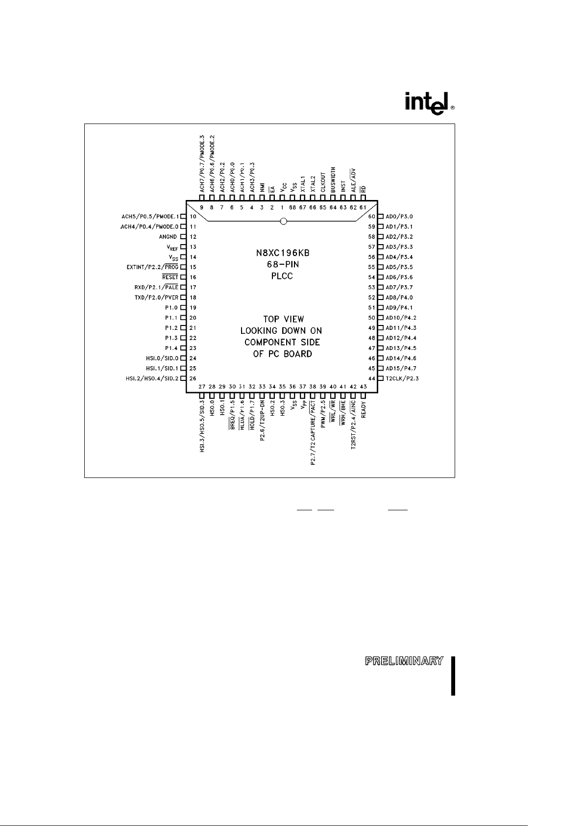
Figure 3. 68-Pin Package (PLCC Top View)
NOTE:
The above pin out diagram applies to the OTP (87C196KB) device. The OTP device uses all of the programming pins shown
above. The ROM (83C196KB) device only uses programming pins: AINC
, PALE, PMODE.n, and PROG. The ROMless
(80C196KB) doesn’t use any of the programming pins.
4
8XC196KB/8XC196KB16
270909– 4
NOTE:
N.C. means No Connect (do not connect these pins).
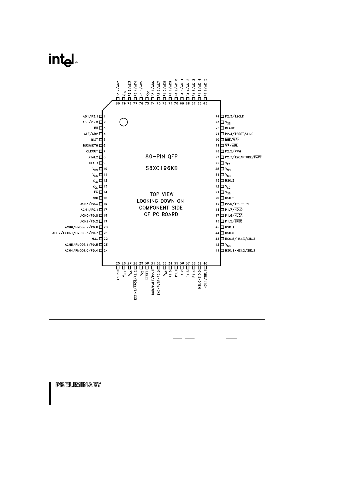
Figure 4. 80-Pin QFP Package
NOTE:
The above pin out diagram applies to the OTP (87C196KB) device. The OTP device uses all of the programming pins shown
above. The ROM (83C196KB) device only uses programming pins: AINC
, PALE, PMODE.n, and PROG. The ROMless
(80C196KB) doesn’t use any of the programming pins.
5
8XC196KB/8XC196KB16
PIN DESCRIPTIONS
Symbol Name and Function
V
CC
Main supply voltage (5V).
V
SS
Digital circuit ground (0V). There are multiple VSSpins, all of them must be connected.
V
REF
Reference voltage for the A/D converter (5V). V
REF
is also the supply voltage to the analog
portion of the A/D converter and the logic used to read Port 0. Must be connected for A/D
and Port 0 to function.
ANGND Reference ground for the A/D converter. Must be held at nominally the same potential as
V
SS
. Connect VSSand ANGND at chip to avoid noise problems.
V
PP
Programming voltage. Also timing pin for the return from power down circuit.
XTAL1 Input of the oscillator inverter and of the internal clock generator.
XTAL2 Output of the oscillator inverter.
CLKOUT Output of the internal clock generator. The frequency of CLKOUT is (/2 the oscillator
frequency. It has a 50% duty cycle.
RESET Reset input to and open-drain output from the chip. Input low for at least 4 state times to reset
the chip. The subsequent low-to-high transition re-synchronizes CLKOUT and commences a
10-state-time RESET sequence.
BUSWIDTH Input for buswidth selection. If CCR bit 1 is a one, this pin selects the bus width for the bus
cycle in progress. If BUSWIDTH is a 1, a 16-bit bus cycle occurs. If BUSWIDTH isa0an8-bit
cycle occurs. If CCR bit 1 is a 0, the bus is always an 8-bit bus.
NMI A positive transition causes a vector through 203EH.
INST Output high during an external memory read indicates the read is an instruction fetch and
output low indicates a data fetch. INST is valid throughout the bus cycle. INST is activated
only during external memory accesses.
EA Input for memory select (External Access). EA equal to a TTL-high causes memory accesses
to locations 2000H through 3FFFH to be directed to on-chip ROM/OTPROM. EA equal to a
TTL-low causes accesses to these locations to be directed to off-chip memory.
ALE/ADV Address Latch Enable or Address Valid output, as selected by CCR. Both pin options provide
a latch to demultiplex the address from the address/data bus. When the pin is ADV
, it goes
inactive high at the end of the bus cycle. ALE/ADV
is activated only during external memory
accesses.
RD Read signal output to external memory. RD is activated only during external memory reads.
WR/WRL Write and Write Low output to external memory, as selected by the CCR. WR will go low for
every external write, while WRL
will go low only for external writes where an even byte is
being written. WR
/WRL is activated only during external memory writes.
BHE/WRH Bus High Enable or Write High output to external memory, as selected by the CCR. BHE will
go low for external writes to the high byte of the data bus. WRH
will go low for external writes
where an odd byte is being addressed. BHE
/WRH is activated only during external memory
writes.
READY Ready input to lengthen external memory cycles. If the pin is low prior to the falling edge of
CLKOUT, the memory controller goes into a wait mode until the next positive transition in
CLKOUT occurs with READY high. When the external memory is not being used, READY has
no effect. Internal control of the number of wait states inserted into a bus cycle (held not
ready) is available in the CCR.
HSI Inputs to High Speed Input Unit. Four HSI pins are available: HSI.0, HSI.1, HSI.2 and HSI.3.
Two of them (HSI.2 and HSI.3) are shared with the HSO Unit.
HSO Outputs from High Speed Output Unit. Six HSO pins are available: HSO.0, HSO.1, HSO.2,
HSO.3, HSO.4 and HSO.5. Two of them (HSO.4 and HSO.5) are shared with the HSI Unit.
6
8XC196KB/8XC196KB16
PIN DESCRIPTIONS (Continued)
Symbol Name and Function
Port 0 8-bit high impedance input-only port. Three pins can be used as digital inputs and/or as
analog inputs to the on-chip A/D converter.
Port 1 8-bit quasi-bidirectional I/O port. These pins are shared with HOLD, HLDA and BREQ
.
Port 2 8-bit multi-functional port. All of its pins are shared with other functions in the 87C196KB.
Pins P2.6 and P2.7 are quasi-bidirectional.
Ports 3 and 4 8-bit bidirectional I/O ports with open drain outputs. These pins are shared with the
multiplexed address/data bus, which has strong internal pullups.
HOLD Bus Hold input requesting control of the bus. Enabled by setting WSR.7.
HLDA Bus Hold acknowledge output indicating release of the bus. Enabled by setting WSR.7.
BREQ Bus Request output activated when the bus controller has a pending external memory
cycle. Enabled by setting WSR.7.
TxD The TxD pin is used for serial port transmission in Modes 1, 2 and 3. In Mode 0 the pin is
used as the serial clock output.
RxD Serial Port Receive pin used for serial port reception. In Mode 0 the pin functions as input or
output data.
EXTINT A rising edge on the EXTINT pin will generate an external interrupt.
T2CLK The T2CLK pin is the Timer2 clock input or the serial port baud rate generator input.
T2RST A rising edge on the T2RST pin will reset Timer2.
PWM The pulse width modulator output.
T2UP-DN The T2UPDN pin controls the direction of Timer2 as an up or down counter.
T2CAPTURE A rising edge on P2.7 will capture the value of Timer2 in the T2CAPTURE register.
PMODE Programming Mode Select. Determines the EPROM programming algorithm that is
performed. PMODE is sampled after a chip reset and should be static while the part is
operating.
SID Slave ID Number. Used to assign each slave a pin of Port 3 or 4 to use for passing
programming verification acknowledgement.
PALE Programming ALE Input. Accepted by the 87C196KB when it is in Slave Programming
Mode. Used to indicate that Ports 3 and 4 contain a command/address.
PROG Programming. Falling edge indicates valid data on PBUS and the beginning of
programming. Rising edge indicates end of programming.
PACT Programming Active. Used in the Auto Programming Mode to indicate when programming
activity is complete.
PVAL Program Valid. This signal indicates the success or failure of programming in the Auto
Programming Mode. A zero indicates successful programming.
PVER Program Verification. Used in Slave Programming and Auto CLB Programming Modes.
Signal is low after rising edge of PROG if the programming was not successful.
AINC Auto Increment. Active low signal indicates that the auto increment mode is enabled. Auto
Increment will allow reading or writing of sequential EPROM locations without address
transactions across the PBUS for each read or write.
Ports 3 Address/Command/Data Bus. Used to pass commands, addresses, and data to and from
slave mode 87C196KBs. Used by chips in Auto Programming Mode to pass command,
and 4
addresses and data to slaves. Also used in the Auto Programming Mode as a regular
(Programming
system bus to access external memory. Should have pullups to V
CC
when used in slave
Mode)
programming mode.
7

8XC196KB/8XC196KB16
ELECTRICAL CHARACTERISTICS
ABSOLUTE MAXIMUM RATINGS*
Ambient Temperature
Under Bias ААААААААААААААААА
b
55§Ctoa125§C
Storage Temperature ААААААААААb65§Ctoa150§C
Voltage On Any Pin to V
SS
ААААААААb0.5V toa7.0V
Power Dissipation
(1)
ААААААААААААААААААААААА1.5W
NOTE:
1. Power dissipation is based on package heat transfer limitations, not device power consumption.
NOTICE: This data sheet contains preliminary information on new products in production. The specifications are subject to change without notice. Verify with
your local Intel Sales office that you have the latest
data sheet before finalizing a design.
*
WARNING: Stressing the device beyond the ‘‘Absolute
Maximum Ratings’’ may cause permanent damage.
These are stress ratings only. Operation beyond the
‘‘Operating Conditions’’ is not recommended and extended exposure beyond the ‘‘Operating Conditions’’
may affect device reliability.
OPERATING CONDITIONS
(All characteristics in this data sheet apply to these operating conditions unless otherwise noted.)
Symbol Description Min Max Units
T
A
Ambient Temperature Under Bias 0
a
70
§
C
V
CC
Digital Supply Voltage 4.50 5.50 V
V
REF
Analog Supply Voltage 4.50 5.50 V
F
OSC
Oscillator Frequency 12 MHz 3.5 12 MHz
F
OSC
Oscillator Frequency 16 MHz 3.5 16 MHz
NOTE:
ANGND and V
SS
should be nominally at the same potential.
DC CHARACTERISTICS
Symbol Description Min Max Units Test Conditions
V
IL
Input Low Voltage
b
0.5 0.8 V
V
IH
Input High Voltage (All Pins except 0.2 V
CC
a
0.9 V
CC
a
0.5 V
XTAL1 and RESET)
V
IH1
Input High Voltage on XTAL 1 0.7 V
CC
V
CC
a
0.5 V
V
IH2
Input High Voltage on RESET 2.6 V
CC
a
0.5 V
V
OL
Output Low Voltage 0.3 V I
OL
e
200 mA
0.45 V I
OL
e
3.2 mA
1.5 V I
OL
e
7mA
V
OH
Output High Voltage V
CC
b
0.3 V I
OH
eb
200 mA
(Standard Outputs)
(2)
V
CC
b
0.7 V I
OH
eb
3.2 mA
V
CC
b
1.5 V I
OH
eb
7mA
V
OH1
Output High Voltage V
CC
b
0.3 V I
OH
eb
10 mA
(Quasi-bidirectional Outputs)
(1)
V
CC
b
0.7 V I
OH
eb
30 mA
V
CC
b
1.5 V I
OH
eb
60 mA
I
LI
Input Leakage Current
g
10 mA0kV
IN
k
V
CC
b
0.3V
(Std. Inputs)
(3)
I
LI1
Input Leakage Current (Port 0)
a
3 mA0kV
IN
k
V
REF
I
TL
1 to 0 Transition Current
b
800 mAV
IN
e
2.0V
(QBD Pins)
(1)
I
IL
Logical 0 Input Current (QBD Pins)
(1)
b
50 mAV
IN
e
0.45V
8

8XC196KB/8XC196KB16
DC CHARACTERISTICS (Continued)
Symbol Description Min Typ
(7)
Max Units Test Conditions
I
IL1
Logical 0 Input Current in Reset
b
850 mAV
IN
e
0.45V
BHE
,WR, P2.0
I
IL2
Logical 0 Input Current in Reset
b
7mAV
IN
e
0.45V
ALE, RD
, INST
I
IH1
Logical 1 Input Current 100 mAV
IN
e
2.0V
on NMI Pin
Hyst. Hysteresis on RESET Pin 300 mV
I
CC
Active Mode Current in Reset 50 60 mA XTAL1e16 MHz
I
REF
A/D Converter Reference Current 2 5 mA
V
CC
e
V
PP
e
V
REF
e
5.5V
I
IDLE
Idle Mode Current 10 25 mA
I
PD
Powerdown Mode Current 5 30 mAV
CC
e
V
PP
e
V
REF
e
5.5V
R
RST
Reset Pullup Resistor 6K 50K X
C
S
Pin Capacitance (Any Pin to VSS)10pFF
TEST
e
1.0 MHz
NOTES: (Notes apply to all specifications)
1. QBD (Quasi-bidirectional) pins include Port 1, P2.6 and P2.7.
2. Standard Outputs include AD0 – 15, RD
,WR, ALE, BHE, INST, HSO pins, PWM/P2.5, CLKOUT, RESET, Ports 3 and 4,
TXD/P2.0 and RXD (in serial mode 0). The V
OH
specification is not valid for RESET. Ports 3 and 4 are open-drain outputs.
3. Standard Inputs include HSI pins, EA
, READY, BUSWIDTH, NMI, RXD/P2.1, EXTINT/P2.2, T2CLK/P2.3 and T2RST/
P2.4.
4. Maximum current per pin must be externally limited to the following values if V
OL
is held above 0.45V or VOHis held
below V
CC
b
0.7V:
I
OL
on Output pins: 10 mA
I
OH
on quasi-bidirectional pins: self limiting
I
OH
on Standard Output pins: 10 mA
5. Maximum current per bus pin (data and control) during normal operation is
g
3.2 mA.
6. During normal (non-transient) conditions the following total current limits apply:
Port 1, P2.6 I
OL
:29mA IOHis self limiting
HSO, P2.0, RXD, RESET
IOL:29mA IOH:26mA
P2.5, P2.7, WR
, BHE IOL:13mA IOH:11mA
AD0–AD15 I
OL
:52mA IOH:52mA
RD
, ALE, INST – CLKOUT IOL:13mA I
OH
:13mA
7. Typicals are based on a limited number of samples and are not guaranteed. The values listed are at room temperature
and V
REF
e
V
CC
e
5V.
ICCMaxe3.88cFREQa8.43 270909– 5
I
IDLE
Maxe1.65cFREQa2.2
Figure 6. ICCand I
IDLE
vs Frequency
9

8XC196KB/8XC196KB16
AC CHARACTERISTICS
Test Conditions: Capacitive load on all pinse100 pF, Rise and fall timese10 ns, F
OSC
e
12/16 MHz
The system must meet these specifications to work with the 87C196KB:
Symbol Description Min Max Units Notes
T
AVYV
Address Valid to READY Setup 2 T
OSC
b
75 ns
T
YLYH
NonREADY Time No upper limit ns
T
CLYX
READY Hold after CLKOUT Low 0 T
OSC
b
30 ns (Note 1)
T
LLYX
READY Hold after ALE Low T
OSC
b
15 2 T
OSC
b
40 ns (Note 1)
T
AVGV
Address Valid to Buswidth Setup 2 T
OSC
b
75 ns
T
CLGX
Buswidth Hold after CLKOUT Low 0 ns
T
AVDV
Address Valid to Input Data Valid 3 T
OSC
b
55 ns (Note 2)
T
RLDV
RD Active to Input Data Valid T
OSC
b
23 ns (Note 2)
T
CLDV
CLKOUT Low to Input Data Valid T
OSC
b
50 ns
T
RHDZ
End of RD to Input Data Float T
OSC
b
20 ns
T
RXDX
Data Hold after RD Inactive 0 ns
NOTES:
1. If max is exceeded, additional wait states will occur.
2. When using wait states, add 2 T
OSC
c
n where nenumber of wait states.
10
8XC196KB/8XC196KB16
AC CHARACTERISTICS (Continued)
Test Conditions: Capacitive load on all pins
e
100 pF, Rise and fall timese10 ns, F
OSC
e
12/16 MHz
The 87C196KB will meet these specifications:
Symbol Description Min Max Units Notes
F
XTAL
Frequency on XTAL1 12 MHz 3.5 12.0 MHz (Note 2)
F
XTAL
Frequency on XTAL1 16 MHz 3.5 16.0 MHz (Note 2)
T
OSC
1/F
XTAL
12 MHz 83.3 286 ns
T
OSC
1/F
XTAL
16 MHz 62.5 286 ns
T
XHCH
XTAL1 High to CLKOUT High or Low
a
20
a
110 ns
T
CLCL
CLKOUT Cycle Time 2 T
OSC
ns
T
CHCL
CLKOUT High Period T
OSC
b
10 T
OSC
a
10 ns
T
CLLH
CLKOUT Falling Edge to ALE Rising
b
10
a
10 ns
T
LLCH
ALE Falling Edge to CLKOUT Rising
b
15
a
15 ns
T
LHLH
ALE Cycle Time 4 T
OSC
ns (Note 3)
T
LHLL
ALE High Period T
OSC
b
10 T
OSC
a
10 ns
T
AVLL
Address Setup to ALE Falling Edge T
OSC
b
20 ns
T
LLAX
Address Hold after ALE Falling Edge T
OSC
b
40 ns
T
LLRL
ALE Falling Edge to RD Falling Edge T
OSC
b
35 ns
T
RLCL
RD Low to CLKOUT Falling Edge
a
4
a
25 ns
T
RLRH
RD Low Period T
OSC
b
5T
OSC
a
25 ns (Note 3)
T
RHLH
RD Rising Edge to ALE Rising Edge T
OSC
T
OSC
a
25 ns (Note 1)
T
RLAZ
RD Low to Address Float
a
5ns
T
LLWL
ALE Falling Edge to WR Falling Edge T
OSC
b
10 ns
T
CLWL
CLKOUT Low to WR Falling Edge 0
a
25 ns
T
QVWH
Data Stable to WR Rising Edge T
OSC
b
23 ns (Note 3)
T
CHWH
CLKOUT High to WR Rising Edge
b
5
a
15 ns
T
WLWH
WR Low Period T
OSC
b
15 T
OSC
a
5 ns (Note 3)
T
WHQX
Data Hold after WR Rising Edge T
OSC
b
15 ns
T
WHLH
WR Rising Edge to ALE Rising Edge T
OSC
b
15 T
OSC
a
10 ns (Note 1)
T
WHBX
BHE, INST HOLD after WR Rising Edge T
OSC
b
15 ns
T
RHBX
BHE, INST HOLD after RD Rising Edge T
OSC
b
10 ns
T
WHAX
AD8–15 hold after WR Rising Edge T
OSC
b
30 ns
T
RHAX
AD8–15 hold after RD Rising Edge T
OSC
b
25 ns
NOTES:
1. Assuming back-to-back bus cycles.
2. Testing performed at 3.5 MHz, however, the device is static by design and will typically operate below 1 Hz.
3. When using wait states, all 2 T
OSC
a
n where nenumber of wait states.
11

8XC196KB/8XC196KB16
System Bus Timings
270909– 6
12

8XC196KB/8XC196KB16
READY Timings (One Wait State)
270909– 7
Buswidth Bus Timings
270909– 8
13

8XC196KB/8XC196KB16
HOLD/HLDA Timings
Symbol Description Min Max Units Notes
T
HVCH
HOLD Setup 55 ns (Note 1)
T
CLHAL
CLKOUT Low to HLDA Low 15 ns
T
CLBRL
CLKOUT Low to BREQ Low 15 ns
T
HALAZ
HLDA Low to Address Float 10 ns
T
HALBZ
HLDA Low to BHE, INST, RD,WRFloat 10 ns
T
CLHAH
CLKOUT Low to HLDA High
b
15 15 ns
T
CLBRH
CLKOUT Low to BREQ High
b
15 15 ns
T
HAHAX
HLDA High to Address No Longer Float
b
15 ns
T
HAHAV
HLDA High to Address Valid 0 ns
T
HAHBX
HLDA High to BHE, INST, RD,WRNo Longer Float
b
20 ns
T
HAHBV
HLDA High to BHE, INST, RD,WRValid 0 ns
T
CLLH
CLKOUT Low to ALE High
b
515 ns
NOTE:
1. To guarantee recognition at next clock.
Maximum Hold Latency
Bus Cycle Type Latency
Internal Access 1.5 States
16-Bit External Execution 2.5 States
8-Bit External 4.5 States
270909– 9
14

8XC196KB/8XC196KB16
EXTERNAL CLOCK DRIVE
Symbol Parameter Min Max Units
1/T
XLXL
Oscillator Frequency 12 MHz 3.5 12.0 MHz
1/T
XLXL
Oscillator Frequency 16 MHz 3.5 16 MHz
T
XLXL
Oscillator Period 12 MHz 83.3 286 ns
T
XLXL
Oscillator Period 16 MHz 62.5 286 ns
T
XHXX
High Time 21.25 ns
T
XLXX
Low Time 21.25 ns
T
XLXH
Rise Time 10 ns
T
XHXL
Fall Time 10 ns
EXTERNAL CLOCK DRIVE WAVEFORMS
270909– 10
An external oscillator may encounter as much as a 100 pF load at XTAL1 when it starts-up. This is due to
interaction between the amplifier and its feedback capacitance. Once the external signal meets the V
IL
and
V
IH
specifications, the capacitance will not exceed 20 pF.
EXTERNAL CRYSTAL CONNECTIONS
270909– 11
NOTE:
Keep oscillator components close to chip and use
short, direct traces to XTAL1, XTAL2 and V
SS
. When
using crystals, C1
e
20 pF, C2e20 pF. When using
ceramic resonators, consult manufacturer for recommended circuitry.
EXTERNAL CLOCK CONNECTIONS
270909– 12
* Required if open-collector TTL driver used
Not needed if CMOS driver is used.
AC TESTING INPUT, OUTPUT WAVEFORMS
270909– 13
AC Testing inputs are driven at 2.4V for a Logic ‘‘1’’ and 0.45V for
a Logic ‘‘0’’ Timing measurements are made at 2.0V for a Logic
‘‘1’’ and 0.8V for a Logic ‘‘0’’.
FLOAT WAVEFORMS
270909– 14
For Timing Purposes a Port Pin is no Longer Floating when a
200 mV change from Load Voltage Occurs and Begins to Float
when a 200 mV change from the Loaded V
OH/VOL
Level occurs;
I
OL/IOH
e
g
15 mA.
15
8XC196KB/8XC196KB16
EXPLANATION OF AC SYMBOLS
Each symbol is two pairs of letters prefixed by ‘‘T’’ for time. The characters in a pair indicate a signal and its
condition, respectively. Symbols represent the time between the two signal/condition points.
Conditions:
Signals:
H - High
L - Low
V - Valid
X - No Longer Valid
Z - Floating
A - Address
B - BHE
BR - BREQ
C - CLKOUT
D - DATA IN
G - Buswidth
H - HOLD
HA - HLDA
L - ALE/ADV
Q - DATA OUT
R-RD
W-WR/WRH/WRL
X - XTAL1
Y - READY
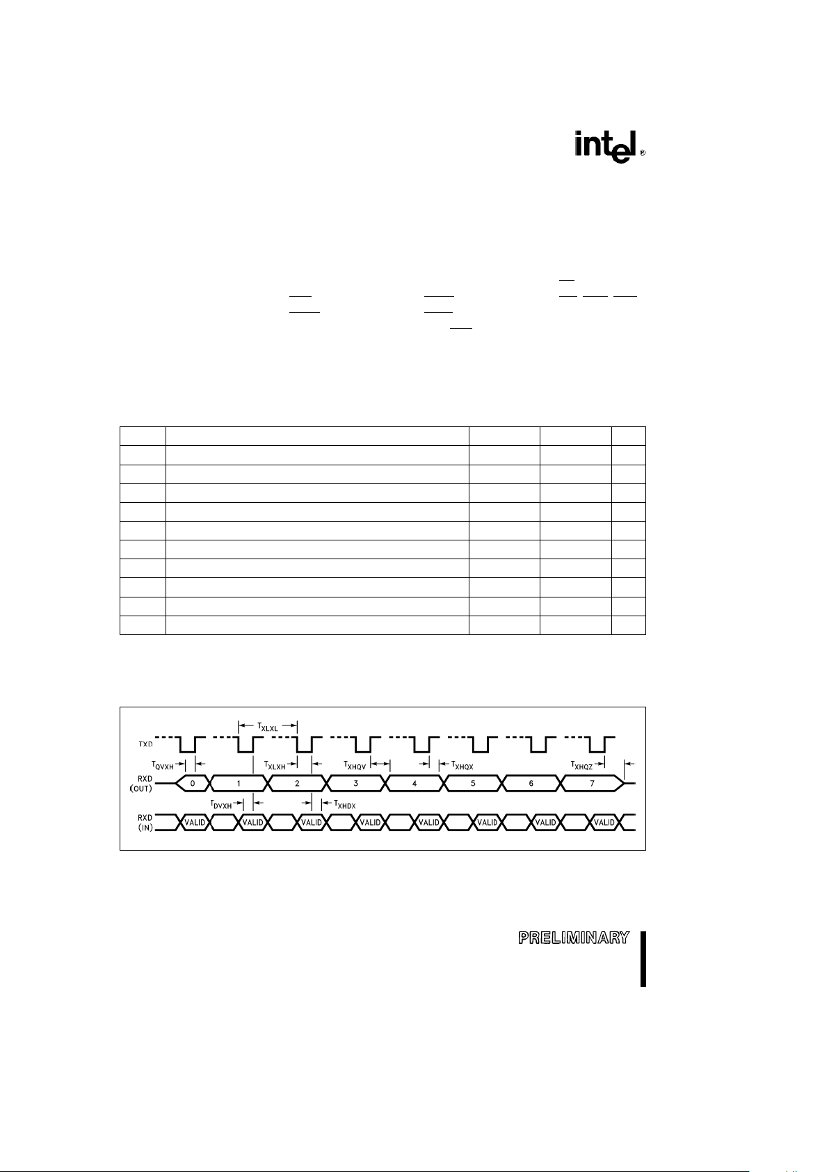
AC CHARACTERISTICSÐSERIAL PORTÐSHIFT REGISTER MODE
SERIAL PORT TIMINGÐSHIFT REGISTER MODE (MODE 0)
Symbol Parameter Min Max Units
T
XLXL
Serial Port Clock Period (BRRt8002H) 6 T
OSC
ns
T
XLXH
Serial Port Clock Falling Edge to Rising Edge (BRRt8002H) 4 T
OSC
b
50 4 T
OSC
a
50 ns
T
XLXL
Serial Port Clock Period (BRRe8001H) 4 T
OSC
ns
T
XLXH
Serial Port Clock Falling Edge to Rising Edge (BRRe8001H) 2 T
OSC
b
50 2 T
OSC
a
50 ns
T
QVXH
Output Data Setup to Clock Rising Edge 2 T
OSC
b
50 ns
T
XHQX
Output Data Hold after Clock Rising Edge 2 T
OSC
b
50 ns
T
XHQV
Next Output Data Valid after Clock Rising Edge 2 T
OSC
a
50 ns
T
DVXH
Input Data Setup to Clock Rising Edge T
OSC
a
50 ns
T
XHDX
Input Data Hold after Clock Rising Edge 0 ns
T
XHQZ
Last Clock Rising to Output Float 2 T
OSC
ns
WAVEFORMÐSERIAL PORTÐSHIFT REGISTER MODE
SERIAL PORT WAVEFORMÐSHIFT REGISTER MODE (MODE 0)
270909– 18
16

8XC196KB/8XC196KB16
10-BIT A/D CHARACTERISTICS
At a clock speed of 6 MHz or less, the clock prescaler should be disabled. This is accomplished by setting IOC2.4
e
1.
At higher frequencies (greater than 6 MHz) the clock
prescaler should be enabled (IOC2.4
e
0) to allow
the comparator to settle.
The table below shows two different clock speeds
and their corresponding A/D conversion and sample
times.
State times are calculated as follows:
state time
e
2
XTAL1
The converter is ratiometric, so the absolute accuracy is directly dependent on the accuracy and stability
of V
REF.VREF
must be close to VCCsince it supplies
both the resistor ladder and the digital section of the
converter.
See the MCS-96 A/D Converter Quick Reference
for definition of A/D terms.
Example Sample and Conversion Times
Sample Time
Conversion
Conversion
A/D Clock Clock Speed Sample Time at Clock
Time
Time at
Prescaler (MHz) (States) Speed
(States)
Clock Speed
(ms) (ms)
IOC2.4e0xON 16 15 1.875 156.5 19.6
IOC2.4e1xOFF 6 8 2.667 89.5 29.8
A/D CONVERTER SPECIFICATIONS
Parameter Typical(1) Minimum Maximum Units* Notes
Resolution 1024 1024 Levels
10 10 Bits
Absolute Error 0
g
3 LSBs
Full Scale Error 0.25g0.50 LSBs
Zero Offset Error 0.25g0.50 LSBs
Non-Linearity Error 1.5g2.5 0
g
3 LSBs
Differential Non-Linearity Error
l
b
1
a
2 LSBs
Channel-to-Channel Matching
g
0.1 0
g
1 LSBs
Repeatability
g
0.25 LSBs
Temperature Coefficients:
Offset 0.009 LSB/§C
Full Scale 0.009 LSB/
§
C
Differential Non-Linearity 0.009 LSB/
§
C
Off Isolation
b
60 dB 2, 3
Feedthrough
b
60 dB 2
VCCPower Supply Rejection
b
60 dB 2
Input Series Resistance 750 1.2K X 4
DC Input Leakage 0
g
3.0 mA
Sampling Capacitor 3 pF
NOTES:
*An ‘‘LSB’’, as used here, has a value of approximately 5 mV.
1. Typical values are expected for most devices at 25
§
C.
2. DC to 100 KHz.
3. Multiplexer Break-Before-Make Guaranteed.
4. Resistance from device pin, through internal MUX, to sample capacitor.
17

8XC196KB/8XC196KB16
OTPROM SPECIFICATIONS
OTPROM PROGRAMMING OPERATING CONDITIONS
Symbol Parameter Min Max Units
T
A
Ambient Temperature During Programming 20 30 C
VCC,VPD,V
REF
(1)
Supply Voltages During Programming 4.5 5.5 V
V
EA
Programming Mode Supply Voltage 12.50 13.0 V
(2)
V
PP
EPROM Programming Supply Voltage 12.50 13.0 V
(2)
VSS, ANGND
(3)
Digital and Analog Ground 0 0 V
F
OSC
Oscillator Frequency 12 MHz 6.0 12.0 MHz
F
OSC
Oscillator Frequency 16 MHz 6.0 16.0 MHz
NOTES:
1. V
CC,VPD
and V
REF
should nominally be at the same voltage during programming.
2. V
EA
and VPPmust never exceed the maximum voltage for any amount of time or the device may be damaged.
3. V
SS
and ANGND should nominally be at the same voltage (0V) during programming.
AC OTPROM PROGRAMMING CHARACTERISTICS
Symbol Description Min Max Units
T
SHLL
Reset High to First PALE Low 1100 T
OSC
T
LLLH
PALE Pulse Width 40 T
OSC
T
AVLL
Address Setup Time 0 T
OSC
T
LLAX
Address Hold Time 50 T
OSC
T
LLVL
PALE Low to PVER Low 60 T
OSC
T
PLDV
PROG Low to Word Dump Valid 50 T
OSC
T
PHDX
Word Dump Data Hold 50 T
OSC
T
DVPL
Data Setup Time 0 T
OSC
T
PLDX
Data Hold Time 50 T
OSC
T
PLPH
PROG Pulse Width 40 T
OSC
T
PHLL
PROG High to Next PALE Low 120 T
OSC
T
LHPL
PALE High to PROG Low 220 T
OSC
T
PHPL
PROG High to Next PROG Low 120 T
OSC
T
PHIL
PROG High to AINC Low 0 T
OSC
T
ILIH
AINC Pulse Width 40 T
OSC
T
ILVH
PVER Hold after AINC Low 50 T
OSC
T
ILPL
AINC Low to PROG Low 170 T
OSC
T
PHVL
PROG High to PVER Low 90 T
OSC
18

8XC196KB/8XC196KB16
DC OTPROM PROGRAMMING CHARACTERISTICS
Symbol Description Min Max Units
I
PP
VPPSupply Current (When Programming) 100 mA
NOTE:
Do not apply V
PP
until VCCis stable and within specifications and the oscillator/clock has stabilized or the device may be
damaged.
OTPROM PROGRAMMING WAVEFORMS
SLAVE PROGRAMMING MODE DATA PROGRAM MODE WITH SINGLE PROGRAM PULSE
270909– 15
SLAVE PROGRAMMING MODE IN WORD DUMP OR DATA VERIFY MODE WITH AUTO INCREMENT
270909– 16
19

8XC196KB/8XC196KB16
SLAVE PROGRAMMING MODE TIMING IN DATA PROGRAM MODE WITH REPEATED PROG PULSE
AND AUTO INCREMENT
270909– 17
20

8XC196KB/8XC196KB16
FUNCTIONAL DEVIATIONS
Devices marked with an ‘‘E’’, ‘‘F’’ or ‘‘G’’ have the
following errata.
1. Missed Interrupt on P0.7, EXTINT
Interrupts occurring on P0.7 could be missed since
the INTÐPEND EXTINT bit may not be set. See
techbit MC0893.
2. HSIÐMODE Divide-by-Eight
See Faxback
Ý
2192
REVISION HISTORY
This data sheet (270909-006) is valid for devices
with an ‘‘E’’, ‘‘F’’ or ‘‘G’’ at the end of the top side
tracking number. Data sheets are changed as new
device information becomes available. Verify with
your local Intel sales office that you have the latest
version before finalizing a design or ordering devices.
The following differences exist between this data
sheet (270909-006) and (270909-005):
1. Removed ‘‘Word Addressable Only’’ from Port 3
and 4 in Table 2.
2. Removed ICC1, active mode current at 3.5 MHz.
This specification is not longer required.
3. Removed TLLYV and TLLGV from waveform diagrams.
4. The HSI errata and CMPL with R0 were removed
as this is now considered normal operation.
5. The HSIÐMODE divide-by-eight errata was added to the known errata section.
The following differences exist between this data
sheet (270909-005) and (270909-004):
1. I
TL
MAX wasb650 mA (270909-004). Now I
TL
MAX isb800 mA (270909-005).
2. I
IL2
was named I
IL1
(270909-004). Now I
IL2
is
correctly named (270909-005).
3. I
IL1
was omitted (270909-004). I
IL1
MAX was
added. I
IL1
MAX isb850 mA (270909-005).
4. T
LLYV
and T
LLGV
(270909-004) were removed.
These timings are not required in high-speed system designs.
5. An errata was added to the known errata section.
There is a possibility to miss an external interrupt
on P0.7 EXTINT.
The following differences exist between this data
sheet (270909-004) and (270909-003):
1. The ROM (80C196KB), and ROMless
(83C196KB) were combined with this data sheet
resulting in no specification differences.
2. The description of the prescalar bit for the A/D
has been enhanced.
3. T
HAHBV
MIN wasb15 ns (270909-003). Now
T
HAHBV
MIN isb20 ns (270909-004).
4. T
XHQZ
MAX was 1 TOSC (270909-003). Now
T
XHQZ
MAX is 2 TOSC (270909-004). This should
have no impact on designs using synchronous
serial mode 0.
5. The change indicators for the 80C196KB are
‘‘E’’, ‘‘F’’ and ‘‘G’’. Previously there was only one
change indicator ‘‘E’’. The change indicator is
used for tracking purposes. The change indicator
is the last character in the FPO number. The FPO
number is the second line on the top side of the
device.
21

8XC196KB/8XC196KB16
The following differences exist between (-003) and
version (-002).
1. The 12 MHz and 16 MHz devices were combined in this data sheet. The 87C196KB 12 MHz
only data sheet (272035-001) is now obsolete.
2. Changes were made to the format of the data
sheet and the SFR descriptions were removed.
3. The -002 version of this data sheet was valid for
devices marked with a ‘‘B’’ or a ‘‘D’’ at the end
of the top side tracking number.
4. The OSCILLATOR errata was removed.
5. An errata was not documented in the -002 data
sheet for devices marked with a ‘‘B’’ or a ‘‘D’’.
This is the DIVIDE DURING HOLD/READY errata. When HOLD or READY is active and DIV/
DIVB is the last instruction in the queue, the divide result may be incorrect.
6. T
XCH
was changed from Mine40 ns to Min
e
20 ns.
7. T
RLCL
was changed from Mine5nstoMin
e
4 ns.
9. I
IL1
was changed from Max
eb
6mAtoMax
e
b
7 mA.
10. T
HAHBV
was changed from Min
eb
10 ns to
Min
eb
15 ns.
Differences between the -002 and -001 data sheets.
1. The -001 version of this data sheet was valid for
devices marked with a ‘‘C’’ at the end of the top
side tracking number.
2. Added 64L SDIP and 80L QFP packages.
3. Added IIH1.
4. Changed T
CHWH
Min fromb10 ns tob5 ns.
5. Changed T
CHWH
Max froma10 ns toa15 ns.
6. Changed T
WLWH
Min from T
OSC
b
20 ns to
T
OSC
b
15 ns.
7. Changed T
WHQX
Min from T
OSC
b
10 ns to
T
OSC
b
15 ns.
8. Changed T
WHLH
Min from T
OSC
b
10 ns to
T
OSC
b
15 ns.
9. Changed T
WHLH
Max from T
OSC
a
15 ns to
T
OSC
a
10 ns.
10. Changed T
WHBX
Min from T
OSC
b
10 ns to
T
OSC
b
15 ns.
11. Changed T
HVCH
Min from 85 ns to 55 ns.
12. Remove T
HVCH
Max.
13. Changed T
CLHAL
Min fromb10 ns tob15 ns.
14. Changed T
CLHAL
Max from 20 ns to 15 ns.
15. Changed T
CLBRL
Min fromb10 ns tob15 ns.
16. Changed T
CLBRL
Max from 20 ns to 15 ns.
17. Changed T
HAHAX
Min fromb10 ns tob15 ns.
18. Added HSI description to Functional Deviations.
19. Added Oscillator description to Functional Deviations.
22
 Loading...