*Other brands and names are the property of their respective owners.
Information in this document is provided in connection with Intel products. Intel assumes no liability whatsoever, including infringement of any patent or
copyright, for sale and use of Intel products except as provided in Intel’s Terms and Conditions of Sale for such products. Intel retains the right to make
changes to these specifications at any time, without notice. Microcomputer Products may have minor variations to this specification known as errata.
March 1996COPYRIGHT©INTEL CORPORATION, 1996 Order Number: 272814-001
8XC151SA/SB
HIGH-PERFORMANCE
CHMOS MICROCONTROLLER
Commercial/Express
Y
MCSÉ51 Microcontroller Compatible
Instruction Set
Y
Pin Compatible with 44-lead PLCC and
40-lead PDIP MCS 51 Sockets
Y
Fast Instruction Pipeline
Y
16-bit Internal Code Fetch
Y
8-bit, Min 2-clock External Code Fetch
in Page Mode
Y
User-selectable Configurations:
Ð External Wait States (0-3 wait states)
Ð Page Mode
Y
64K External Code Memory Space
Y
64K External Data Memory Space
Y
ROM/OTPROM Options:
8 Kbytes (SA), 16 Kbytes (SB)
or without ROM/OTPROM
Y
256 Bytes On-Chip RAM
Y
Power Management
Ð Idle Mode
Ð Powerdown Mode
Y
32 Programmable I/O Lines
Y
Seven Maskable Interrupt Sources with
Four Programmable Priority Levels
Y
Three Flexible 16-bit Timer/counters
Y
Hardware Watchdog Timer
Y
Programmable Counter Array
Ð High-speed Output
Ð Compare/Capture Operation
Ð Pulse Width Modulator
Ð Watchdog Timer
Y
Programmable Serial I/O Port
Ð Framing Error Detection
Ð Automatic Address Recognition
Y
High-performance CHMOS Technology
Y
Static Standby to 16-MHz Operation
Y
Package Options (PDIP, PLCC)
The 8XC151SA/SB has an MCS 51 microcontroller compatible instructon set. It is available in 40-pin PDIP and
44-lead PLCC compatible with the MCS 51 microcontroller. The 8XC151SA/SB has 256 bytes of on-chip RAM
and is available in 8/16 Kbytes of on-chip ROM/OTPROM or without ROM/OTPR OM. A variety of new
features such as programmable wait states, page mode and extended ALE can be selected using the new
user-programmable configuration.

8XC151SA/SB HIGH-PERFORMANCE CHMOS MICROCONTROLLER
272814–1
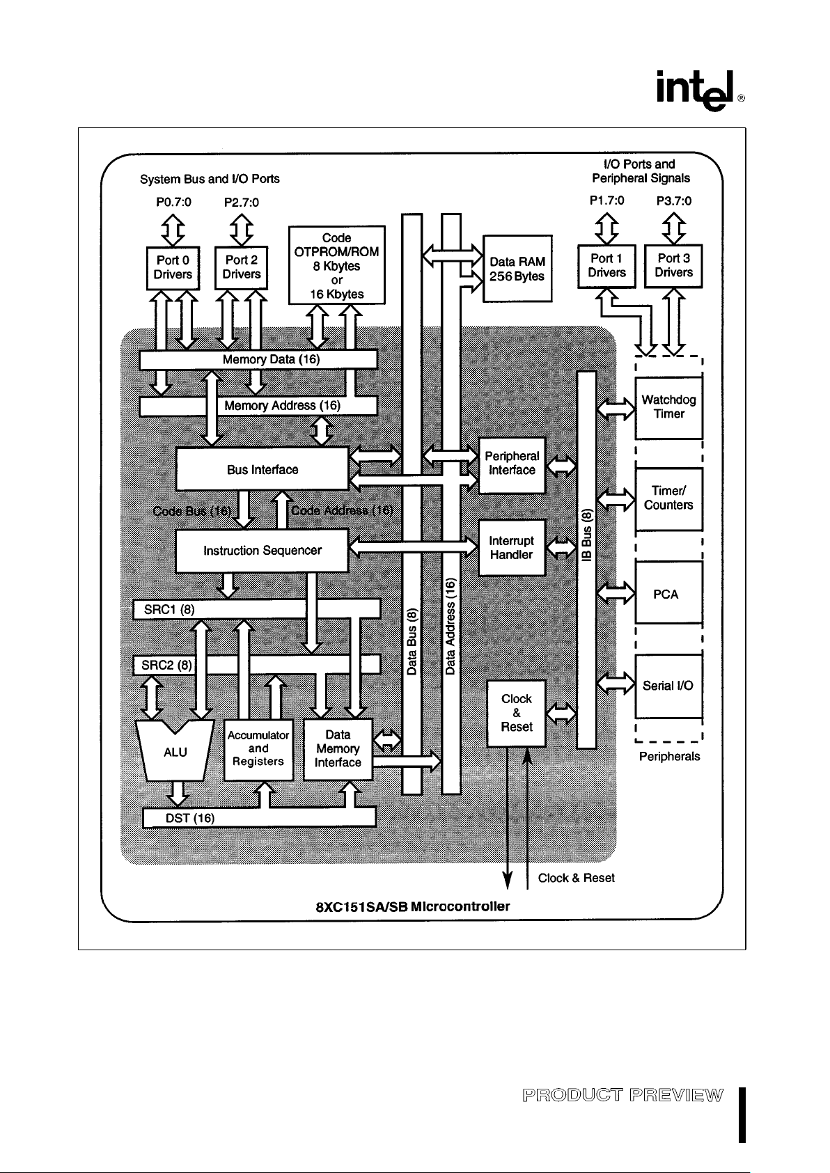
Figure 1. 8XC151SA/SB Block Diagram
2

8XC151SA/SB HIGH-PERFORMANCE CHMOS MICROCONTROLLER
TEMPERATURE RANGE
With the commercial (standard) temperature option,
the device operates over the temperature range 0
§
C
to
a
70§C. The express temperature option provides
b
40§Ctoa85§C device operation.
PROLIFERATION OPTIONS
Table 1 lists the proliferation options. See Figure 2
for the 8XC151SA/SB family nomenclature.
Table 1. Proliferation Options
8XC151SA/SB
(0 MHz – 16 MHz; 5V
g
10%)
80C151SB CPU-only
83C151SA 8K ROM
83C151SB 16K ROM
87C151SA 8K OTPROM
87C151SB 16K OTPROM
PROCESS INFORMATION
This device is manufactured on a complimentary
high-performance metal-oxide semiconductor
(CHMOS) process. Additional process and reliability
information is available in Intel’s
Components Quali-
ty and Reliability Handbook
(order number 210997).
All thermal impedance data is approximate for static
air conditions at 1 watt of power dissipation. Values
change depending on operating conditions and application requirements. The Intel
Packaging Hand-
book
(order number 240800) describes Intel’s ther-
mal impedance test methodology.
Table 2. Thermal Characteristics
Package Type i
JA
i
JC
44-Lead PLCC 46§C/W 16§C/W
40-Pin PDIP 45§C/W 16§C/W
PACKAGE OPTIONS
Table 3 lists the 8XC151SA/SB packages.
Table 3. Package Information
Pkg. Definition Temperature
N 44-Lead PLCC 0§Ctoa70§C
P 40-Pin Plastic DIP 0§Ctoa70§C
TN 44-Lead PLCC
b
40§Ctoa85§C
TP 40-Pin Plastic DIP
b
40§Ctoa85§C
3

8XC151SA/SB HIGH-PERFORMANCE CHMOS MICROCONTROLLER
272814–2
Figure 2. The 8XC151SA/SB Family Nomenclature
Table 4. Description of Product Nomenclature
Parameter Options Description
Temperature and Burn-in no mark Commercial operating temperature range (0§Cto70§C) with Intel
standard burn-in.
Options
T Express operating temperature range (b40§Cto85§C) with Intel
standard burn-in.
Packaging Options N 44-lead Plastic Leaded Chip Carrier (PLCC)
P 40-pin Plastic Dual In-line Package (PDIP)
Program Memory 0 Without ROM/OTPROM
Options
3 ROM
7 User programmable OTPROM
Process Information C CHMOS
Product Family 151 8-bit controller architecture
Device Memory Options SA/SB 256 bytes RAM/8/16 Kbyte ROM/OTPROM or without ROM/
OTPROM
Device Speed 16 External clock frequency
4

8XC151SA/SB HIGH-PERFORMANCE CHMOS MICROCONTROLLER
272814–3
Figure 3. 8XC151SA/SB 44-Lead PLCC Package
5

8XC151SA/SB HIGH-PERFORMANCE CHMOS MICROCONTROLLER
272814–4
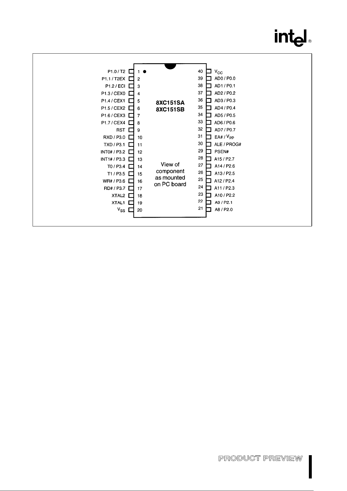
Figure 4. 8XC151SA/SB 40-Pin PDIP and Ceramic DIP Packages
6

8XC151SA/SB HIGH-PERFORMANCE CHMOS MICROCONTROLLER
Table 5. PLCC/DIP Signal Assignment Arranged by Functional Categories
Address & Data
Name PLCC DIP
AD0/P0.0 43 39
AD1/P0.1 42 38
AD2/P0.2 41 37
AD3/P0.3 40 36
AD4/P0.4 39 35
AD5/P0.5 38 34
AD6/P0.6 37 33
AD7/P0.7 36 32
A8/P2.0 24 21
A9/P2.1 25 22
A10/P2.2 26 23
A11/P2.3 27 24
A12/P2.4 28 25
A13/P2.5 29 26
A14/P2.6 30 27
A15/P2.7 31 28
Processsor Control
Name PLCC DIP
P3.2/INT0
Ý
14 12
P3.3/INT1
Ý
15 13
EAÝ/V
PP
35 31
RST 10 9
XTAL1 21 18
XTAL2 20 19
Input/Output
Name PLCC DIP
P1.0/T2 2 1
P1.1/T2EX 3 2
P1.2/ECI 4 3
P1.3/CEX0 5 4
P1.4/CEX1 6 5
P1.5/CEX2 7 6
P1.6/CEX3 8 7
P1.7/CEX4 9 8
P3.0/RXD 11 10
P3.1/TXD 13 11
P3.4/T0 16 14
P3.5/T1 17 15
Power & Ground
Name PLCC DIP
V
CC
44 40
V
CC2
12 Ð
V
SS
22 20
V
SS1
1Ð
V
SS2
23, 34 Ð
EAÝ/V
PP
35 31
Bus Control & Status
Name PLCC DIP
P3.6/WR
Ý
18 16
P3.7/RD
Ý
19 17
ALE/PROG
Ý
33 30
PSEN
Ý
32 29
7

8XC151SA/SB HIGH-PERFORMANCE CHMOS MICROCONTROLLER
Table 6. Signal Assignments Arranged by Package Number
PLCC DIP Name
1ÐV
SS1
2 1 P1.0/T2
3 2 P1.1/T2EX
4 3 P1.2/ECI
5 4 P1.3/CEX0
6 5 P1.4/CEX1
7 6 P1.5/CEX2
8 7 P1.6/CEX3
9 8 P1.7/CEX4
10 9 RST
11 10 P3.0/RXD
12 Ð V
CC2
13 11 P3.1/TXD
14 12 P3.2/INT0
Ý
15 13 P3.3/INT1
Ý
16 14 P3.4/T0
17 15 P3.5/T1
18 16 P3.6/WR
Ý
19 17 P3.7/RD
Ý
20 18 XTAL2
21 19 XTAL1
22 20 V
SS
PLCC DIP Name
23 Ð V
SS2
24 21 A8/P2.0
25 22 A9/P2.1
26 23 A10/P2.2
27 24 A11/P2.3
28 25 A12/P2.4
29 26 A13/P2.5
30 27 A14/P2.6
31 28 A15/P2.7
32 29 PSEN
Ý
33 30 ALE/PROG
Ý
34 Ð V
SS2
35 31 EAÝ/V
pp
36 32 AD7/P0.7
37 33 AD6/P0.6
38 34 AD5/P0.5
39 35 AD4/P0.4
40 36 AD3/P0.3
41 37 AD2/P0.2
42 38 AD1/P0.1
43 39 AD0/P0.0
44 40 V
CC
8

8XC151SA/SB HIGH-PERFORMANCE CHMOS MICROCONTROLLER
SIGNAL DESCRIPTIONS
Table 7. Signal Descriptions
Signal
Type Description
Multiplexed
Name With
A15:8
²
O Address Lines. Upper address lines for the external bus. P2.7:0
AD7:0
²
I/O Address/Data Lines. Multiplexed lower address lines and data lines P0.7:0
for external memory.
ALE O Address Latch Enable. ALE signals the start of an external bus PROG
Ý
cycle and indicates that valid address information is available on lines
A15:8 and AD7:0. An external latch can use ALE to demultiplex the
address from the address/data bus.
CEX4:0 I/O Programmable Counter Array (PCA) Input/Output Pins. These P1.6:3
are input signals for the PCA capture mode and output signals for the
P1.7
PCA compare mode and PCA PWM mode.
EA
Ý
I External Access. Directs program memory accesses to on-chip or V
PP
off-chip code memory. For EA
Ý
e
0, all program memory accesses
are off-chip. For EA
Ý
e
1, an access is to on-chip ROM/OTPROM if
the address is within the range of the on-chip ROM/OTPROM;
otherwise the access is off-chip. The value of EA
Ý
is latched at
reset. For devices without on-chip ROM/OTPROM, EA
Ý
must be
strapped to ground.
ECI I PCA External Clock Input. External clock input to the 16-bit PCA P1.2
timer.
INT1:0
Ý
I External Interrupts 0 and 1. These inputs set bits IE1:0 in the TCON P3.3:2
register. If bits IT1:0 in the TCON register are set, bits IE1:0 are set by
a falling edge on INT1
Ý
/INT0Ý. If bits INT1:0 are clear, bits IE1:0
are set by a low level on INT1:0
Ý
.
PROG
Ý
I Programming Pulse. The programming pulse is applied to this pin ALE
for programming the on-chip OTPROM.
P0.7:0 I/O Port 0. This is an 8-bit, open-drain, bidirectional I/O port. AD7:0
P1.0 I/O Port 1. This is an 8-bit, bidirectional I/O port with internal pullups. T2
P1.1 T2EX
P1.2 ECI
P1.7:3 CEX3:0
CEX4
P2.7:0 I/O Port 2. This is an 8-bit, bidirectional I/O port with internal pullups. A15:8
²
The descriptions of A15:8/P2.7:0 and AD7:0/P0.7:0 are for the nonpage-mode chip configuration (compatible with
44-lead PLCC and 40-pin DIP MCS 51 microcontrollers). If the chip is configured for page-mode operation, port 0 carries
the lower address bits (A7:0), and port 2 carries the upper address bits (A15:8) and the data (D7:0).
9

8XC151SA/SB HIGH-PERFORMANCE CHMOS MICROCONTROLLER
Table 7. Signal Descriptions (Continued)
Signal
Type Description
Multiplexed
Name With
P3.0 I/O Port 3. This is an 8-bit, bidirectional I/O port with internal pullups. RXD
P3.1 TXD
P3.3:2 INT1:0
Ý
P3.5:4 T1:0
P3.6 WR
Ý
P3.7 RD
Ý
PSEN
Ý
O Program Store Enable. Read signal output. This output is asserted Ð
for a memory address range that depends on bits RD0 and RD1 in
configuration byte UCONFIG0.
RD
Ý
O Read. Read signal output to external data memory. P3.7
RST I Reset. Reset input to the chip. Holding this pin high for 64 oscillator Ð
periods while the oscillator is running resets the device. The port pins
are driven to their reset conditions when a voltage greater than V
IH1
is
applied, whether or not the oscillator is running. This pin has an
internal pulldown resistor, which allows the device to be reset by
connecting a capacitor between this pin and V
CC
.
Asserting RST when the chip is in idle mode or powerdown mode
returns the chip to normal operation.
RXD I/O Receive Serial Data. RXD sends and receives data in serial I/O P3.0
mode 0 and receives data in serial I/O modes 1, 2, and 3.
T1:0 I Timer 1:0 External Clock Inputs. When timer 1:0 operates as a P3.5:4
counter, a falling edge on the T1:0 pin increments the count.
T2 I/O Timer 2 Clock Input/Output. For the timer 2 capture mode, this P1.0
signal is the external clock input. For the clock-out mode, it is the
timer 2 clock output.
T2EX I Timer 2 External Input. In timer 2 capture mode, a falling edge P1.1
initiates a capture of the timer 2 registers. In auto-reload mode, a
falling edge causes the timer 2 registers to be reloaded. In the updown counter mode, this signal determines the count direction:
1
e
up, 0edown.
TXD O Transmit Serial Data. TXD outputs the shift clock in serial I/O mode P3.1
0 and transmits serial data in serial I/O modes 1, 2, and 3.
V
CC
PWR Supply Voltage. Connect this pin to thea5V supply voltage. Ð
V
CC2
PWR Secondary Supply Voltage 2. This supply voltage connection is Ð
provided to reduce power supply noise. Connection of this pin to the
a
5V supply voltage is recommended. However, when using the
8XC151SA/SB as a pin-for-pin replacement for the 8XC51FX, V
SS2
can be unconnected without loss of compatibility. (Not available on
DIP)
V
PP
I Programming Supply Voltage. The programming supply voltage is EA
Ý
applied to this pin for programming the on-chip OTPROM.
²
The descriptions of A15:8/P2.7:0 and AD7:0/P0.7:0 are for the nonpage-mode chip configuration (compatible with
44-lead PLCC and 40-pin DIP MCS 51 microcontrollers). If the chip is configured for page-mode operation, port 0 carries
the lower address bits (A7:0), and port 2 carries the upper address bits (A15:8) and the data (D7:0).
10
 Loading...