

Intel Corporation N83930HF, N83930HE Datasheet

ADVANCE INFORMATION
COPYRIGHT © INTEL CORPORATION, 1997 May 1997 Order Numbe r: 272928-003
8x930Hx
UNIVERSAL SERIAL BUS HUB
PERIPHERAL CONTROLLER
■ USB Hub with One Upstream, One
Internal Downstream, and Three
External Downstream Ports on HD/HE
Parts or Four on HF/HG Parts
—Complete Univer sal S erial Bu s Spe ci-
fication 1.0 Compatibility
—Serves as both USB Hub and USB
Embedded Function (Internal Port)
■ USB Hub
—Connectivity Management
—Downstream Device
Connect/Disconnect Detection
— Power Management, Including
Suspend and Resume
— Bus Fault De tection and Recovery
—Full and Low Speed Downstream
Device Support
■ Output Pin for Port Power Switching
■ Input Pin for Overcurrent Detection
■ USB Embedded Function
—Supports Isochronous and
Non-isochronous Data
■ On-chip USB Transceivers
■ Serial Bus Interface Engine (SIE)
—Packet Decoding/Generation
—CRC Generation and Checking
— NRZI Encoding/Decoding and
Bit-stuffing
■ Hub FIFO Data Buffers
—One Pair of 16-byte Transmit and
Receive FIFOs
—One 1-byte Transmit Register
■ Embedded Function FIFO Data Buffers
—Three Pairs of 16-byte Transmit and
Receive FIFOs
—One Pair of Configurable Transmit
and Receive FIFOs (1 Kbyte total)
■ Automatic Transmit/Receive FIFO
Management
■ Three USB Interrupt Vectors
—Endpoint Transmit/Receive Done
—Start of Frame/Hub Endpoint Done
—Global Suspend/Resume
■ Low Clock Mode
■ User-selectable Configurations
—External Wait State
—External Address Range
—Page Mode
■ Real-time Wait Function
■ 256-Kbyte External Code/Data Memory
Space
■ On-chip ROM Options
—0, 8, or 16 Kbytes
■ 1024 bytes On-chip Data RAM
■ Four Input/Output Ports
■ Standard MCS® 51 UART
■ Power-saving Idle and Powerdown
Modes
■ Register-based MCS® 251 Architecture
■ Code-compatible with MCS 51 and
MCS 251 Microcontrollers
■ 12-MHz Crystal Operation
The 8x930Hx USB hub peripheral controller i s based on the MCS 251 microcontroller. It consists of standard
8XC251Sx peripherals plus a USB module. The USB module provides both USB hub
and USB embedded
function capabilities. The 8
x
930Hx supports USB hub functionality, embedded function, suspend/resume
modes, isochronous/non-isochronous transfers, and it is fully USB rev 1.0 specification compliant. The USB
module contains one internal and three (or four) external downstream ports and integrates the USB transceivers, serial bus interface engine (SIE), hub interface unit (HIU), function interface unit (FIU), and
transmit /receive FIFOs. The 8
x
930Hx uses the standard instruction set of t he MCS 251 architecture, which is
binary code compatible with the MCS
51 architecture.

Information in this document is provided in connection with Intel products. No license, express or implied, by estoppel or oth-
erwise, to any intellectual property rights is granted by this document. Except as provided in Intel’s Terms and Conditions of
Sale for such produc t s, Intel assu m es no liabili ty w hatsoever, and Intel d is c l ai m s any express or implie d warranty, re lating to
sale and/or use of Intel products including liability or warranties relating to fitness for a particular purpose, merchantability, or
infringement of any paten t , copyrig ht or other intellec t ual prope r ty right. I ntel prod ucts are no t intended f or us e in medical, life
saving, or life sustaining applications.
Intel retains the right to make changes to specifications and product descriptions at any time, without notice.
*Third-party brands and names are the property of their respective owners.
Contact your lo cal I nte l sa les of fi ce or you r dis tri but or to ob tai n the late st spe cif icat i ons an d bef ore pl ac in g your pro duct order.
Copies of documents which have an ordering number and are referenced in this document, or other Intel literature, may be
obtained from:
Intel Corporation
Literature Sales
P.O. Box 7641
Mt. Prospect, IL 60056-76 41
or call 1-800-548- 4725
COPYRIGHT © INTEL CORPORATION, 1997

iii
CONTENTS
1.0 About This Document.......................................................................................................... 1
1.1 Additional Information Sources ...................................................................................... 1
1.2 Electronic Information..................................................................................................... 1
1.3 Product Summary........................................................................................................... 2
2.0 Nomenclature Overview ...................................................................................................... 4
3.0 Pinout.................................................................................................................................. 6
4.0 Signals .............................................................................................................................. 12
5.0 Address Map... ........ ........ ......... ........ ......... ................................. ......... ........ ......... ........ ..... 16
6.0 Electrical Characteristics................................................................................................... 17
6.1 Operating Frequencies................................................................................................. 17
6.2 DC Characteristics........................................................................................................ 18
6.3 Explanation of Timing Symbols.................................................................................... 20
6.4 System Bus AC Characteristics.................................................................................... 21
6.4.1 System Bus Timing Diagrams ...............................................................................23
6.4.2 Real-time Wait State Function AC Characteristics ................................................27
6.4.3 Real-time Wait State Function Timing Diagrams ..................................................28
6.5 AC Characteristics — Synchronous Mode 0................................................................ 30
6.6 External Clock Drive..................................................................................................... 30
6.7 Testing Waveforms ...................................................................................................... 31
7.0 Thermal Characteristics .................................................................................................... 32
8.0 Design Considerations...................................................................................................... 32
8.1 External Bus Timing and Peripheral Timing Affected by PLLSEL2:0 Selection........... 32
8.2 Low Clock Mode Frequency......................................................................................... 32
8.3 Setting RXFFRC Bit Clears Only the Oldest Packet in the FIFO ................................. 32
8.4 Series Resistor Requirement for Impedance Matching................................................ 32
8.5 Pullup Resistor Requirement for 8x930Hx Hub devices............................................... 32
8.6 Powerdown Mode Cannot Be Invoked Before USB Suspend...................................... 32
8.7 Unused Downstream Ports........................................................................................... 33
9.0 8x930Hx Errata................................................................................................................. 33
10.0 Datasheet Revision History............................................................................................... 33

8x930Hx UNIVERSAL SERIAL BUS PERIPHERAL CONTROLLER
iv
Figures
1. 8x930Hx Block Diagram.......................................................................................................2
2. 8x930Hx USB Module Block Diagram..................................................................................3
3. Product Nomenclature .........................................................................................................4
4. 8x930HD/HE and 8x930HF/HG 68-pin PLCC Package.......................................................6
5. 8x930HD/HE and 8x930HF/HG 64-pin SDIP Package........................................................7
6. 8x930Hx Code Fetch, Nonpage Mode...............................................................................23
7. 8x930Hx Data Read, Nonpage Mode................................................................................24
8. 8x930Hx Data Write, Nonpage Mode.................................................................................24
9. 8x930Hx Code Fetch, Page Mode.....................................................................................25
10. 8x930Hx Data Read, Page Mode ......................................................................................26
11. 8x930Hx Data Write, Page Mode.......................................................................................26
12. External Code Fetch/Data Read (Nonpage Mode, Real-time Wait State) .........................28
13. External Data Write (Nonpage Mode, Real-time Wait State).............................................28
14. External Data Read (Page Mode, Real-time Wait State)...................................................29
15. External Data Write (Page Mode, Real-time Wait State) ...................................................29
16. Serial Port Waveform — Synchronous Mode 0..................................................................30
17. External Clock Drive Waveforms....................... ......... ........ ........ ......... ........ .......................30
18. AC Testing Input, Output Waveforms.................................................................................31
19. Float Waveforms................................................................................................................31
Tables
1. Related Documentation........................................................................................................1
2. Electronic Information ....................................... ......... ........ ........ ......... ........ ......... ................1
3. Description of Product Nomenclature................ ......... ................................. ......... ........ ........4
5. Downstream Port Allocation.............................. ......... ........ ........ ......... ........ ......... ........ ........5
4. Proliferation Options.............................................................................................................5
6. 68-pin PLCC Pin Assignment ...............................................................................................8
7. 64-pin SDIP Pin Assignment............................. ......... ........ ........ ......... ........ ......... ........ ........9
8. 68-pin PLCC Signal Assignments Arranged by Functional Category................................10
9. 64-pin SDIP Signal Assignments Arranged by Functional Category..................................11
10. Signal Description..............................................................................................................12
11. Memory Signal Selections (RD1:0) ...................................................................................15
12. 8x930Hx Address Map.......................................................................................................16
13. 8x930Hx Operating Frequency..........................................................................................17
14. DC Characteristics at Operating Conditions.......................................................................18
15. AC Timing Symbol Definitions............................................................................................20
16. AC Characteristics at Operating Conditions.......................................................................21
17. Real-time Wait State AC Timing Specifications.................................................................27
18. Serial Port Timing — Synchronous Mode 0.......................................................................30
19. External Clock Drive................................................... ........ ........ ......... ...............................31
20. Thermal Characteristics .....................................................................................................32
ADVANCE INFORMATION 1
8x930Hx UNIVERSAL SERIAL BUS PERIPHERAL CONTROLLER
1.0 ABOUT THIS DOCUMENT
This data sheet contains advanc e i n formation about
Intel’s 8
x
930Hx Universal Serial Bus hub peripheral
controller, based on the MCS® 251 peripheral
controller, which includes a functional overview,
mechanical data, targeted electrical specifications
(simulated), and bus functional waveforms. A
detailed functional description, other than
parametric performance, is published in the
8x930Ax, 8x930Hx Universal Serial Bus Micorcon-
troller Us er’ s Manual
(272949).
1.1 Additional Information Sources
Intel documentation i s available from your l ocal Intel
Sales Representativ e or Intel Lit erature Sale s.
Intel Corporation
Literature Sales
P.O. Box 7641
Mt. Prospect , IL 60056-7641
1-800-879-4683
1.2 Electronic Information
We offer a variety of technical and product information through the World Wide Web (see Table 2
for URL) and through FaxBack service which is an
on-demand publishing system that sends
documents to your fax machine. You can get
product announcements, change notifications,
product literature, device characteristics, design
recommendations, and quality and reliability information 24 hours a day, 7 days a week. Just dial the
telephone number and respond to the system
prompts.
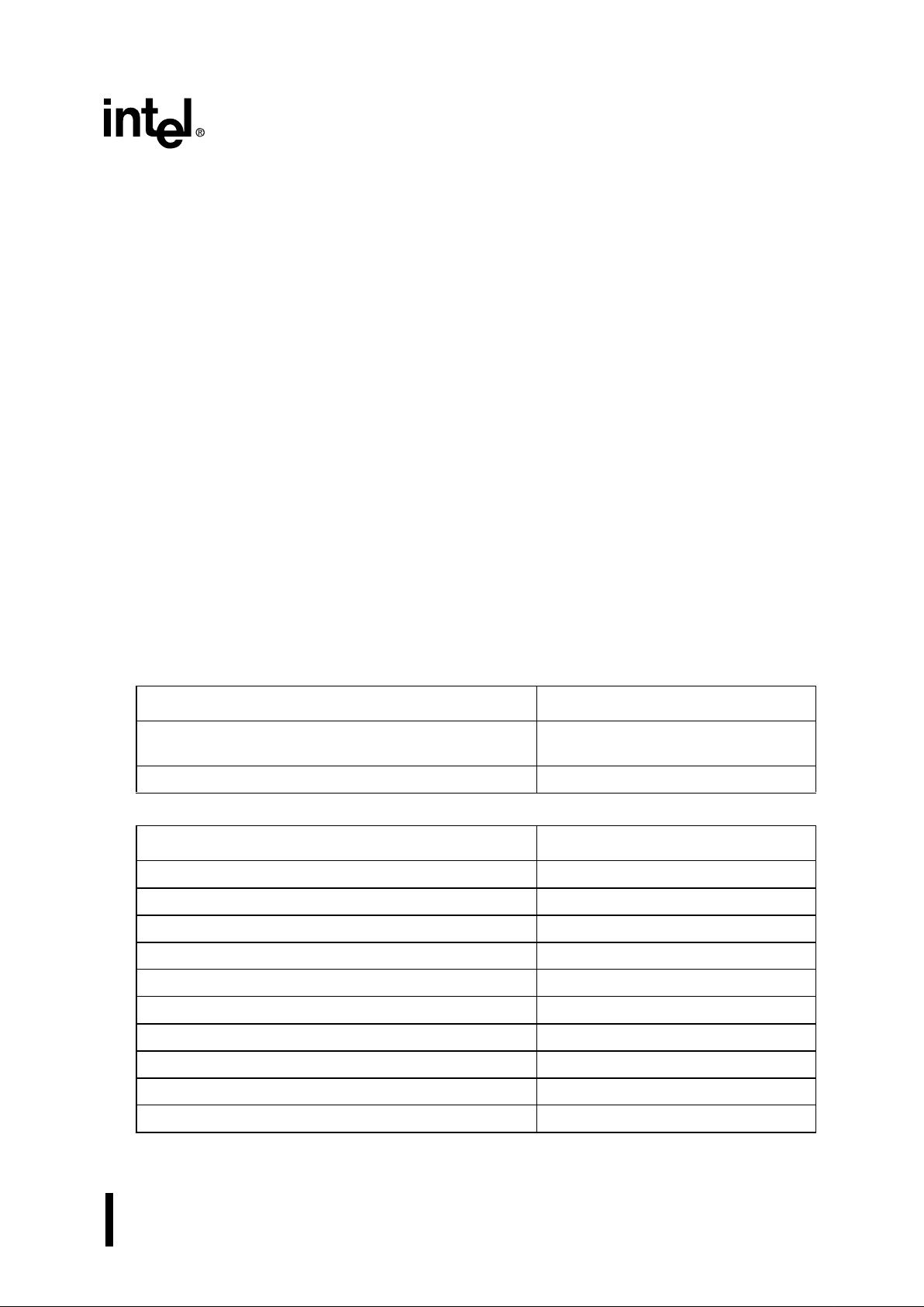
Table 1. Related Documentation
Table 2. Electronic Information
Document Title Order/Contact
8x930Ax, 8x930Hx Universal Serial Bus Micorcontroller
User’s Manual
Intel Order # 272949
Universal Serial Bus Specification
Intel Order # 272962
Document Title Order/Contact
Intel’s World-Wid e Web (WWW) Location: http://www.intel.com/design/usb/
Customer Support (US and Canada): 800-628-8686
FaxBack Servi ce:
US and Canada
800-628-228 3
Europe
+44(0)793-496646
worldwide
916-356-310 5
Application Bulletin Board Service:
up to 14.4-Kbaud line, worldwide
916-356-3600
dedicated 2400-baud lin e, worldwide
916-356-720 9
Europe
+44(0)793-496340
2 ADVANCE INFORMATION
8x930Hx UNIVERSAL SERIAL BUS PERIPHERAL CONTROLLER
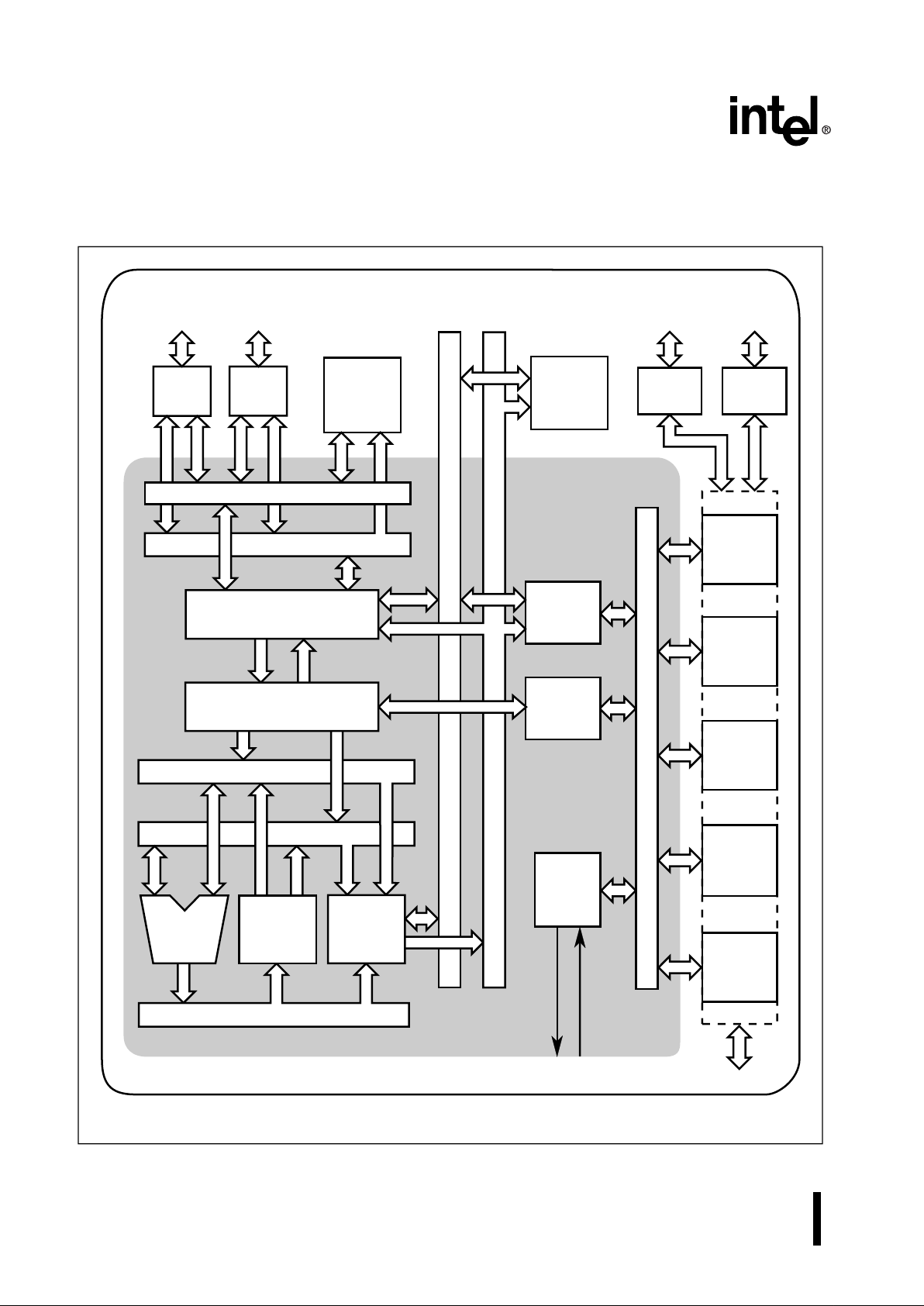
1.3 Product Summary
Figure 1. 8x930Hx Block Diagram
A4340-01
SRC2 (8)
Code Address (24)
Code Bus (16)
RAM
ROM
Watchdog
Timer
Timer/
Counters
PCA
Serial I/O
Port 2
Drivers
P2.7:0
Port 0
Drivers
P0.7:0
Port 3
Drivers
P3.7:0
Port 1
Drivers
P1.7:0
Data Address (24)
Data Bus (8)
Memory Address (16)
System Bus and I/O Ports
I/O Ports and
Peripheral Signals
SRC1 (8)
IB Bus (8)
Peripheral
Interface
Interrupt
Handler
Clock
&
Reset
Bus Interface
Instruction Sequencer
DST (16)
ALU
Data
Memory
Interface
Memory Data (16)
Register
File
USB
†
USB Ports
Microcontroller Core
†
For details, see the USB module block diagram.
ADVANCE INFORMATION 3
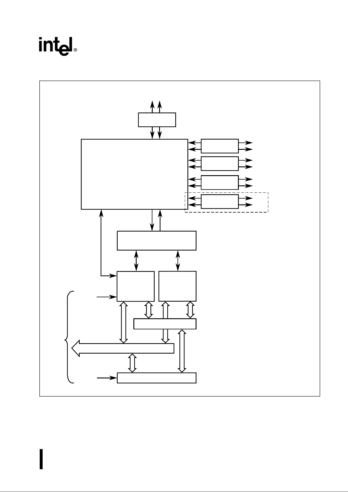
8x930Hx UNIVERSAL SERIAL BUS PERIPHERAL CONTROLLER
Figure 2. 8x930Hx USB Module Block Diagram
D
P3
D
M3
Transceiver
A5102-02
D
P5
D
M5
D
P2
D
M2
D
P1
DM0 D
P0
D
M1
Repeater
USB Upstream Port
USB
Downstream
Ports
Serial Bus Interface Engine
(SIE)
Transceiver
Transceiver
Transceiver
Hub
Interface
Unit
(HIU)
Function
Interface
Unit
(FIU)
Control
Control
FIFOs
Data Bus
To
CPU
Transmit/Receive Bus
Transceiver
HF/HG only
4 ADVANCE INFORMATION
8x930Hx UNIVERSAL SERIAL BUS PERIPHERAL CONTROLLER
2.0 NOMENCLATURE OVERVIEW
Figure 3. Product Nomenclature
Table 3. Description of Product Nomenclature
Parameter Options Description
Temperature and Burn-in no mark Commercial operating temperature range (0
o
C to 70oC) with
Intel standard burn-in
Packaging Op tions N Plastic Leaded Chip Carri er (PLCC)
U Shrink Dual In-Line Package (SDIP)
Program Memory Options 0 Without ROM
3 With ROM
Process and Voltage Information no mark CHMOS
Product Family 930Hx Advanced 8-bi t microcontroller archite ct ure with on-chip
Universal Serial Bus Hub and Function capability. Indicates
ROM size, RAM size, and quantity of external dow nstream
ports (see Table 4).
Device Speed no mark 12 MHz crystal
Program Memory Options
XXXXX XXXX8XXX
Packaging Options
Temperature and Burn-in Options
A2815-01
Process Information
Product Family
Device Speed
ADVANCE INFORMATION 5
8x930Hx UNIVERSAL SERIAL BUS PERIPHERAL CONTROLLER
Table 5. Downstream Port Allocation
Table 4. Proliferation Options
4 Extern a l
Downstream Ports
(HF/HG)
3 External
Downstream Ports
(HD/HE)
ROM Size RAM Size Package
N80930HF N80930HD 0 1024 bytes 68-pin PLCC
N83930HF N83930HD 8 Kbytes 1024 bytes 68-pin PLCC
N83930HG N83930HE 16 Kbytes 1024 bytes 68-pin PLCC
U80930HF U80930HD 0 1024 byte s 64-pin SDIP
U83930HF U83930HD 8 Kbytes 1024 bytes 64-pin SDIP
U83930HG U83930HE 16 Kbytes 1024 bytes 64-pin SDIP
Downstream Port
Number
8
x
930HD/HE 8x930HF/HG
1 External External
2 External External
3 External External
4 Internal ( Embedded Function) Internal (Embe dded Function)
5 — External
6 ADVANCE INFORMATION
8x930Hx UNIVERSAL SERIAL BUS PERIPHERAL CONTROLLER
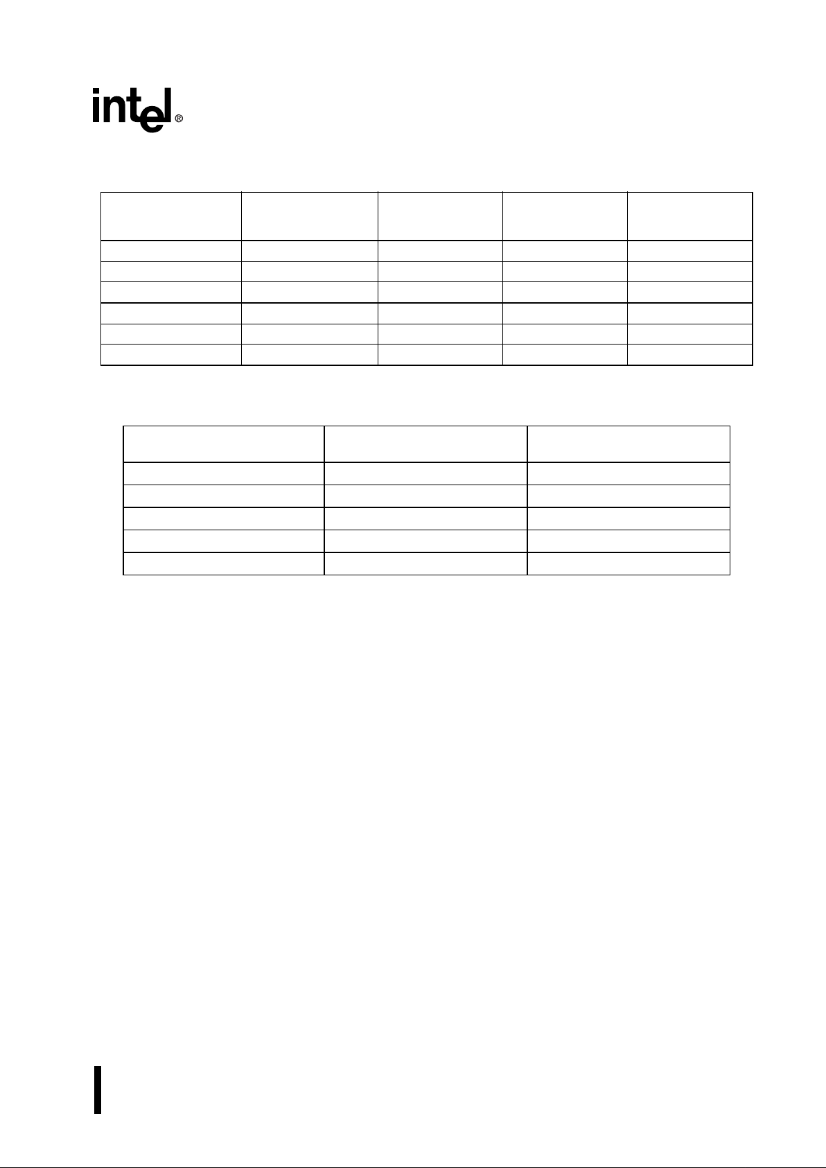
3.0 PINOUT
Figure 4 il l ustrates a di agram of the 8x930HD/HE PLCC package. T able 6 and T able 8 cont ai n indexes of the
pin arrangement. Table 10 contains the signal descriptions for all pins.
.
Figure 4. 8
x
930HD/HE and 8x930HF/HG 68-pin PLCC Package
UPWEN#†/
D
P5
†
OVRI#†/
D
M5
††
D
P1
D
M1
Reserved
D
P0
D
M0
ECAP
V
SSP
V
CCP
SOF#
D
P3
D
M3
Reserved
D
P2
D
M2
PLLSEL0
A8 / P2.0
A9 / P2.1
A10 / P2.2
A11 / P2.3
A12 / P2.4
A13 / P2.5
A14 / P2.6
A15 / P2.7
VSSVCCEA#
ALE
PSEN#
Reserved
Reserved
Reserved
†
/UPWEN#
††
Reserved
†
/OVRI#
††
A4421-01
AD7 / P0.7
AD6 / P0.6
AD5 / P0.5
AD4 / P0.4
AD3 / P0.3
AD2 / P0.2
AD1 / P0.1
AD0 / P0.0
V
SSP
V
CCP
P3.0 / RXD
P3.1 / TXD
P3.2 / INT0#
P3.3 / INT1#
P3.4 / T0
P3.5 / T1
P3.6 / WR#
60
59
58
57
56
55
54
53
52
51
50
49
48
47
46
45
44
View of component as
mounted on PC board
10
11
12
13
14
15
16
17
18
19
20
21
22
23
24
25
26
P3.7 / RD# / A16
P1.0 / T2
P1.1 / T2EX
P1.2 / ECI
P1.3 / CEX0
P1.4 / CEX1
P1.5 / CEX2
P1.6 / CEX3 / WAIT#
P1.7 / CEX4 / A17 / WCLK
V
CC
V
SS
XTAL1
XTAL2
AV
CC
RST
PLLSEL1
PLLSEL2
2728293031323334353637383940414243
987654321
68676665646362
61
NOTE:
Reserved pins must be left unconnected.
†
Specific to the 8x930HD/HE
††
Specific to the 8x930HF/HG
ADVANCE INFORMATION 7
8x930Hx UNIVERSAL SERIAL BUS PERIPHERAL CONTROLLER
Figure 5. 8x930HD/HE and 8x930HF/HG 64-pin SDIP Package
RESERVED†/
D
M5
††
AV
CC
AD2 / P0.2
P3.3 / INT1#
P3.2 / INT0#
AD3 / P0.3
AD1 / P0.1
P3.1 / TXD
AD0 / P0.0
P3.0 / RXD
ECAP
V
SSP
SOF#
V
CCP
DM0
PLLSEL0
DP0
PLLSEL2
DMI
PLLSEL1
DP1
RST
RESERVED†/
D
P5
††
XTAL2
OVRI#
XTAL1
UPWEN#
V
SS
PSEN#
V
CC
ALE
P1.7 / CEX4 / A17 / WCLK
EA#
P1.6 / CEX3 / WAIT#
V
CC
P1.5 / CEX2
V
SS
P1.4 / CEX1
A15 / P2.7
P1.3 / CEX0
A14 / P2.6
P1.2 / ECI
A13 / P2.5
P1.1 / T2EX
A12 / P2.4
P1.0 / T2
A11 / P2.3
P3.7 / A16 / RD#
A10 / P2.2
P3.6 / WR#
A9 / P2.1
P3.5 / T1
A8 / P2.0
P3.4 / T0
AD7 / P0.7
V
CCP
AD6 / P0.6
DP3
AD5 / P0.5
V
SSP
AD4 / P0.4
DM3
DP2
DM2
59
60
58
57
63
64
62
61
51
52
50
49
55
56
54
53
43
44
42
41
47
48
46
45
35
36
34
33
39
40
38
37
6
5
7
8
2
1
8X930HX
A4422-01
3
4
14
15
16
10
9
11
12
22
21
23
24
18
17
19
20
30
29
31
32
26
25
27
28
NOTE:
Reserved pins must be left unconnected.
56
View of
component
as mounted
on PC board
13
†
Specific to the 8x930HD/HE
††
Specific to the 8x930HF/HG
8 ADVANCE INFORMATION
8x930Hx UNIVERSAL SERIAL BUS PERIPHERAL CONTROLLER
Table 6. 68-pin PLCC Pin Assignment
Pin Name Pin Name Pin Name
1V
SS
24 P3.4/T0 47 Reserved
2 A15/P2.7 25 P3.5/T1 48 D
M3
3 A14/P2.6 26 P3.6/WR# 49 D
P3
4 A13/P2.5 27 P3.7/RD#/A16 50 SOF#
5 A12/P2.4 28 P1.0/T2 51 V
CCP
6 A11/P2.3 29 P1.1/T2EX 52 V
SSP
7 A10/P2.2 30 P1.2/ECI 53 ECAP
8 A9/P2.1 31 P1.3/CEX0 54 D
M0
9 A8/P2.0 32 P1.4/CEX1 55 D
P0
10 AD7/P0.7 33 P1.5/CEX2 56 Reserved
11 AD6/P0.6 34 P1.6/CEX3/WAIT# 57 D
M1
12 AD5/P0.5 35 P1.7/CEX4/A17/WCLK 58 D
P1
13 AD4/P0.4 36 V
CC
59 OVRI#†/D
M5
††
14 AD3/P0.3 37 V
SS
60 UPWEN#†/D
P5
††
15 AD2/P0.2 38 XTAL1 61 Reserved†/OVRI#
††
16 AD1/P0.1 39 XTAL2 62 Reserved†/UPWEN#
††
17 AD0/P0.0 40 AV
CC
63 Reserved
18 V
SSP
41 RST 64 Reserved
19 V
CCP
42 PLLSEL1 65 PSEN#
20 P3.0/RXD 43 PLLSEL2 66 ALE
21 P3.1/TXD 44 PLLSEL0 67 EA#
22 P3.2/INT0# 45 D
M2
68 V
CC
23 P3.3/INT1# 46 D
P2
†
Specific to the 8x930HD/HE
††
Specific to the 8x930HF/HG
 Loading...