

Datasheet N83930AD3, N83930AD4, N83930AE3, N83930AE4, N80930AD4 Datasheet (Intel Corporation)
...
ADVANCE INFORMATION
COPYRIGHT © INTEL CORPORATION, 1997 February 1997 Order Number: 272917-003
8x930A
x
UNIVERSAL SERIAL BUS
MICROCONTROLLER
The 8x930Ax USB microcontroller is based on an 8xC251Sx microcontroller core. It consists of standard
8
x
C251Sx peripherals plus an added USB function. The 8x930Ax uses the standard instruction set of the
MCS 251 architecture, which is binary code compatible with the MCS 51 architecture. The USB function
integrates the USB transceiver, serial bus interface engine (SIE), function interface unit (FIU) and
transmit/receive FIFOs. The USB function also supports full-speed/low-speed data rates, suspend/resume
modes, isochronous/non-isochronous transfers, and is fully compliant with the USB rev 1.0 specification.
■ Complete Universal Serial Bus
Specification 1.0 Compatibility
—Supports Isochronous and
Non-isochronous Data
—Bidirectional Half-duplex Link
■ On-chip USB Transceiver
■ Serial Bus Interface Engine (SIE)
—Packet Decoding/Generation
—CRC Generation and Checking
—NRZI Encoding/Decoding and
Bit-stuffing
■ USB Reset Interrupt
■ Four Transmit FIFOs
—Three 16-byte FIFOs
—One Configurable FIFO (up to
1 Kbyte)
■ Four Receive FIFOs
—Three 16-byte FIFOs
—One Configurable FIFO (up to
1 Kbyte)
■ Automatic Transmit/Receive FIFO
Management
■ Suspend/Resume Operation
■ Three New USB Interrupt Vectors
— USB Function Interrupt
— Start of Frame
—Suspend/Resume
■ Phase-locked Loop
—12 Mbps or 1.5 Mbps Data Rate
■ Low Clock Mode
■ User-selectable Configurations
—External Wait State
—Address Range
—Page Mode
■ Real-time Wait Function
■ 256-Kbyte External Code/Data Memory
Space
■ On-chip ROM Options
—0, 8, or 16 Kbytes
■ 1 Kbyte On-chip Data RAM
■ Four Input/Output Ports
—1 Open-drain port
— 3 Quasi-bidirectional Ports
■ Programmable Counter Array (PCA)
—5 Capture/Compare Modules
■ Serial I/O Port (UART)
■ Hardware Watchdog Timer
■ Three Flexible 16-bit Timer/Counters
■ Power-saving Idle and Powerdown
Modes
■ Register-based MCS
®
251 Architecture
—40-byte Register File
—Registers Accessible as Bytes,
Words, or Doublewords
■ Code Compatible with MCS 51 and MCS
251 Microcontrollers
■ 6 or 12 MHz Crystal Operation

Information in this document is provided in connection with Intel products. No license, express or implied, by estoppel or oth-
erwise, to a ny intell e ctua l p rop ert y r i ght s is granted by thi s do cum ent . E xce pt as pr ovide d i n I nte l’s T erm s a nd Co nditi o ns of
Sale for such products, Intel assumes no liability whatsoever, and Intel disclaims any express or implied warranty, relating to
sale and/or use of Intel products including liability or warranties relating to fitness for a particular purpose, merchantability, or
infringement of any patent, copyright or other intellectual property right. Intel products are not intended for use in medical, life
saving, or life sustaining applications.
Intel retains the right to make changes to specifications and product descriptions at any time, without notice.
The product may contain design defects or errors known as errata. Current characterized errata are available on request.
*Third-party brands and names are the property of their respective owners.
Contact your local Intel sales office or your distributor to obtain the latest specifications and before placing your product order.
Copies of documents w hich have an order ing numb er and are refer enced in this document, or othe r Intel litera ture, may be
obtained from:
Intel Corporation
Literature Sales
P.O. Box 7641
Mt. Prospect, IL 60056-7641
or call 1-800-548-4725
COPYRIGHT © INTEL CORPORATION, 1997

iii
CONTENTS
1.0 Nomenclature Overview...................................................................................................... 3
2.0 Pinout.................................................................................................................................. 4
3.0 Signals ................................................................................................................................ 7
4.0 Address Map..................................................................................................................... 10
5.0 Electrical Characteristics................................................................................................... 11
5.1 Operating Frequencies.............................................. ...... ...... ....................................... 12
5.2 DC Characteristics........................................................................................................ 13
5.3 Definition of AC Symbols.............................................................................................. 15
5.4 AC Characteristics........................................................................................................ 16
5.4.1 System Bus AC Characteristics ............................................................................16
5.4.2 System Bus Timing Diagrams, Nonpage Mode ....................................................18
5.4.3 System Bus Timing Diagrams, Page Mode ...........................................................20
5.4.4 Definition of Real-time Wait Symbols ....................................................................22
5.4.5 Real-time Wait Function AC Characteristics .........................................................22
5.4.6 Real-Time Wait Function Timing Diagrams ...........................................................23
5.5 AC Characteristics — Serial Port, Synchronous Mode 0............................................. 27
5.6 External Clock Drive..................................................................................................... 28
5.7 Testing Waveforms ...................................................................................................... 29
6.0 Thermal Characteristics.................................................................................................... 30
7.0 Product Reference............................................................................................................ 30
7.1 External Bus Timing and Peripheral Timing Affected by PLLSEL2:0 Selection........... 30
7.2 Low Clock Mode Frequency......................................................................................... 30
7.3 Setting FFRC Bit Clears Only the Oldest Packet in the FIFO...................................... 30
7.4 Series Resistor Requirement for Impedance Matching................................................ 30
7.5 Pullup Requirement for Full Speed Device and Low Speed Device............................. 30
7.6 Powerdown Mode Cannot Be Invoked Before USB Suspend...................................... 30
8.0 Specification Supplement for 8
x
930Ax3 and 8x930Ax4.................................................... 31
8.1 Six Endpoint Pairs Functionality................................................................................... 31
8.2 DC Characteristics........................................................................................................ 31
8.3 Extended Data Float (EDF) AC Timing Feature........................................................... 31
9.0 Device Errata ................................................. ............................ ..... ...... ..... ...... ................. 34
10.0 Datasheet Revision History............................................................................................... 34

8x930Ax UNIVERSAL SERIAL BUS MICROCONTROLLER
iv
Figures
1. 8x930Ax Internal Block Diagram..........................................................................................1
2. USB Module Block Diagram.................................................................................................2
3. Product Nomenclature .........................................................................................................3
4. 8
x
930Ax 68-pin PLCC Package........................................................................................... 4
5. Clock Circuit.......................................................................................................................12
6. 8x930Ax Code Fetch, Nonpage Mode...............................................................................18
7. 8
x
930Ax Data Read, Nonpage Mode ................................................................................19
8. 8
x
930Ax Data Write, Nonpage Mode.................................................................................19
9. 8
x
930Ax Code Fetch, Page Mode .....................................................................................20
10. 8
x
930Ax Data Read, Page Mode.......................................................................................21
11. 8
x
930Ax Data write, Page Mode........................................................................................21
12. External Code Fetch/Data Read (Nonpage Mode, Real-time Wait State) .........................23
13. External Data Write (Nonpage Mode, Real-time Wait State).............................................24
14. External Data Read (Page Mode, Real-time Wait State)...................................................25
15. External Data Write (Page Mode, Real-time Wait State)...................................................26
16. Serial Port Waveform — Synchronous Mode 0..................................................................27
17. External Clock Drive Waveforms........................................................................................28
18. AC Testing Input, Output Waveforms.................................................................................29
19. Float Waveforms................................................................................................................ 29
Tables
1. Description of Product Nomenclature...................................................................................3
2. Proliferation Options.............................................................................................................3
3. 68-pin PLCC Pin Assignment...............................................................................................5
4. 68-pin PLCC Signal Assignments Arranged by Functional Category ..................................6
5. Signal Descriptions ..............................................................................................................7
6. Memory Signal Selections (RD1:0)....................................................................................10
7. 8
x
930Ax Address Map.......................................................................................................10
8. Frequency Selection and Operating Frequency.................................................................12
9. DC Characteristics at Operating Conditions.......................................................................13
10. AC Timing Symbol Definitions............................................................................................15
11. AC Characteristics at Operating Conditions.......................................................................16
12. Real-time Wait Timing Symbol Definitions.........................................................................22
13. Real-time Wait AC Timing Specifications...........................................................................22
14. Serial Port Timing — Synchronous Mode 0.......................................................................27
15. External Clock Drive...........................................................................................................28
16. Thermal Characteristics.....................................................................................................30
17. SIx Endpoint Pair Feature..................................................................................................31
18. Effect of “EDF#” on Wait States.........................................................................................31
19. AC Characteristics for 8x930Ax3 and 8x930Ax4 in Compatibility Mode............................32
20. 8
x
930Ax3 and 8x930Ax4 Default and Extended Data Float Timings................................ .32
21. 8
x
930Ax3 and 8x930Ax4 Real-time Wait State AC Timing Specifications........................33
ADVANCE INFORMATION 1
8x930Ax UNIVERSAL SERIAL BUS (USB) MICROCONTROLLER
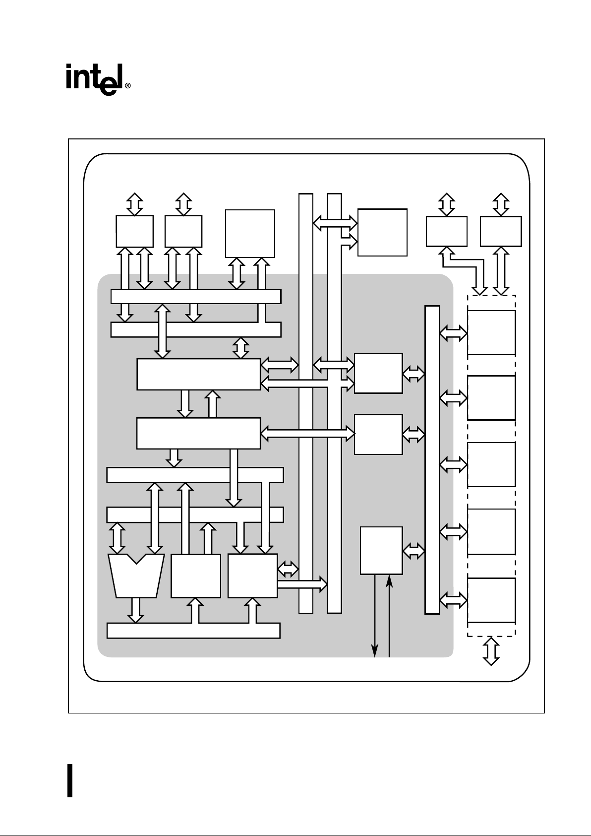
Figure 1. 8x930Ax Internal Block Diagram
A4340-01
SRC2 (8)
Code Address (24)
Code Bus (16)
RAM
ROM
Watchdog
Timer
Timer/
Counters
PCA
Serial I/O
Port 2
Drivers
P2.7:0
Port 0
Drivers
P0.7:0
Port 3
Drivers
P3.7:0
Port 1
Drivers
P1.7:0
Data Address (24)
Data Bus (8)
Memory Address (16)
System Bus and I/O Ports
I/O Ports and
Peripheral Signals
SRC1 (8)
IB Bus (8)
Peripheral
Interface
Interrupt
Handler
Clock
&
Reset
Bus Interface
Instruction Sequencer
DST (16)
ALU
Data
Memory
Interface
Memory Data (16)
Register
File
USB
†
USB Ports
Microcontroller Core
†
For details, see the USB module block diagram.
2 ADVANCE INFORMATION
8x930Ax UNIVERSAL SERIAL BUS (USB) MICROCONTROLLER
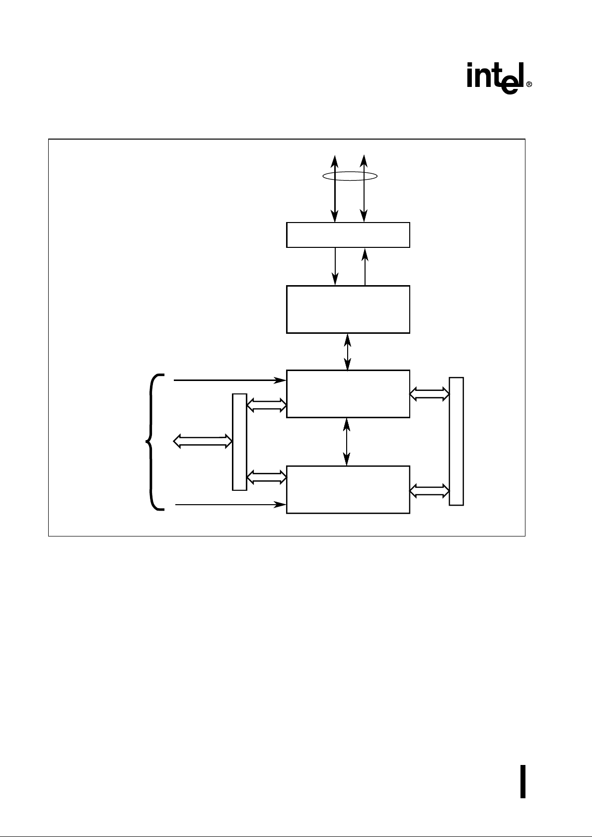
Figure 2. USB Module Block Diagram
D
P0
Transceiver
Control
Control
Control
Transmit/Receive Bus
FIFOs
D
M0
A4231-03
Data Bus
Serial Bus
Interface Engine
(SIE)
Function
Interface Unit
(FIU)
USB
Upstream
Port
To
CPU
ADVANCE INFORMATION 3
8x930Ax UNIVERSAL SERIAL BUS (USB) MICROCONTROLLER
1.0 NOMENCLATURE OVERVIEW
Figure 3. Product Nomenclature
Table 1. Description of Product Nomenclature
Parameter Options Description
Temperature and Burn-in no mark Commercial operating temperature range (0
o
C to 70oC) with
Intel standard burn-in.
Packaging Options N Plastic Leaded Chip Carrier (PLCC)
Program Memory Options 0 Without ROM
3 With ROM
Process and Voltage Information no mark CHMOS
Product Family 930 Advanced 8-bit microcontroller architecture with on-chip Uni-
versal Serial Bus (USB) function peripherals
Device Speed no mark 6 or 12 MHz crystal
Table 2. Proliferation Options
Product Name ROM Size RAM Size
80930AD 0 1 Kbyte
83930AD 8 Kbytes 1 Kbyte
83930AE 16 Kbytes 1 Kbyte
Program Memory Options
XXXXX XXXX8XXX
Packaging Options
Temperature and Burn-in Options
A2815-01
Process Information
Product Family
Device Speed
4 ADVANCE INFORMATION
8x930Ax UNIVERSAL SERIAL BUS (USB) MICROCONTROLLER
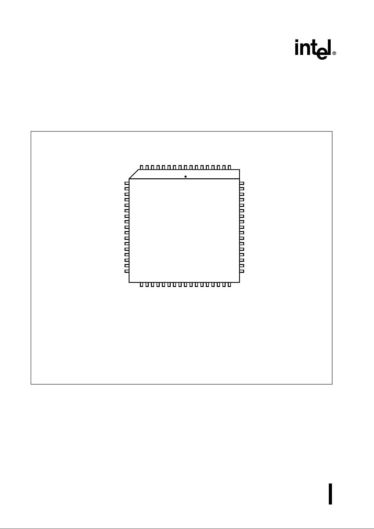
2.0 PINOUT
Figure 4. 8x930Ax 68-pin PLCC Package
Figure 4 illustrates the 8
x
930Ax PLCC package.
Table 3 lists the pin assignments by pin number,
and Table 4 lists the pin assignments by functional
categories. Table 5 describes the signals.
Reserved
Reserved
Reserved
Reserved
Reserved
D
P0
D
M0
ECAP
V
SSP
V
CCP
SOF#
Reserved
Reserved
Reserved
Reserved
Reserved
PLLSEL0
A8 / P2.0
A9 / P2.1
A10 / P2.2
A11 / P2.3
A12 / P2.4
A13 / P2.5
A14 / P2.6
A15 / P2.7
V
SSVCC
EA#
ALE
PSEN#
Reserved
Reserved
Reserved
Reserved
A4392-02
AD7 / P0.7
AD6 / P0.6
AD5 / P0.5
AD4 / P0.4
AD3 / P0.3
AD2 / P0.2
AD1 / P0.1
AD0 / P0.0
V
SSP
V
CCP
P3.0 / RXD
P3.1 / TXD
P3.2 / INT0#
P3.3 / INT1#
P3.4 / T0
P3.5 / T1
P3.6 / WR#
60
59
58
57
56
55
54
53
52
51
50
49
48
47
46
45
44
View of component as
mounted on PC board
10
11
12
13
14
15
16
17
18
19
20
21
22
23
24
25
26
P3.7 / RD# / A16
P1.0 / T2
P1.1 / T2EX
P1.2 / ECI
P1.3 / CEX0
P1.4 / CEX1
P1.5 / CEX2
P1.6 / CEX3 / WAIT#
P1.7 / CEX4 / A17 / WCLK
V
CC
V
SS
XTAL1
XTAL2
AV
CC
RST
PLLSEL1
PLLSEL2
27
28
29
30
31
32
33
34
35
36
37
38
39
40
41
42
43
987654321
68
67
66
65
64
63
62
61
Note: Reserved pins must be left unconnected.
ADVANCE INFORMATION 5
8x930Ax UNIVERSAL SERIAL BUS (USB) MICROCONTROLLER
Table 3. 68-pin PLCC Pin Assignment
Pin Name Pin Name Pin Name
1V
SS
24 P3.4/T0 47 Reserved
2 A15/P2.7 25 P3.5/T1 48 Reserved
3 A14/P2.6 26 P3.6/WR# 49 Reserved
4 A13/P2.5 27 P3.7/RD#/A16 50 SOF#
5 A12/P2.4 28 P1.0/T2 51 V
CCP
6 A11/P2.3 29 P1.1/T2EX 52 V
SSP
7 A10/P2.2 30 P1.2/ECI 53 ECAP
8 A9/P2.1 31 P1.3/CEX0 54 D
M0
9 A8/P2.0 32 P1.4/CEX1 55 D
P0
10 AD7/P0.7 33 P1.5/CEX2 56 Reserved
11 AD6/P0.6 34 P1.6/CEX3/WAIT# 57 Reserved
12 AD5/P0.5 35 P1.7/CEX4/A17/WCLK 58 Reserved
13 AD4/P0.4 36 V
CC
59 Reserved
14 AD3/P0.3 37 V
SS
60 Reserved
15 AD2/P0.2 38 XTAL1 61 Reserved
16 AD1/P0.1 39 XTAL2 62 Reserved
17 AD0/P0.0 40 AV
CC
63 Reserved
18 V
SSP
41 RST 64 Reserved
19 V
CCP
42 PLLSEL1 65 PSEN#
20 P3.0/RXD 43 PLLSEL2 66 ALE
21 P3.1/TXD 44 PLLSEL0 67 EA#
22 P3.2/INT0# 45 Reserved 68 V
CC
23 P3.3/INT1# 46 Reserved
6 ADVANCE INFORMATION
8x930Ax UNIVERSAL SERIAL BUS (USB) MICROCONTROLLER
Table 4. 68-pin PLCC Signal Assignments Arranged by Functional Category
Address & Data Input/Output USB
Name Pin Name Pin Name Pin
AD0/P0.0 17 P1.0/T2 28 PLLSEL0 44
AD1/P0.1 16 P1.1/T2EX 29 PLLSEL1 42
AD2/P0.2 15 P1.2/ECI 30 PLLSEL2 43
AD3/P0.3 14 P1.3/CEX0 31 SOF# 50
AD4/P0.4 13 P1.4/CEX1 32 ECAP 53
AD5/P0.5 12 P1.5/CEX2 33 D
M0
54
AD6/P0.6 11 P1.6/CEX3/WAIT# 34 D
P0
55
AD7/P0.7 10 P1.7/CEX4/A17/WCLK 35
A8/P2.0 9 P3.0/RXD 20 Processor Control
A9/P2.1 8 P3.1/TXD 21 Name Pin
A10/P2.2 7 P3.4/T0 24 P3.2/INT0# 22
A11/P2.3 6 P3.5/T1 25 P3.3/INT1# 23
A12/P2.4 5 EA# 67
A13/P2.5 4 Bus Control & Status RST 41
A14/P2.6 3 Name Pin XTAL1 38
A15/P2.7 2 P3.6/WR# 26 XTAL2 39
P3.7/RD#/A16 27 P3.7/RD#/A16 27
P1.7/CEX4/A17/WCLK 35 ALE 66
PSEN# 65
Power & Ground
Name Pin
V
CC
36, 68
V
CCP
19, 51
AV
CC
40
EA# 67
V
SS
1, 37
V
SSP
18, 52
ADVANCE INFORMATION 7
8x930Ax UNIVERSAL SERIAL BUS (USB) MICROCONTROLLER
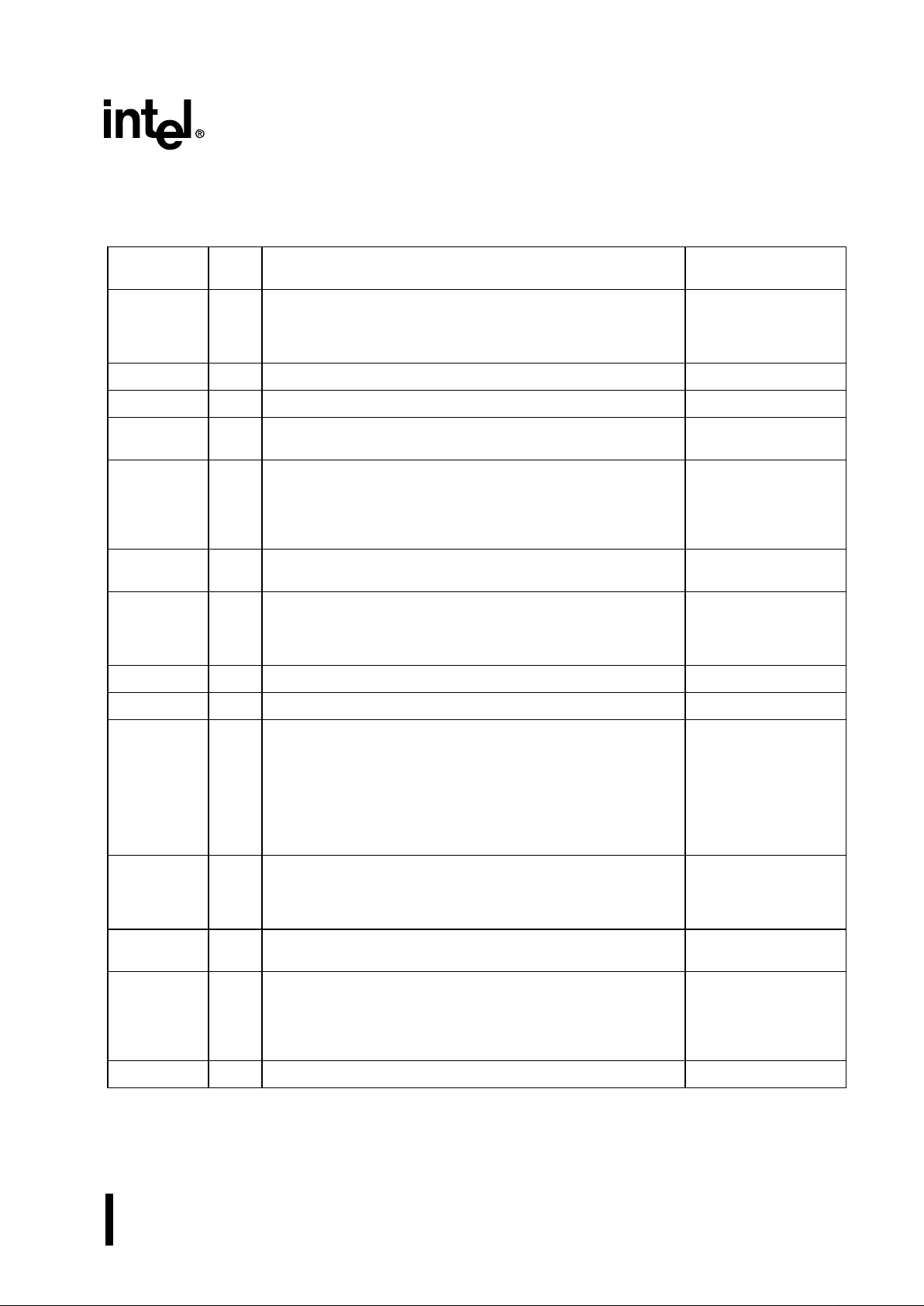
3.0 SIGNALS
Table 5. Signal Descriptions
Signal
Name
Type Description Alternate Function
A17 O 18th Address Bit (A17). Output to memory as 18th exter-
nal address bit (A17) in extended bus applications, depending on the values of bits RD0 and RD1 in configuration byte
UCONFIG0. See also RD#, PSEN#.
P1.7/CEX4/WCLK
A16 O Address Line 16. See RD#. RD#
A15:8
†
O Address Lines. Upper address lines for the external bus. P2.7:0
AD7:0
†
I/O Address/Data Lines. Multiplexed lower address lines and
data lines for external memory.
P0.7:0
ALE O Address Latch Enable (ALE). ALE signals the start of an
external bus cycle and indicates that valid address information is available on lines A15:8 and AD7:0. An external latch
can use ALE to demultiplex the address from the
address/data bus.
PROG#
AV
CC
PWR Analog VCC. A separate VCC input for the phase-locked loop
circuitry.
CEX2:0
CEX3
CEX4
I/O Programmable Counter Array (PCA) Input/Output Pins.
These are input signals for the PCA capture mode and output signals for the PCA compare mode and PCA PWM
mode.
P1.5:3
P1.6/WAIT#
P1.7/A17/WCLK
D
M0
I/O Data Minus. USB minus data line interface. —
D
P0
I/O Data Plus. USB plus data line interface. —
EA# I External Access. Directs program memory accesses to
on-chip or off-chip code memory. For EA# strapped to
ground, all program memory accesses are off-chip. For EA#
strapped to V
CC
, program accesses on-chip ROM if the
address is within the range of the on-chip ROM; otherwise,
the access is off-chip. The value of EA# is latched at reset.
For devices without on-chip ROM, EA# must be strapped to
ground.
ECAP I External Capacitor. Must be connected to a 1 µF capacitor
(or larger) to ensure proper operation of the differential line
driver. The other lead of the capacitor must be connected to
V
SS
.
ECI I PCA External Clock Input. External clock input to the 16-
bit PCA timer.
P1.2
INT1:0# I External Interrupts 0 and 1. These inputs set bits IE1:0 in
the TCON register. If bits IT1:0 in the TCON register are
set, bits IE1:0 are set by a falling edge on INT1#/INT0#. If
bits INT1:0 are clear, bits IE1:0 are set by a low level on
INT1:0#.
P3.3:2
P0.7:0 I/O Port 0. This is an 8-bit, open-drain, bidirectional I/O port. AD7:0
†
The descriptions of A15:8/P2.7:0 and AD7:0/P0.7:0 are for the nonpage-mode chip configuration. If the
chip is configured for page-mode operation, port 0 carries the lower address bits (A7:0), and port 2 carries the upper address bits (A15:8) and the data (D7:0).

8 ADVANCE INFORMATION
8x930Ax UNIVERSAL SERIAL BUS (USB) MICROCONTROLLER
P1.0
P1.1
P1.2
P1.5:3
P1.6
P1.7
I/O Port 1. This is an 8-bit, bidirectional I/O port with internal
pullups.
T2
T2EX
ECI
CEX2:0
CEX3/WAIT#
CEX4/A17/WCLK
P2.7:0 I/O Port 2. This is an 8-bit, bidirectional I/O port with internal
pullups.
A15:8
P3.0
P3.1
P3.3:2
P3.5:4
P3.6
P3.7
I/O Port 3. This is an 8-bit, bidirectional I/O port with internal
pullups.
RXD
TXD
INT1:0#
T1:0
WR#
RD#/A16
PLLSEL2:0 I Phase-locked Loop Select. Three-bit code selects USB
data rate (see Table 8 on page 12).
—
PSEN# O Program Store Enable. Read signal output. This output is
asserted for a memory address range that depends on bits
RD0 and RD1 in configuration byte UCONFIG0 (see RD#).
—
RD# O Read or 17th Address Bit (A16). Read signal output to
external data memory or 17th external address bit (A16),
depending on the values of bits RD0 and RD1 in configuration byte UCONFIG0 (See PSEN#).
P3.7/A16
RST I Reset. Reset input to the chip. Holding this pin high for 64
oscillator periods while the oscillator is running resets the
device. The port pins are driven to their reset conditions
when a voltage greater than V
IH1
is applied, whether or not
the oscillator is running. This pin has an internal pulldown
resistor which allows the device to be reset by connecting a
capacitor between this pin and V
CC
.
Asserting RST when the chip is in idle mode or powerdown
mode returns the chip to normal operation.
—
RXD I /O Receive Serial Data. RXD sends and receives data in
serial I/O mode 0 and receives data in serial I/O modes 1, 2,
and 3.
P3.0
SOF# O Start of Frame. Start of Frame pulse. Active low, asserted
for 8 states (see Table 8 on page 12 for state versus XTAL
clock) when Frame Timer is locked to USB frame timing
and SOF token or artificial SOF is detected.
—
T1:0 I Timer 1:0 External Clock Inputs. When timer 1:0 operates
as a counter, a falling edge on the T1:0 pin increments the
count.
P3.5:4
T2 I/O Timer 2 Clock Input/Output. For the timer 2 capture mode,
this signal is the external clock input. For the clock-out
mode, it is the timer 2 clock output.
P1.0
Table 5. Signal Descriptions (Continued)
Signal
Name
Type Description Alternate Function
†
The descriptions of A15:8/P2.7:0 and AD7:0/P0.7:0 are for the nonpage-mode chip configuration. If the
chip is configured for page-mode operation, port 0 carries the lower address bits (A7:0), and port 2 carries the upper address bits (A15:8) and the data (D7:0).

ADVANCE INFORMATION 9
8x930Ax UNIVERSAL SERIAL BUS (USB) MICROCONTROLLER
T2EX I Timer 2 External Input. In timer 2 capture mode, a falling
edge initiates a capture of the timer 2 registers. In autoreload mode, a falling edge causes the timer 2 registers to
be reloaded. In the up-down counter mode, this signal
determines the count direction: 1 = up, 0 = down.
P1.1
TXD O Transmit Serial Data. TXD outputs the shift clock in serial
I/O mode 0 and transmits serial data in serial I/O modes 1,
2, and 3.
P3.1
V
CC
PWR Supply Voltage. Connect this pin to the +5V supply volt-
age.
—
V
CCP
PWR Supply Voltage for I/O buffers. Connect this pin to the
+5V supply voltage.
—
V
SS
GND Circuit Ground. Connect this pin to ground. —
V
SSP
GND Circuit Ground for I/O b uf fers. Connect this pin to ground. —
WAIT# I Real-time Wait State Input. The real-time WAIT# input is
enabled by writing a logical ‘1’ to the WCON.0 (RTWE) bit
at S:A7H. During bus cycles, the external memory system
can signal ‘system ready’ to the microcontroller in real time
by controlling the WAIT# input signal on the port 1.6 input.
P1.6/CEX3
WCLK O Wait Clock Output. The real-time WCLK output is driven at
port 1.7 (WCLK) by writing a logical ‘1’ to the WCON.1
(RTWCE) bit at S:A7H. When enabled, the WCLK output
produces a square wave signal with a period of T
CLK
.
P1.7/CEX4/A17
WR# O Write. Write signal output to external memory. P3.6
XTAL1 I Input to the On-chip, Inverting, Oscillator Ampli fi er. To
use the internal oscillator, a crystal/resonator circuit is connected to this pin. If an external oscillator is used, its output
is connected to this pin. XTAL1 is the clock source for internal timing.
—
XTAL2 O Output of the On-chip, Inverting, Oscillator Amplifier. To
use the internal oscillator, a crystal/resonator circuit is connected to this pin. If an external oscillator is used, leave
XTAL2 unconnected.
—
Table 5. Signal Descriptions (Continued)
Signal
Name
Type Description Alternate Function
†
The descriptions of A15:8/P2.7:0 and AD7:0/P0.7:0 are for the nonpage-mode chip configuration. If the
chip is configured for page-mode operation, port 0 carries the lower address bits (A7:0), and port 2 carries the upper address bits (A15:8) and the data (D7:0).

10 ADVANCE INFORMATION
8x930Ax UNIVERSAL SERIAL BUS (USB) MICROCONTROLLER
†
RD1:0 are bits 3:2 of configuration byte UCONFIG0. Refer to figure 4-3 on page 4-5 in the
8x930Ax Uni-
versal Serial Bus Microcontroller User’s Manual
.
4.0 ADDRESS MAP
Table 6. Memory Signal Selections (RD1:0)
RD1:0
†
A17/P1.7
/CEX4/WCLK
A16/P3.7/RD# PSEN# WR# Features
0 0 A17 A16 Asserted for
all addresses
Asserted for writes to
all memory locations
256-Kbyte external
memory
0 1 P1.7/CEX4/WCLK A16 Asserted for
all addresses
Asserted for writes to
all memory locations
128-Kbyte external
memory
1 0 P1.7/CEX4/WCLK P3.7 only Asserted for
all addresses
Asserted for writes to
all memory locations
64-Kbyte external
memory
One additional port
pin
1 1 P1.7/CEX4/WCLK RD# Asserted
for addresses
≤ 7F:FFFFH
Asserted for
addresses
≥ 80:0000H
Asserted for all compatible MCS 51 memory locations
Compatible with
MCS 51 microcontrollers
Table 7. 8
x
930Ax Address Map
Internal
Address
Description Notes
FF:FFFFH
FF:0000H
External Memory: The last eight bytes of the external address range FF:XFF8H–
FF:XFFFH contain configuration byte information.
1, 2, 3
FE:FFFFH
FE:0000H
External Memory 2
FD:FFFFH
02:0000H
Reserved Addresses 4
01:FFFFH
01:0000H
External Memory 2
00:FFFFH
00:0420H
External Memory 5
00:041FH
00:0080H
On-chip RAM 5
00:007FH
00:0020H
On-chip RAM 6
00:001FH
00:0000H
Storage for R0–R7 of Register File 7, 8
NOTES:
1. E ighteen address lines are bonded out (A15:0, A16:0, or A17:0 selected during chip configuration).
2. Data in this area is accessible by indirect addressing only.
3. Eight addresses at the top of all external memory maps are reserved for current and future device
configuration byte information.
4. This reser ved area returns unspecified values and writes no data.
5. Data is accessible by direct and indirect addressing.
6. Data is accessible by direct, indirect, and bit addressing.
7. The spec ial function registers (SFRs) and the register file have separate internal address spaces.
8. Data is accessible by direct, indirect, and register addressing.

ADVANCE INFORMATION 11
8x930Ax UNIVERSAL SERIAL BUS (USB) MICROCONTROLLER
5.0 ELECTRICAL CHARACTERISTICS
ABSOLUTE MAXIMUM RATINGS
Ambient Temperature Under Bias.................... -40°C to +85°C
Storage Temperature ................................... -65°C to +150°C
Voltage on Any Pins to V
SS
............................. -0.5 V to +6.5 V
I
OL
per I/O Pin................................................................. 15 mA
Power Dissipation .......................................................... 1.5 W
OPERATING CONDITIONS
†
TA (Ambient Temperature Under Bias):
Commercial........................................................ -0°C to +70°C
V
CC/VCCP
(Digital Supply Voltage) .................. 4.00 V to 5.25 V
V
SS
/ V
SSP
............................................................................ 0 V
AV
CC
(Analog Supply Voltage) ...................... 4.00 V to 5.25 V
F
OSC
....................... ..... ..... ...... ....................... 6 MHz or 12 MHz
NOTE: Maximum power dissipation is based on
package heat-transfer limitations, not device
power consumption.
NOTICE: This document contains information on
products in the sampling and initial production
phases of development. The specifications are
subject to change without notice. Verify with your
local Intel sales office that you have the latest
datasheet before finalizing a design.
†
WARNING: Stressing the device beyond the
“Absolute Maximum Ratings” may cause permanent damage. These are stress ratings only. Operation beyond the “Operating Conditions” is not
recommended and extended exposure beyond the
“Operating Conditions” may affect device
reliability.

12 ADVANCE INFORMATION
8x930Ax UNIVERSAL SERIAL BUS (USB) MICROCONTROLLER
5.1 Operating Frequencies
Figure 5. Clock Circuit
Table 8. Frequency Selection and Operating Frequency
PLLSEL2
Pin 43
PLLSEL1
Pin 42
PLLSEL0
Pin 44
USB Rate
(Low
Speed
or Full
Speed)
8
x
930A
x
Internal
Frequency
for CPU
and
Peripherals
(F
CLK
)
(5)
XTAL1
External
Frequency
(F
OSC
)
Number of
XTAL1
Clocks
(T
OSC
)
in One
StateTime
(4)
Comments
0 0 1 1.5 Mbps
(LS)
3 MHz 6 MHz 2 T
OSC
/state PLL Off
1 0 0 1.5 Mbps
(LS)
6 MHz (3) 12 MHz 2 T
OSC
/state PLL Off
1 1 0 12 Mbps
(FS)
12 MHz (3) 12 MHz 1 T
OSC
/state PLL On
NOTES:
1. Other PLLSEL
x
combinations are not valid.
2. The sampling rate is 4X the USB rate.
3. The 8
x
930Ax CPU and peripherals frequency is 3 MHz (low clock mode) until firmware disables the
low clock mode.
4. The number of XTAL clocks in one state depends on the PLLSELx selections. When the CPU is operating at low clock mode (3 MHz), there are four T
OSC
per state for the PLLSEL2:1:0 = 100 and 110.
5. The AC timing specification (Table 11) defines the following symbol: CPU frequency = F
CLK
= 1/T
CLK
.
Clock
Generator
A5135-01
XTAL1
XTAL2
F
OSC
(6 or 12 MHz)
PCON.0
(Idle Mode)
IDL
PCON.1
(Powerdown)
0
1
PD
÷ 2
102
PLLSEL
F
CLK
CPU
On-chip
Peripherals
Internal Clock
PCON.5
(Low-clock Mode)
LC
0
1
3 MHz

ADVANCE INFORMATION 13
8x930Ax UNIVERSAL SERIAL BUS (USB) MICROCONTROLLER
5.2 DC Characteristics
Table 9. DC Characteristics at Operating Conditions
Symbol Parameter Min Typical (1) Max Units Test Conditions
V
IL
Input Low Voltage
(Except EA#)
-0.5 0.2 V
CC
– 0.1
V
V
IL1
Input Low Voltage
(EA#)
00.2 V
CC
– 0.3
V
V
IH
Input High Voltage
(Except XTAL1, RST)
0.2 V
CC
+ 0.9 V
CC
+ 0.5
V
V
IH1
Input High Voltage
(XTAL1, RST)
0.7 V
CC
V
CC
+ 0.5
V
V
OL
Output Low Voltage
(Port 1, 2, 3)
0.3
0.45
1.0
V
I
OL
= 100 µA (2, 3)
I
OL
= 1.6 mA
I
OL
= 3.5 mA
V
OL1
Output Low Voltage
(Port 0, ALE, PSEN#,
SOF#)
0.3
0.45
1.0
V
I
OL
= 200 µA (2, 3)
I
OL
= 3.2 mA
I
OL
= 7.0 mA
V
OH
Output High Voltage
(Port 1, 2, 3,ALE,
PSEN#, SOF#)
V
CC
– 0.3
V
CC
– 0.7
V
CC
– 1.5
V
I
OH
= -10 µA (4)
I
OH
= -30 µA
I
OH
= -60 µA
V
OH1
Output High Voltage
(Port 0 in External
Address)
V
CC
– 0.3
V
CC
– 0.7
V
CC
– 1.5
V
I
OH
= -200 µA (4)
I
OH
= -3.2 mA
I
OH
= -7.0 mA
I
IL
Logical 0 Input
Current (Port 1,2,3)
–150
µA
VIN = 0.45 V
I
LI
Input Leakage Current
(Port 0)
±10
µA
0.45 < V
IN
< V
CC
NOTE:
1. Typical values are obtained using V
CC
= 5.0V, TA = 25°C and are not guaranteed.
2. Under steady state (non-transient) conditions, I
OL
must be externally limited as follows:
Maximum I
OH
per port pin:10 mA
Maximum I
OL
per 8-bit port:
Port 0: 26 mA Ports 1-3: 15 mA
Maximum Total I
OL
for all output pins: 71 mA
If I
OL
exceeds the test conditions, VOL may exceed the related specification. Pins are not guaranteed
to sink current greater than the listed test conditions.
3. Capacitive loading on Ports 0 and 2 may cause spurious noise pulses above 0.4 V on the low-level
outputs of ALE and Ports 1, 2 and 3. The noise is due to external bus capacitance discharging into the
Port 0 and Port 2 pins when these pins change from 1 to 0. In applications where capacitive loading
exceeds 100pF, the noise pulses on these signals may exceed 0.8 V. It may be desirable to qualify
ALE or other signals with a Schmitt Trigger or CMOS-level input logic.
4. Capacitive loading on Ports 0 and 2 cause the V
OH
on ALE and PSEN to drop below the VCC specifica-
tion when the address lines are stabilizing.
5. The abbreviations “LS” and “FS” indicate “Low Speed” and “Full Speed,” respectively.

14 ADVANCE INFORMATION
8x930Ax UNIVERSAL SERIAL BUS (USB) MICROCONTROLLER
I
TL
Logical 1-to-0
Transition Current
(Port 1, 2,3)
-650
µA
V
IN
= 2.0 V
R
RST
RST Pulldown
Resistor
40 225
KΩ
C
IO
10
pF
F
OSC
= 12 MHz
T
A
= 25°C
I
PD
Powerdown Current
— Normal powerdown
— USB suspend
25
145
50
175
µA
I
DL
(5) Idle Mode ICC 40
mA
PLLSEL = 110
3MHz – FS
(in low clock mode)
100 PLLSEL = 110
12MHz – FS
(not in low clock
mode)
30 PLLSEL = 001
3MHz – LS
55 PLLSEL = 100
6 MHz – LS
Table 9. DC Characteristics at Operating Conditions (Continued)
Symbol Parameter Min Typical (1) Max Units Test Conditions
NOTE:
1. Typical values are obtained using V
CC
= 5.0V, TA = 25°C and are not guaranteed.
2. Under steady sta te (non-transient) conditions, I
OL
must be externally limited as follows:
Maximum I
OH
per port pin:10 mA
Maximum I
OL
per 8-bit port:
Port 0: 26 mA Ports 1-3: 15 mA
Maximum Total I
OL
for all output pins: 71 mA
If I
OL
exceeds the test conditions, VOL may exceed the related specification. Pins are not guaranteed
to sink current greater than the listed test conditions.
3. Capacitive loading on Ports 0 and 2 may cause spurious noise pulses above 0.4 V on the low-level
outputs of ALE and Ports 1, 2 and 3. The noise is due to external bus capacitance discharging into the
Port 0 and Port 2 pins when these pins change from 1 to 0. In applications where capacitive loading
exceeds 100pF, the noise pulses on these signals may exceed 0.8 V. It may be desirable to qualify
ALE or other signals with a Schmitt Trigger or CMOS-level input logic.
4. Capacitive loading on Ports 0 and 2 cause the V
OH
on ALE and PSEN to drop below the VCC specifica-
tion when the address lines are stabilizing.
5. The abbreviations “LS” and “FS” indicate “Low Speed” and “Full Speed,” respectively.

ADVANCE INFORMATION 15
8x930Ax UNIVERSAL SERIAL BUS (USB) MICROCONTROLLER
5.3 Definition of AC Symbols
ICC (5) Active ICC 60
mA
PLLSEL = 110
3 MHz – FS
(in low clock mode)
150 PLLSEL = 110
12 MHz – FS
(not in low clock
mode)
45 PLLSEL = 001
3 MHz – LS
75 PLLSEL = 100
6 MHz – LS
Table 10. AC Timing Symbol Definitions
Signals Conditions
A Address H High
D Data In L Low
L ALE V Valid
Q Data Out X Hold
R RD#/PSEN# Z Floating
WWR#
Table 9. DC Characteristics at Operating Conditions (Continued)
Symbol Parameter Min Typical (1) Max Units Test Conditions
NOTE:
1. Typical values are obtained using V
CC
= 5.0V, TA = 25°C and are not guaranteed.
2. Under steady state (non-transient) conditions, I
OL
must be externally limited as follows:
Maximum I
OH
per port pin:10 mA
Maximum I
OL
per 8-bit port:
Port 0: 26 mA Ports 1-3: 15 mA
Maximum Total I
OL
for all output pins: 71 mA
If I
OL
exceeds the test conditions, VOL may exceed the related specification. Pins are not guaranteed
to sink current greater than the listed test conditions.
3. Capacitive loading on Ports 0 and 2 may cause spurious noise pulses above 0.4 V on the low-level
outputs of ALE and Ports 1, 2 and 3. The noise is due to external bus capacitance discharging into the
Port 0 and Port 2 pins when these pins change from 1 to 0. In applications where capacitive loading
exceeds 100pF, the noise pulses on these signals may exceed 0.8 V. It may be desirable to qualify
ALE or other signals with a Schmitt Trigger or CMOS-level input logic.
4. Capacitive loading on Ports 0 and 2 cause the V
OH
on ALE and PSEN to drop below the VCC specifica-
tion when the address lines are stabilizing.
5. The abbreviations “LS” and “FS” indicate “Low Speed” and “Full Speed,” respectively.

16 ADVANCE INFORMATION
8x930Ax UNIVERSAL SERIAL BUS (USB) MICROCONTROLLER
5.4 AC Characteristics
Test Conditions: Capacitive load on all pins = 50 pF, Rise and Fall times = 10 ns, F
OSC
= 6 MHz or 12 MHz
5.4.1 SYSTEM BUS AC CHARACTERISTICS
Table 11. AC Characteristics at Operating Conditions
Symbol Parameter
CPU Frequency
@ 12 MHz
(M, N = 0)
CPU Frequency (F
CLK
) Variable
Units
Min Max
T
CLK
1/(CPU Frequency) 83.33
(Typical)
ns
(1, 2)
T
LHLL
ALE Pulse Width 34.66 (0.5+M)T
CLK
– 7 ns (3)
T
AVLL
Address Valid to ALE Low 26.66 (0.5+M)T
CLK
–
17
ns (3)
T
LLAX
Address Hold after ALE Low 4 4 ns (4)
T
RLRH
(5) RD# or PSEN# Pulse Width 73.33 (1+N)T
CLK
– 10 ns (6)
T
WLWH
WR# Pulse Width 71.33 (1+N)T
CLK
– 12 ns (6)
T
LLRL
(5) AL E Low to RD# or PSEN# Low 8 8 ns
T
LHAX
ALE High to Address Hold 40.33 (1+M)T
CLK
– 43 ns (3)
T
RLDV
(5) RD# or PSEN# Low to Valid
Data/Instruction In
50.33 (1+N)T
CLK
– 33 ns (6)
T
RHDX
(5) Data/Instruct. Hold After RD# or
PSEN# High
00 ns
T
RLAZ
(5) RD# or PSEN# Low to Address
Float
00ns
T
RHDZ1
(5) Instruct. Float After PSEN# High 10 10 ns
T
RHDZ2
(5) Data Float After RD# or PSEN#
High
83.33 T
CLK
ns
T
RHLH1
(5) PSEN# High to ALE High
(Instruction)
10 10 ns
T
RHLH2
(5) RD# or PSE N# High to ALE
High (Data)
83.33 T
CLK
ns
T
WHLH
WR# High to ALE High 88.33 T
CLK
+ 5 ns
T
AVDV1
Address (P0) Valid to Valid
Data/Instruction In
106.66 (2+M+N)T
CLK
–63ns
(3, 6)
NOTES:
1. Refer to Table 8 on page 12 for CPU frequencies vs. XTAL1 frequencies.
2. XTAL1 fr equency is ± 0.25% for full speed and ± 1.5% for low speed.
3. M= 0,1 is the extended ALE state.
4. At 50° C, T
LLAX
= 8 ns
5. Specifications for PSEN# are identical to those for RD#.
6. N= 0,1,2,3 is the RD#/PSEN#/WR# wait state.

ADVANCE INFORMATION 17
8x930Ax UNIVERSAL SERIAL BUS (USB) MICROCONTROLLER
T
AVDV2
Address (P2) Valid to Valid
Data/Instruction In
118.66 (2+M+N)T
CLK
– 48
ns
(3, 6)
T
AVDV3
Address (P2) Valid to Valid
Instruction In
23.33 (1+N)T
CLK
– 60 ns (6)
T
AVRL
(5) Address Valid to RD# or PSEN#
Low
40.33 (1+M)T
CLK
– 46 ns (3)
T
AVWL1
Address (P0) Valid to WR# Low 40.33 (1+M )T
CLK
– 46 ns (3)
T
AVWL2
Address (P2) Valid to WR# Low 66.33 (1+M )T
CLK
– 17 ns (3)
T
WHQX
Data Hold after WR# High 28.66 0.5 T
CLK
– 13 ns
T
QVWH
Data Valid to WR# High 68.33 (1+N)T
CLK
–15 ns (6)
T
WHAX
WR# High to Address Hold 70.33 T
CLK
– 13 ns
Table 11. AC Characteristics at Operating Conditions (Continued)
Symbol Parameter
CPU Frequency
@ 12 MHz
(M, N = 0)
CPU Frequency (F
CLK
) Variable
Units
Min Max
NOTES:
1. Refer to Table 8 on page 12 for CPU frequencies vs. XTAL1 frequencies.
2. XTAL1 fr equency is ± 0.25% for full speed and ± 1.5% for low speed.
3. M= 0,1 is the extended ALE state.
4. At 50° C, T
LLAX
= 8 ns
5. Specifications for PSEN# are identical to those for RD#.
6. N= 0,1,2,3 is the RD#/PSEN#/WR# wait state.

18 ADVANCE INFORMATION
8x930Ax UNIVERSAL SERIAL BUS (USB) MICROCONTROLLER
5.4.2 SYSTEM BUS TIMING DIAGRAMS, NONPAGE MODE
Figure 6. 8
x
930Ax Code Fetch, Nonpage Mode
ALE
RD#/PSEN#
P0
A17/A16/P2
A5011-01
State 1 State 1
(next cycle)
State 2
T
LHLL
T
LLRL
T
RLRH
T
RLAZ
T
LLAX
T
AVLL
T
AVDV1
T
AVDV2
T
LHAX
Instruction In
A7:0
A17/A16/A15:8
T
RHDX
T
RHDZ1
T
RHLH1
T
AVRL
T
RLDV

ADVANCE INFORMATION 19
8x930Ax UNIVERSAL SERIAL BUS (USB) MICROCONTROLLER
Figure 7. 8x930Ax Data Read, Nonpage Mode
Figure 8. 8
x
930Ax Data Write, Nonpage Mode
ALE
RD#/PSEN#
P0
A17/A16/P2
A5025-02
State 1 State 3State 2
T
LHLL
T
LLRL
T
RLRH
T
RLAZ
T
LLAX
T
RLDV
T
AVDV1
T
AVDV2
T
LHAX
D7:0
A7:0
A17/A16/A15:8
T
RHDX
T
RHDZ2
T
RHLH2
T
AVRL
T
AVLL
T
QVWH
ALE
WR#
P0
A17/A16/P2
A5026-02
State 1 State 3State 2
T
LHLL
T
WLWH
T
LLAX
T
LHAX
D7:0
A7:0
A17/A16/A15:8
T
WHLH
T
AVWL2
T
AVLL
T
AVWL1
T
WHAX
T
WHQX

20 ADVANCE INFORMATION
8x930Ax UNIVERSAL SERIAL BUS (USB) MICROCONTROLLER
5.4.3 SYSTEM BUS TIMING DIAGRAMS, PAGE MODE
Figure 9. 8
x
930Ax Code Fetch, Page Mode
ALE
RD#/PSEN#
P2
A17/A16/P0
A5028-02
State 1
State 2
T
LHLL
T
LLRL
T
RLRH
T
RLAZ
T
LLAX
T
AVLL
T
AVDV1
T
AVDV2
T
LHAX
Instruction 1 In
A15:8
A17/A16/A7:0
T
RHDZ1
T
RHLH1
T
AVRL
T
RLDV
T
RHDX
Instruction 2 In
T
AVDV3
Cycle 2, Page Hit
State 1
Cycle 1, Page Miss
†
During a sequence of page hits, PSEN# remains low until the end of the last page hit cycle.
†

ADVANCE INFORMATION 21
8x930Ax UNIVERSAL SERIAL BUS (USB) MICROCONTROLLER
Figure 10. 8x930Ax Data Read, Page Mode
Figure 11. 8
x
930Ax Data write, Page Mode
ALE
RD#/PSEN#
P2
A17/A16/P0
A5029-02
State 1 State 3State 2
T
LHLL
T
LLRL
T
RLRH
T
RLAZ
T
LLAX
T
RLDV
T
AVDV1
T
AVDV2
T
LHAX
D7:0
A15:8
A17/A16/A7:0
T
RHDX
T
RHDZ2
T
AVRL
T
AVLL
T
RHLH2
T
QVWH
ALE
WR#
P2
A17/A16/P0
A5030-02
State 1 State 3State 2
T
LHLL
T
WLWH
T
LLAX
T
LHAX
D7:0
A15:8
A17/A16/A7:0
T
WHLH
T
AVWL2
T
AVLL
T
AVWL1
T
WHAX
T
WHQX

22 ADVANCE INFORMATION
8x930Ax UNIVERSAL SERIAL BUS (USB) MICROCONTROLLER
5.4.4 DEFINITION OF REAL-TIME WAIT SYMBOLS
5.4.5 REAL-TIME WAIT FUNCTION AC CHARACTERISTICS
Table 12. Real-time Wait Timing Symbol Definitions
Signals Conditions
A Address L Low
D Data X Hold
C WCLK V Setup
YWAIT#
WWR#
R RD#/PSEN#
Table 13. Real-time Wait AC Timing Specifications
Symbol Parameter
F
CLK
Variable
(1) (2)
Units
Min Typ Max
T
CLYV
Wait Clock Low to Wait Setup 0 0.5 T
CLK
– 13 ns
T
CLYX
Wait Hold after Wait Clock Low (W)T
CLK
+ 5 (0.5+W)T
CLK
– 13 ns
T
RLYV
PSEN# or RD# Low to Wait Setup 0 0.5 T
CLK
– 13 ns
T
RLYX
Wait Hold after PSEN# or RD# Low (W)T
CLK
+ 5 (0.5+W)T
CLK
– 13 ns
T
WLYV
WR# Low to Wait Setup 0 0.5 T
CLK
– 13 ns
T
WLYX
Wait Hold after WR# Low (W)T
CLK
+ 5 (0.5+W)T
CLK
– 13 ns
NOTES:
1. W = 0, 1, 2, ... is the number of real-time wait states.
2. Real-time Wait function has a critical timing for instruction read. It is not advisable to use this feature
for instruction read during page mode.

ADVANCE INFORMATION 23
8x930Ax UNIVERSAL SERIAL BUS (USB) MICROCONTROLLER
5.4.6 REAL-TIME WAIT FUNCTION TIMING DIAGRAMS
Figure 12. External Code Fetch/Data Read (Nonpage Mode, Real-time Wait State)
A7:0
WCLK
ALE
RD#/PSEN#
WAIT#
P0
P2
A15:8
A5000-02
State 1 State 2 State 3 State 1 (next cycle)
T
CLYX
min
T
CLYV
A7:0D7:0 stretched
A15:8 stretched
RD#/PSEN# stretched
T
CLYX
max
T
RLYV
T
RLYX
max
T
RLYX
min

24 ADVANCE INFORMATION
8x930Ax UNIVERSAL SERIAL BUS (USB) MICROCONTROLLER
Figure 13. External Data Write (Nonpage Mode, Real-time Wait State)
A7:0
WCLK
ALE
WR#
T
WLYV
WAIT#
P0
P2
A5002-02
State 1 State 2 State 3 State 4
T
CLYX
min
T
CLYV
D7:0
stretched
A15:8 stretched
WR# stretched
T
WLYX
max
T
WLYX
min
T
CLYX
max

ADVANCE INFORMATION 25
8x930Ax UNIVERSAL SERIAL BUS (USB) MICROCONTROLLER
Figure 14. External Data Read (Page Mode, Real-time Wait State)
A15:8
WCLK
ALE
RD#/PSEN#
WAIT#
P2
P0
A7:0
A5001-02
State 1 State 2 State 3 State 1 (next cycle)
T
CLYX
min
T
CLYV
A15:8D7:0 stretched
A7:0 stretched
RD#/PSEN# stretched
T
CLYX
max
T
RLYV
T
RLYX
max
T
RLYX
min

26 ADVANCE INFORMATION
8x930Ax UNIVERSAL SERIAL BUS (USB) MICROCONTROLLER
Figure 15. External Data Write (Page Mode, Real-time Wait State)
A15:8
WCLK
ALE
WR#
T
WLYV
WAIT#
P2
P0
A5003-02
State 1 State 2 State 3 State 4
T
CLYX
min
T
CLYV
D7:0 stretched
A7:0 stretched
WR# stretched
T
WLYX
max
T
WLYX
min
T
CLYX
max

ADVANCE INFORMATION 27
8x930Ax UNIVERSAL SERIAL BUS (USB) MICROCONTROLLER
5.5 AC Characteristics — Serial Port, Synchronous Mode 0
Figure 16. Serial Port Waveform — Synchronous Mode 0
Table 14. Serial Port Timing — Synchronous Mode 0
Symbol Parameter Min Max Units
T
XLXL
Serial Port Clock Cycle Time 6 T
OSC
ns
T
QVSH
Output Data Setup to Clock Rising Edge 5 T
OSC
– 133 ns
T
SHQX
Output Data hold after Clock Rising Edge T
OSC
– 50 ns
T
XHDX
Input Data Hold after Clock Rising Edge 0 ns
T
XHDV
Clock Rising Edge to Input Data Valid 5 T
OSC
– 133 ns
Valid
Valid
Valid Valid
Valid Valid
Valid
Valid
RXD
(In)
RXD
(Out)
TXD
01 2
3
4
5
6
7
T
QVXH
T
XLXL
T
XHDX
T
XHQX
T
XHDV
A2592-02
Set TI
†
Set RI
†
†
TI and RI are set during S1P1 of the peripheral cycle following the shift of the eighth bit.

28 ADVANCE INFORMATION
8x930Ax UNIVERSAL SERIAL BUS (USB) MICROCONTROLLER
5.6 External Clock Drive
Figure 17. External Clock Drive Waveforms
Table 15. External Clock Drive
Symbol Parameter Min Max Units
1/T
OSC
Oscillator Frequency (F
OSC
)612MHz
T
CHCX
High Time 0.35 T
OSC
0.65 T
OSC
ns
T
CLCX
Low Time 0.35 T
OSC
0.65 T
OSC
ns
T
CLCH
Rise Time 10 ns
T
CHCL
Fall Tim e 10 ns
0.7 VCC
A4119-01
0.45 V
VCC – 0.5
0.2 V
CC
– 0.1
T
CHCL
T
CLCX
T
CLCL
T
CLCH
T
CHCX

ADVANCE INFORMATION 29
8x930Ax UNIVERSAL SERIAL BUS (USB) MICROCONTROLLER
5.7 Testing Waveforms
Figure 18. AC Testing Input, Output Waveforms
Figure 19. Float Waveforms
AC inputs during testing are driven at V
CC
– 0.5V for a logic 1
and 0.45 V for a logic 0. Timing measurements are made at
0.45 V
Inputs
Outputs
A4118-01
V
IH
MIN
V
OL
MAX
V
CC
– 0.5
0.2 V
CC
+ 0.9
0.2 V
CC
– 0.1
a min of V
IH
for a logic 1 and V
OL
for a logic 0.
V
LOAD
+ 0.1 V
V
LOAD
– 0.1 V
Timing Reference
Points
V
LOAD
V
OH
– 0.1 V
V
OL
+ 0.1 V
For timing purposes, a port pin is no longer floating when a
100 mV change from load voltage occurs and begins to float
when a 100 mV change from the loading V
OH/VOL
level occurs
with I
OL
/
I
OH
= ± 20 mA.
A4117-01

30 ADVANCE INFORMATION
8x930Ax UNIVERSAL SERIAL BUS (USB) MICROCONTROLLER
6.0 THERMAL CHARACTERISTICS
This microcontroller operates over the commercial
temperature range from 0
o
C to 70oC. All thermal
impedance data (Table 16) is approximate for static
air conditions at 1 watt of power dissipation. Values
change depending on operating conditions and
application requirements. The Intel
Packaging
Handbook
(order number 240800) describes Intel’s
thermal impedance test methodology. The
Components Quality and Reliability Handbook
(order number 210997) provides quality and
reliability information.
7.0 PRODUCT REFERENCE
This section lists design considerations for the
8x930Ax Universal Serial Bus microcontroller.
7.1 External Bus Timing and
Peripheral Timing Affected by
PLLSEL2:0 Selection
PLLSEL2 (pin43), PLLSEL1 (pin 42), and PLLSEL0
(pin 44) determine the 8
x
930Ax internal CPU
operating frequency. The selected CPU operating
frequency also influences all the peripherals. If the
PLLSEL2:0 pins of the 8
x
930Ax are set to 110, then
the internal clock frequency is 12MHz, and one
state time equals one clock time (please refer to
Table 8 on page 12). Therefore, all internal and
external instruction times for the timer, serial port,
PCA, are two times faster than with other
PLLSEL2:0 selections. Refer to the
8x930Ax,
8x930Hx Universal Serial Bus Microcontroller
User’s Manual
for the new peripheral timing
formulas.
7.2 Low Clock Mode Frequency
In low clock mode, the CPU and peripherals run at 3
MHz. All external bus accesses are affected,
including instruction fetch, data read/write, and
peripheral timing. Please refer to Table 8 on page
12 for the relationship of 3 MHz CPU and peripheral
timing (T
CLK
) to state times. One peripheral cycle is
6 state times.
7.3 Setting FFRC Bit Clears Only the
Oldest Packet in the FIFO
If the receive FIFO is set as a dual packet mode, it
can receive two packets. Setting FFRC to indicate
FIFO Read Complete will not flush the entire FIFO,
only the oldest packet will be flushed. The read
marker will be advanced to the location of the read
pointer.
7.4 Series Resistor Requirement for
Impedance Matching
Per the USB 1.0 specification (page 111, section
7.1.1.1), the impedance of the differential driver
must be between 29 and 44 Ohms. To match the
cable impedance, a series resistor of 27 to 33 Ohms
should be connected to each USB line; i.e., on D
P0
(pin 55) and on DM0 (pin 54). If the USB line is
improperly terminated or not matched, signal fidelity
will suffer. This can be seen on the scope as
excessive overshoot and undershoot. This will
potentially introduce bit errors.
7.5 Pullup Requirement for Full
Speed Device and Low Speed
Device
The pullup is a USB requirement to allow the host to
identify which devices are low speed and which are
full speed in order to communicate at the appropriate data rate. For Full Speed devices (12 Mbps)
use a 1.5K pullup resistor (to 3.0 V – 3.6 V) on the
D
P0
line. For Low Speed devices (1.5Mbps), use a
1.5K pullup resistor (to 3.0 V – 3.6 V) on the D
M0
line.
7.6 Powerdown Mode Cannot Be
Invoked Before USB Suspend
If the 8x930Ax is put into powerdown mode prior to
receiving a USB Suspend signal from the host, a
USB Resume will not properly wake up the
8
x
930Ax from powerdown mode.
Table 16. Thermal Characteristics
Package Type θ
JA
θ
JC
68-pin PLCC N/A N/A

ADVANCE INFORMATION 31
8x930Ax UNIVERSAL SERIAL BUS (USB) MICROCONTROLLER
8.0 SPECIFICATION SUPPLEMENT
FOR 8
X
930AX3 AND 8X930AX4
All descriptions above apply to the 8x930Ax and
8
x
930Ax2 microcontrollers. The following specifica-
tions apply to recent steppings of the 8
x
930A
x
(8x930Ax3 and 8x930Ax4). This information is in
addition to (or in place of) the specifications
described above.
8.1 Six Endpoint Pairs Functionality
In the default state, the SIXEPPEN bit of
8
x
930Ax3’s and 8x930Ax4’s EPCONFIG SFR is
cleared and the 6 endpoint pair feature is disabled.
In this state, the endpoint pairs of the 8
x
930Ax3 and
8
x
930Ax4 are similar to those of the 8x930Ax and
8
x
930Ax2 devices.
To enable the 6 endpoint pair feature, set
EPCONFIG’s SIXEPPEN bit. The 8
x
930Ax3 and
8
x
930Ax4 will then have the endpoint pairs shown
in Table 17.
When the 6 endpoint pair feature is enabled, two
additional SFRs — the Function Interrupt Enable
Register 1 (FIE1) and the Function Interrupt Flag
Register 1 (FIFLG1) — are enabled to manage
interrupts for the additional endpoint pairs.
See the
8x930Ax, 8x930Hx Universal Serial Bus
Microcontroller User’s Manual
for additional infor-
mation.
8.2 DC Characteristics
The VOH specification given in the DC Characteristics section of this datasheet is changed to V
OH
=
{min} V
CC
– 1.7 V when IOH = -60 µA for the A3
stepping onward.
8.3 Extended Data Float (EDF) AC
Timing Feature
To provide a direct interface capability to slower
memory without the use of tristate drivers, an
extended data float (EDF) option has been added to
the 8
x
930Ax3 and 8x930Ax4. This option is
controlled by the EDF# bit (bit 3 in the UCONFIG1
configuration byte).
If the EDF# bit is configured to 1, the 8
x
930Ax3 and
8
x
930Ax4 behave per the current specification
(some AC timings are different). This is known as
"Compatibility Mode". Table 19 on page 32 lists the
AC characteristics in this "Compatibility Mode" that
are different compared to the 8x930Ax and
8x930Ax2. Parameters not listed in the table remain
the same as for 8
x
930Ax and 8x930Ax2.
If the 8
x
930Ax3 and 8x930Ax4 are configured with
EDF# = 0, the device will have extended data float
timings. This mode is known as the “Increased
T
RHDZ1
Mode.” Table 20 on page 32 and Table 21
on page 33 show the parameters that are affected
when EDF#= 0.
Configuring the device with EDF# = 0 does not
affect wait state A (all regions except 01:). Wait
state A can have 0, 1, 2, or 3 wait states. EDF#=0
affects external wait state B (region 01:). The
summary of the effect EDF# has on wait states is
listed in Table 18.
Table 17. SIx Endpoint Pair Feature
EPINDEX FFSZ1:0
Transmit
FIFO
(bytes)
Receive
FIFO
(bytes)
0xxx x000 xx 16 16
0xxx x001 00 256 256
0xxx x010 xx 32 32
0xxx x011 xx 32 32
0xxx x100 xx 32 32
0xxx x101 xx 16 16
Table 18. Effect of “EDF#” on Wait States
EDF# WSB#[1:0]
Wait-state
(for page 0 1 )
1
1
1
1
1 1
10
0 1
00
0
1
2
3
0
0
0
0
11
10
01
00
1
1
3
3

32 ADVANCE INFORMATION
8x930Ax UNIVERSAL SERIAL BUS (USB) MICROCONTROLLER
Table 19. AC Characteristics for 8x930Ax3 and 8x930Ax4 in Compatibility Mode
Symbol Parameter
8x930Ax3/8x930Ax4
Compatibility Mode (ns)
(EDF# =1) (1)
T
AVLL
Address Valid to ALE Low (0.5+M)T
CLK
- 13 [min]
T
LLAX
Address Hold after ALE Low 10 [min]
T
WLWH
WR# Pulse Width (1+N)T
CLK
- 10 [min]
T
LLRL
ALE Low to RD# or PSEN# low 10 [min]
T
LHAX
ALE High to Address Hold (1+M)T
CLK
- 27 [min]
T
RLDV
RD# or PSEN# Low to Valid Data/Inst. In (1+N)T
CLK
- 30 [max]
T
RLAZ
RD# or PSEN# Low to Address Float 3 max (2)
T
RHDZ2
Data Float After PSEN# or RD# High T
CLK
+ 10 [max]
T
RHLH2
RD# or PSEN# High to ALE High (data) T
CLK
+ 10 [min]
T
WHLH
WR# High to ALE High T
CLK
+10 [min]
T
AVDV2
Address (demux’ed) Valid to Valid Data/Instr. In (2+M+N)T
CLK
- 38 [max]
T
AVRL
Address Valid to RD# or PSEN# Low (1+M)T
CLK
- 40 [min]
T
AVWL1
Address (mux’ed) Valid to WR# Low (1+M)T
CLK
- 40 [min]
NOTES:
1. Device configured with default data float timing for fast memory interface.
2. Typic al value is 0 ns.
Table 20. 8x930Ax3 and 8x930Ax4 Default and Extended Data Float Timings
Sym-
bol
Parameter
Default Data Float
Timing (ns)
Compatibility Mode
(EDF# =1) (1,2,4,5)
Extended Data Float
Timing (ns)
Increased T
RHDZ1
mode
(EDF#=0) (1,3,4,5)
T
LLAX
Address Hold after ALE Low 10 [min] 20 [min]
T
RLRH
RD# or PSEN# Pulse Width (1+N) T
CLK
- 10 [min] (1+N)T
CLK
- 32 [min]
T
WLWH
WR# Pulse Width (1+N)T
CLK
- 10 [min] (1+N)T
CLK
- 32 [min]
T
LLRL
ALE Low to RD# or PSEN# low 10 [min] 20 [min]
T
LHAX
ALE High to Address Hold (1+M)T
CLK
- 27 [min] (0.5+M)T
CLK
+ 15 [min]
T
RLDV
RD# or PSEN# Low to Valid Data/Inst. In (1+N)T
CLK
- 30 [max] (1+N)T
CLK
- 50 [max]
T
RHDZ1
Instruct. Float After PSEN# or RD# High 10 [max] (0.5)T
CLK
- 5 [max]
NOTES:
1. Worst-case numbers based on silicon data collected to date.
2. Dev ice configured with default data float timing for fast memory interface.
3. Dev ice configured with extended data float timing for slow memory interface.
4. The values listed are for 12 MHz. For 6 MHz, the value of T
CLK
will double and will equal 166.6 ns.
5. M = 0,1 is the extended ALE state; N= 0,1,2,3 is the RD#/PSEN#/WR# wait state.

ADVANCE INFORMATION 33
8x930Ax UNIVERSAL SERIAL BUS (USB) MICROCONTROLLER
T
RHDZ2
Data Float After PSEN# or RD# High T
CLK
+ 10 [max] 1.5 T
CLK
- 5 [max]
T
RHLH2
RD# or PSEN# High to ALE High (data) T
CLK
+ 10 [min] (1.5)T
CLK
- 7 [min]
T
RHLH1
PSEN# High to ALE High (inst.) 10 [min] (0.5)T
CLK
- 7 [min]
T
WHLH
WR# High to ALE High T
CLK
+ 10 [min] (1.5)T
CLK
- 7 [min]
T
AVDV1
Address (mux’ed) Valid to Valid Data/Inst. In (2+M+N)T
CLK
- 60 [max] (1.5+M+N)T
CLK
- 28 [max]
T
AVRL
Address Valid to RD# or PSEN# Low (1+M)T
CLK
- 40 [min] (0.5+M)T
CLK
+ 10 [min]
T
AVWL1
Address (mux’ed) Valid to WR# Low (1+M)T
CLK
- 40 [min] (0.5+M)T
CLK
+ 10 [min]
T
AVWL2
Address (demux’ed) Valid to WR# Low (1+M)T
CLK
- 17 [min] (1+M)T
CLK
+ 10 [min]
Table 21. 8
x
930Ax3 and 8x930Ax4 Real-time Wait State AC Timing Specifications
Symbol (Parameter)
F
CLK
Variable
Default Data Float Timing (ns)
(EDF#=1)
F
CLK
Variable
Extended Data Float Timing (ns)
(EDF#=0)
Mi n Ty p Ma x Mi n Ty p M a x
T
RLYV
(PSEN# or RD# Low to
Wait Setup)
00.5 T
CLK
- 13 0 0.5 T
CLK
- 35
T
WLYV
(WR# Low to Wait Setup) 0 0.5 T
CLK
- 13 0.5 T
CLK
- 35
Table 20. 8
x
930Ax3 and 8x930Ax4 Default and Extended Data Float Timings (Continued)
Sym-
bol
Parameter
Default Data Float
Timing (ns)
Compatibility Mode
(EDF# =1) (1,2,4,5)
Extended Data Float
Timing (ns)
Increased T
RHDZ1
mode
(EDF#=0) (1,3,4,5)
NOTES:
1. Worst-case numbers based on silicon data collected to date.
2. Dev ice configured with default data float timing for fast memory interface.
3. Dev ice configured with extended data float timing for slow memory interface.
4. The values listed are for 12 MHz. For 6 MHz, the value of T
CLK
will double and will equal 166.6 ns.
5. M = 0,1 is the extended ALE state; N= 0,1,2,3 is the RD#/PSEN#/WR# wait state.

34 ADVANCE INFORMATION
8x930Ax UNIVERSAL SERIAL BUS (USB) MICROCONTROLLER
9.0 DEVICE ERRATA
The 8x930Ax may contain design defects or errors
known as errata. Characterized errata that may
cause the 8
x
930Ax’s behavior to deviate from
published specifications are documented in a specification update. Refer to the
8x930Ax (8x930AD,
8x930AE) Specification Update
(Order Number
272940, Revision 007 or later). Specification
updates can be obtained from your local Intel sales
office or from the World Wide Web (www.intel.com).
10.0 DATASHEET REVISION HISTORY
This datasheet is valid for A-2 through A-4 step
devices. Datasheets are changed as new device
information becomes available. Verify with your
local Intel sales office that you have the latest
version before finalizing a design or ordering
devices.
This (-003) revision of the 8
x
930Ax datasheet
replaces earlier product information. The following
changes were made in this version:
1. A dded “Specification Supplement for
8x930Ax3 and 8x930Ax4” on page 31.
2. The following AC Characteristics were
changed: T
AVLL, TAVDV1, TAVRL, TAVWL1.
3. ICC characteristics updated.
 Loading...