October 1994 Order Number: 231244-006
82C54
CHMOS PROGRAMMABLE INTERVAL TIMER
Y
Compatible with all Intel and most
other microprocessors
Y
High Speed, ‘‘Zero Wait State’’
Operation with 8 MHz 8086/88 and
80186/188
Y
Handles Inputs from DC
Ð 10 MHz for 82C54-2
Y
Available in EXPRESS
Ð Standard Temperature Range
Ð Extended Temperature Range
Y
Three independent 16-bit counters
Y
Low Power CHMOS
ÐI
CC
e
10 mA@8 MHz Count
frequency
Y
Completely TTL Compatible
Y
Six Programmable Counter Modes
Y
Binary or BCD counting
Y
Status Read Back Command
Y
Available in 24-Pin DIP and 28-Pin PLCC
The Intel 82C54 is a high-performance, CHMOS version of the industry standard 8254 counter/timer which is
designed to solve the timing control problems common in microcomputer system design. It provides three
independent 16-bit counters, each capable of handling clock inputs up to 10 MHz. All modes are software
programmable. The 82C54 is pin compatible with the HMOS 8254, and is a superset of the 8253.
Six programmable timer modes allow the 82C54 to be used as an event counter, elapsed time indicator,
programmable one-shot, and in many other applications.
The 82C54 is fabricated on Intel’s advanced CHMOS III technology which provides low power consumption
with performance equal to or greater than the equivalent HMOS product. The 82C54 is available in 24-pin DIP
and 28-pin plastic leaded chip carrier (PLCC) packages.
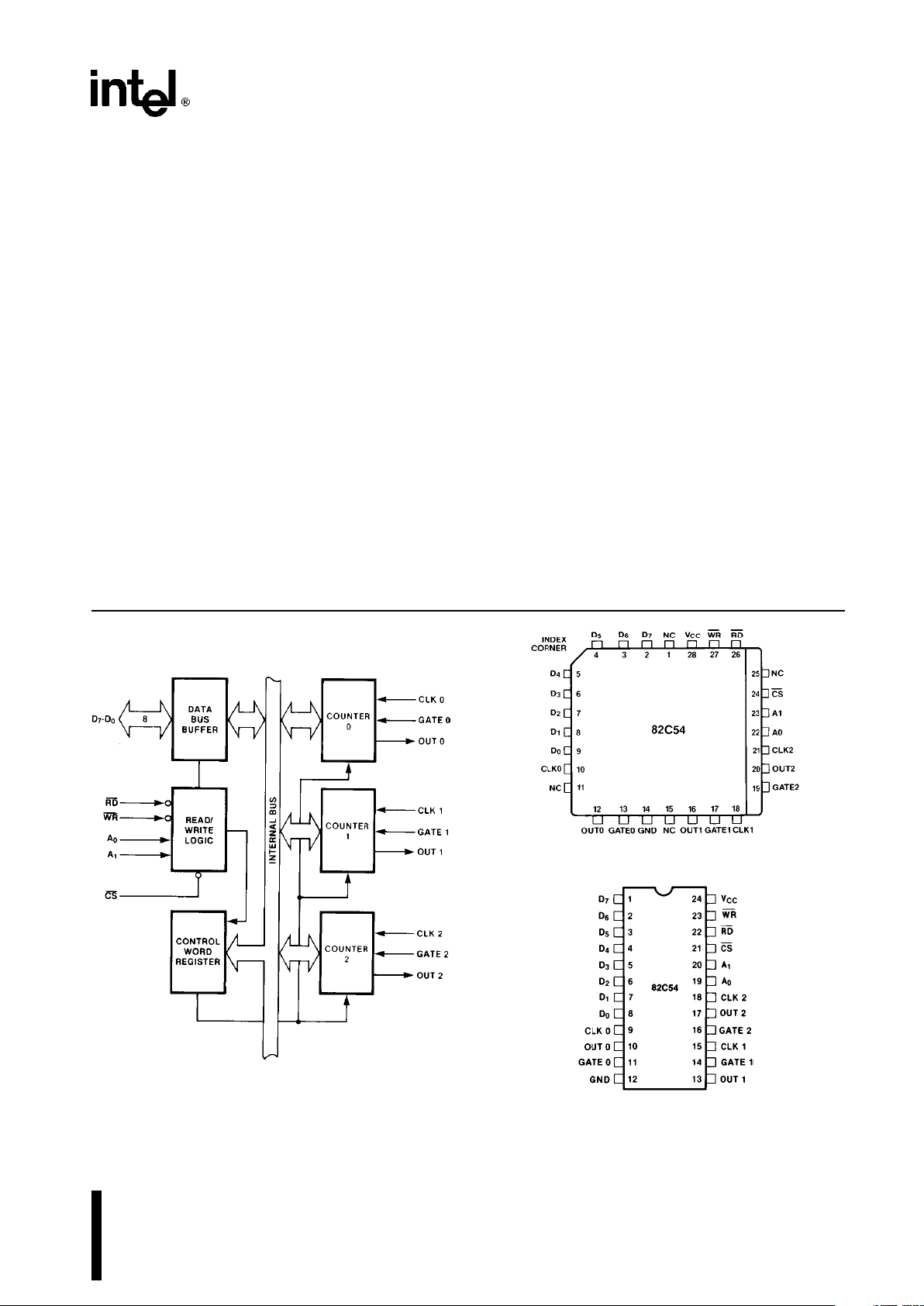
231244–1
Figure 1. 82C54 Block Diagram
231244–3
PLASTIC LEADED CHIP CARRIER
231244–2
Diagrams are for pin reference only.
Package sizes are not to scale.
Figure 2. 82C54 Pinout
82C54
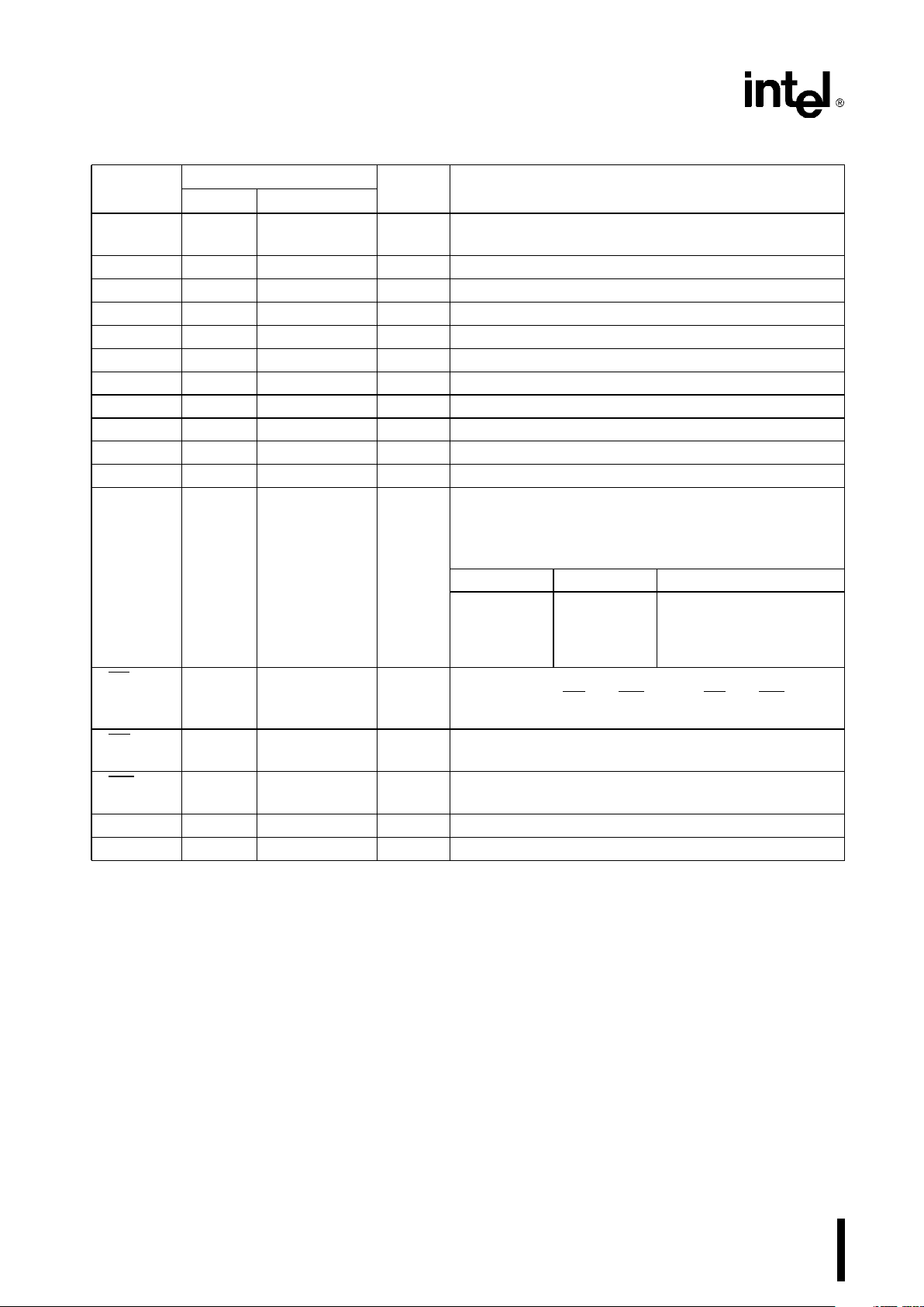
Table 1. Pin Description
Symbol
Pin Number
Type Function
DIP PLCC
D7-D
0
1-8 2-9 I/O Data: Bidirectional tri-state data bus lines,
connected to system data bus.
CLK 0 9 10 I Clock 0: Clock input of Counter 0.
OUT 0 10 12 O Output 0: Output of Counter 0.
GATE 0 11 13 I Gate 0: Gate input of Counter 0.
GND 12 14 Ground: Power supply connection.
OUT 1 13 16 O Out 1: Output of Counter 1.
GATE 1 14 17 I Gate 1: Gate input of Counter 1.
CLK 1 15 18 I Clock 1: Clock input of Counter 1.
GATE 2 16 19 I Gate 2: Gate input of Counter 2.
OUT 2 17 20 O Out 2: Output of Counter 2.
CLK 2 18 21 I Clock 2: Clock input of Counter 2.
A1,A
0
20-19 23-22 I Address: Used to select one of the three Counters
or the Control Word Register for read or write
operations. Normally connected to the system
address bus.
A
1
A
0
Selects
0 0 Counter 0
0 1 Counter 1
1 0 Counter 2
1 1 Control Word Register
CS 21 24 I Chip Select: A low on this input enables the 82C54
to respond to RD
and WR signals. RD and WR are
ignored otherwise.
RD 22 26 I Read Control: This input is low during CPU read
operations.
WR 23 27 I Write Control: This input is low during CPU write
operations.
V
CC
24 28 Power:a5V power supply connection.
NC 1, 11, 15, 25 No Connect
FUNCTIONAL DESCRIPTION
General
The 82C54 is a programmable interval timer/counter
designed for use with Intel microcomputer systems.
It is a general purpose, multi-timing element that can
be treated as an array of I/O ports in the system
software.
The 82C54 solves one of the most common problems in any microcomputer system, the generation
of accurate time delays under software control. Instead of setting up timing loops in software, the programmer configures the 82C54 to match his requirements and programs one of the counters for the de-
sired delay. After the desired delay, the 82C54 will
interrupt the CPU. Software overhead is minimal and
variable length delays can easily be accommodated.
Some of the other counter/timer functions common
to microcomputers which can be implemented with
the 82C54 are:
#
Real time clock
#
Even counter
#
Digital one-shot
#
Programmable rate generator
#
Square wave generator
#
Binary rate multiplier
#
Complex waveform generator
#
Complex motor controller
2
82C54
Block Diagram
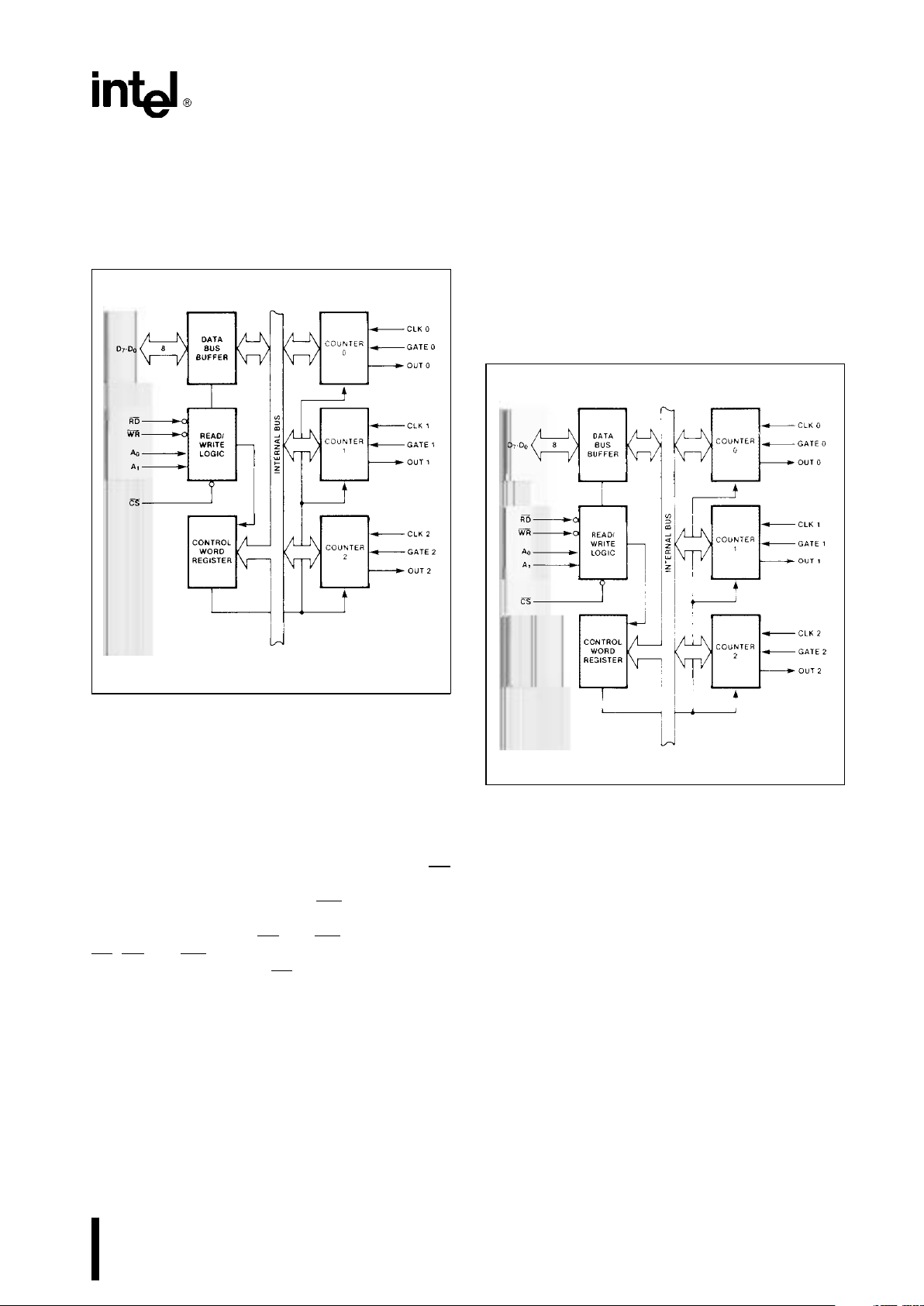
DATA BUS BUFFER
This 3-state, bi-directional, 8-bit buffer is used to interface the 82C54 to the system bus (see Figure 3).
231244–4
Figure 3. Block Diagram Showing Data Bus
Buffer and Read/Write Logic Functions
READ/WRITE LOGIC
The Read/Write Logic accepts inputs from the system bus and generates control signals for the other
functional blocks of the 82C54. A
1
and A0select
one of the three counters or the Control Word Register to be read from/written into. A ‘‘low’’ on the RD
input tells the 82C54 that the CPU is reading one of
the counters. A ‘‘low’’ on the WR
input tells the
82C54 that the CPU is writing either a Control Word
or an initial count. Both RD
and WR are qualified by
CS
;RDand WR are ignored unless the 82C54 has
been selected by holding CS
low.
The WR
Ý
and CLK signals should be synchronous.
This is accomplished by using a CLK input signal to
the 82C54 counters which is a derivative of the system clock source. Another technique is to externally
synchronize the WRÝand CLK input signals. This is
done by gating WR
Ý
with CLK.
CONTROL WORD REGISTER
The Control Word Register (see Figure 4) is selected
by the Read/Write Logic when A
1,A0
e
11. If the
CPU then does a write operation to the 82C54, the
data is stored in the Control Word Register and is
interpreted as a Control Word used to define the
operation of the Counters.
The Control Word Register can only be written to;
status information is available with the Read-Back
Command.
231244–5
Figure 4. Block Diagram Showing Control Word
Register and Counter Functions
COUNTER 0, COUNTER 1, COUNTER 2
These three functional blocks are identical in operation, so only a single Counter will be described. The
internal block diagram of a single counter is shown
in Figure 5.
The Counters are fully independent. Each Counter
may operate in a different Mode.
The Control Word Register is shown in the figure; it
is not part of the Counter itself, but its contents determine how the Counter operates.
3
82C54
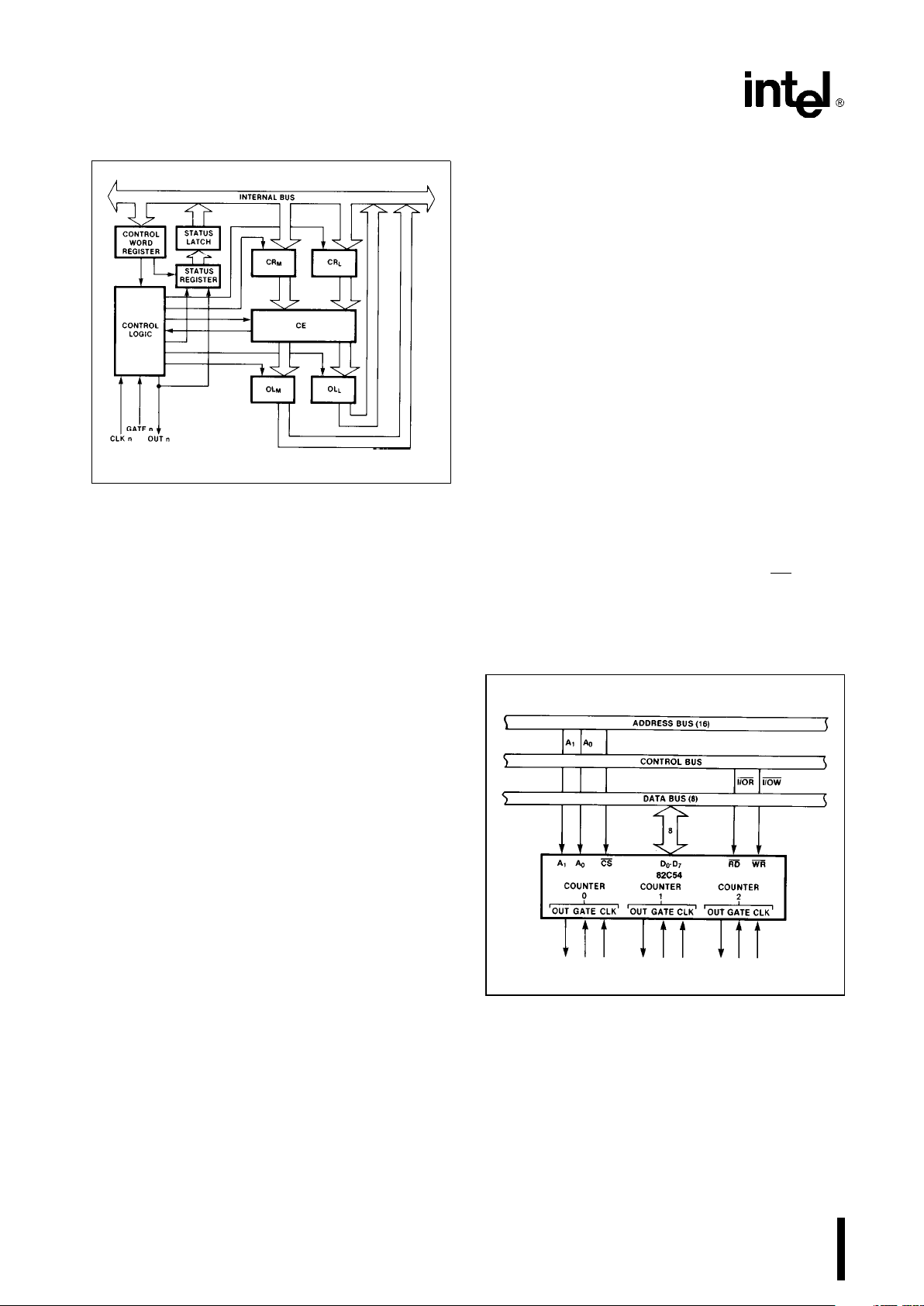
231244–6
Figure 5. Internal Block Diagram of a Counter
The status register, shown in the Figure, when
latched, contains the current contents of the Control
Word Register and status of the output and null
count flag. (See detailed explanation of the ReadBack command.)
The actual counter is labelled CE (for ‘‘Counting Element’’). It is a 16-bit presettable synchronous down
counter.
OL
M
and OLLare two 8-bit latches. OL stands for
‘‘Output Latch’’; the subscripts M and L stand for
‘‘Most significant byte’’ and ‘‘Least significant byte’’
respectively. Both are normally referred to as one
unit and called just OL. These latches normally ‘‘follow’’ the CE, but if a suitable Counter Latch Command is sent to the 82C54, the latches ‘‘latch’’ the
present count until read by the CPU and then return
to ‘‘following’’ the CE. One latch at a time is enabled
by the counter’s Control Logic to drive the internal
bus. This is how the 16-bit Counter communicates
over the 8-bit internal bus. Note that the CE itself
cannot be read; whenever you read the count, it is
the OL that is being read.
Similarly, there are two 8-bit registers called CR
M
and CRL(for ‘‘Count Register’’). Both are normally
referred to as one unit and called just CR. When a
new count is written to the Counter, the count is
stored in the CR and later transferred to the CE. The
Control Logic allows one register at a time to be
loaded from the internal bus. Both bytes are transferred to the CE simultaneously. CR
M
and CRLare
cleared when the Counter is programmed. In this
way, if the Counter has been programmed for one
byte counts (either most significant byte only or least
significant byte only) the other byte will be zero.
Note that the CE cannot be written into; whenever a
count is written, it is written into the CR.
The Control Logic is also shown in the diagram. CLK
n, GATE n, and OUT n are all connected to the outside world through the Control Logic.
82C54 SYSTEM INTERFACE
The 82C54 is treated by the systems software as an
array of peripheral I/O ports; three are counters and
the fourth is a control register for MODE programming.
Basically, the select inputs A
0,A1
connect to the A0,
A
1
address bus signals of the CPU. The CS can be
derived directly from the address bus using a linear
select method. Or it can be connected to the output
of a decoder, such as an Intel 8205 for larger systems.
231244–7
Figure 6. 82C54 System Interface
4
82C54
OPERATIONAL DESCRIPTION
General
After power-up, the state of the 82C54 is undefined.
The Mode, count value, and output of all Counters
are undefined.
How each Counter operates is determined when it is
programmed. Each Counter must be programmed
before it can be used. Unused counters need not be
programmed.
Programming the 82C54
Counters are programmed by writing a Control Word
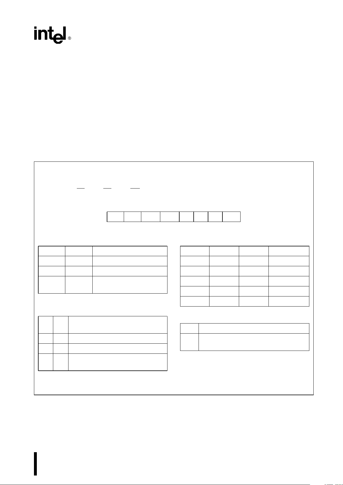
and then an initial count. The control word format is
shown in Figure 7.
All Control Words are written into the Control Word
Register, which is selected when A
1,A0
e
11. The
Control Word itself specifies which Counter is being
programmed.
By contrast, initial counts are written into the Counters, not the Control Word Register. The A
1,A0
inputs are used to select the Counter to be written
into. The format of the initial count is determined by
the Control Word used.
Control Word Format
A1,A
0
e
11 CSe0RDe1WRe0
D
7D6D5D4D3D2D1D0
SC1 SC0 RW1 RW0 M2 M1 M0 BCD
SC Ð Select Counter:
SC1 SC0
0 0 Select Counter 0
0 1 Select Counter 1
1 0 Select Counter 2
11
Read-Back Command
(See Read Operations)
RW Ð Read/Write:
RW1 RW0
0 0 Counter Latch Command (see Read
Operations)
0 1 Read/Write least significant byte only.
1 0 Read/Write most significant byte only.
1 1 Read/Write least significant byte first,
then most significant byte.
NOTE: Don’t care bits (X) should be 0 to insure
compatibility with future Intel products.
M Ð MODE:
M2 M1 M0
0 0 0 Mode 0
0 0 1 Mode 1
X 1 0 Mode 2
X 1 1 Mode 3
1 0 0 Mode 4
1 0 1 Mode 5
BCD:
0 Binary Counter 16-bits
1 Binary Coded Decimal (BCD) Counter
(4 Decades)
Figure 7. Control Word Format
5

82C54
Write Operations
The programming procedure for the 82C54 is very
flexible. Only two conventions need to be remembered:
1) For each Counter, the Control Word must be
written before the initial count is written.
2) The initial count must follow the count format
specified in the Control Word (least significant
byte only, most significant byte only, or least significant byte and then most significant byte).
Since the Control Word Register and the three
Counters have separate addresses (selected by the
A
1,A0
inputs), and each Control Word specifies the
Counter it applies to (SC0, SC1 bits), no special in-
struction sequence is required. Any programming
sequence that follows the conventions above is acceptable.
A new initial count may be written to a Counter at
any time without affecting the Counter’s programmed Mode in any way. Counting will be affected
as described in the Mode definitions. The new count
must follow the programmed count format.
If a Counter is programmed to read/write two-byte
counts, the following precaution applies: A program
must not transfer control between writing the first
and second byte to another routine which also writes
into that same Counter. Otherwise, the Counter will
be loaded with an incorrect count.
A
1
A
0
Control Word Ð Counter 0 1 1
LSB of count Ð Counter 0 0 0
MSB of count Ð Counter 0 0 0
Control Word Ð Counter 1 1 1
LSB of count Ð Counter 1 0 1
MSB of count Ð Counter 1 0 1
Control Word Ð Counter 2 1 1
LSB of count Ð Counter 2 1 0
MSB of count Ð Counter 2 1 0
A
1
A
0
Control Word Ð Counter 0 1 1
Counter Word Ð Counter 1 1 1
Control Word Ð Counter 2 1 1
LSB of count Ð Counter 2 1 0
LSB of count Ð Counter 1 0 1
LSB of count Ð Counter 0 0 0
MSB of count Ð Counter 0 0 0
MSB of count Ð Counter 1 0 1
MSB of count Ð Counter 2 1 0
A
1
A
0
Control Word Ð Counter 2 1 1
Control Word Ð Counter 1 1 1
Control Word Ð Counter 0 1 1
LSB of count Ð Counter 2 1 0
MSB of count Ð Counter 2 1 0
LSB of count Ð Counter 1 0 1
MSB of count Ð Counter 1 0 1
LSB of count Ð Counter 0 0 0
MSB of count Ð Counter 0 0 0
A
1
A
0
Control Word Ð Counter 1 1 1
Control Word Ð Counter 0 1 1
LSB of count Ð Counter 1 0 1
Control Word Ð Counter 2 1 1
LSB of count Ð Counter 0 0 0
MSB of count Ð Counter 1 0 1
LSB of count Ð Counter 2 1 0
MSB of count Ð Counter 0 0 0
MSB of count Ð Counter 2 1 0
NOTE:
In all four examples, all counters are programmed to read/write two-byte counts.
These are only four of many possible programming sequences.
Figure 8. A Few Possible Programming Sequences
Read Operations
It is often desirable to read the value of a Counter
without disturbing the count in progress. This is easily done in the 82C54.
There are three possible methods for reading the
counters: a simple read operation, the Counter
Latch Command, and the Read-Back Command.
Each is explained below. The first method is to perform a simple read operation. To read the Counter,
which is selected with the A1, A0 inputs, the CLK
input of the selected Counter must be inhibited by
using either the GATE input or external logic. Otherwise, the count may be in the process of changing
when it is read, giving an undefined result.
6
 Loading...