Intel Corporation N83930AD3, N83930AD4, N83930AE3, N83930AE4, N80930AD4 Datasheet
...
ADVANCE INFORMATION
COPYRIGHT © INTEL CORPORATION, 1997 February 1997 Order Number: 272917-003
8x930A
x
UNIVERSAL SERIAL BUS
MICROCONTROLLER
The 8x930Ax USB microcontroller is based on an 8xC251Sx microcontroller core. It consists of standard
8
x
C251Sx peripherals plus an added USB function. The 8x930Ax uses the standard instruction set of the
MCS 251 architecture, which is binary code compatible with the MCS 51 architecture. The USB function
integrates the USB transceiver, serial bus interface engine (SIE), function interface unit (FIU) and
transmit/receive FIFOs. The USB function also supports full-speed/low-speed data rates, suspend/resume
modes, isochronous/non-isochronous transfers, and is fully compliant with the USB rev 1.0 specification.
■ Complete Universal Serial Bus
Specification 1.0 Compatibility
—Supports Isochronous and
Non-isochronous Data
—Bidirectional Half-duplex Link
■ On-chip USB Transceiver
■ Serial Bus Interface Engine (SIE)
—Packet Decoding/Generation
—CRC Generation and Checking
—NRZI Encoding/Decoding and
Bit-stuffing
■ USB Reset Interrupt
■ Four Transmit FIFOs
—Three 16-byte FIFOs
—One Configurable FIFO (up to
1 Kbyte)
■ Four Receive FIFOs
—Three 16-byte FIFOs
—One Configurable FIFO (up to
1 Kbyte)
■ Automatic Transmit/Receive FIFO
Management
■ Suspend/Resume Operation
■ Three New USB Interrupt Vectors
— USB Function Interrupt
— Start of Frame
—Suspend/Resume
■ Phase-locked Loop
—12 Mbps or 1.5 Mbps Data Rate
■ Low Clock Mode
■ User-selectable Configurations
—External Wait State
—Address Range
—Page Mode
■ Real-time Wait Function
■ 256-Kbyte External Code/Data Memory
Space
■ On-chip ROM Options
—0, 8, or 16 Kbytes
■ 1 Kbyte On-chip Data RAM
■ Four Input/Output Ports
—1 Open-drain port
— 3 Quasi-bidirectional Ports
■ Programmable Counter Array (PCA)
—5 Capture/Compare Modules
■ Serial I/O Port (UART)
■ Hardware Watchdog Timer
■ Three Flexible 16-bit Timer/Counters
■ Power-saving Idle and Powerdown
Modes
■ Register-based MCS
®
251 Architecture
—40-byte Register File
—Registers Accessible as Bytes,
Words, or Doublewords
■ Code Compatible with MCS 51 and MCS
251 Microcontrollers
■ 6 or 12 MHz Crystal Operation

Information in this document is provided in connection with Intel products. No license, express or implied, by estoppel or oth-
erwise, to a ny intell e ctua l p rop ert y r i ght s is granted by thi s do cum ent . E xce pt as pr ovide d i n I nte l’s T erm s a nd Co nditi o ns of
Sale for such products, Intel assumes no liability whatsoever, and Intel disclaims any express or implied warranty, relating to
sale and/or use of Intel products including liability or warranties relating to fitness for a particular purpose, merchantability, or
infringement of any patent, copyright or other intellectual property right. Intel products are not intended for use in medical, life
saving, or life sustaining applications.
Intel retains the right to make changes to specifications and product descriptions at any time, without notice.
The product may contain design defects or errors known as errata. Current characterized errata are available on request.
*Third-party brands and names are the property of their respective owners.
Contact your local Intel sales office or your distributor to obtain the latest specifications and before placing your product order.
Copies of documents w hich have an order ing numb er and are refer enced in this document, or othe r Intel litera ture, may be
obtained from:
Intel Corporation
Literature Sales
P.O. Box 7641
Mt. Prospect, IL 60056-7641
or call 1-800-548-4725
COPYRIGHT © INTEL CORPORATION, 1997

iii
CONTENTS
1.0 Nomenclature Overview...................................................................................................... 3
2.0 Pinout.................................................................................................................................. 4
3.0 Signals ................................................................................................................................ 7
4.0 Address Map..................................................................................................................... 10
5.0 Electrical Characteristics................................................................................................... 11
5.1 Operating Frequencies.............................................. ...... ...... ....................................... 12
5.2 DC Characteristics........................................................................................................ 13
5.3 Definition of AC Symbols.............................................................................................. 15
5.4 AC Characteristics........................................................................................................ 16
5.4.1 System Bus AC Characteristics ............................................................................16
5.4.2 System Bus Timing Diagrams, Nonpage Mode ....................................................18
5.4.3 System Bus Timing Diagrams, Page Mode ...........................................................20
5.4.4 Definition of Real-time Wait Symbols ....................................................................22
5.4.5 Real-time Wait Function AC Characteristics .........................................................22
5.4.6 Real-Time Wait Function Timing Diagrams ...........................................................23
5.5 AC Characteristics — Serial Port, Synchronous Mode 0............................................. 27
5.6 External Clock Drive..................................................................................................... 28
5.7 Testing Waveforms ...................................................................................................... 29
6.0 Thermal Characteristics.................................................................................................... 30
7.0 Product Reference............................................................................................................ 30
7.1 External Bus Timing and Peripheral Timing Affected by PLLSEL2:0 Selection........... 30
7.2 Low Clock Mode Frequency......................................................................................... 30
7.3 Setting FFRC Bit Clears Only the Oldest Packet in the FIFO...................................... 30
7.4 Series Resistor Requirement for Impedance Matching................................................ 30
7.5 Pullup Requirement for Full Speed Device and Low Speed Device............................. 30
7.6 Powerdown Mode Cannot Be Invoked Before USB Suspend...................................... 30
8.0 Specification Supplement for 8
x
930Ax3 and 8x930Ax4.................................................... 31
8.1 Six Endpoint Pairs Functionality................................................................................... 31
8.2 DC Characteristics........................................................................................................ 31
8.3 Extended Data Float (EDF) AC Timing Feature........................................................... 31
9.0 Device Errata ................................................. ............................ ..... ...... ..... ...... ................. 34
10.0 Datasheet Revision History............................................................................................... 34

8x930Ax UNIVERSAL SERIAL BUS MICROCONTROLLER
iv
Figures
1. 8x930Ax Internal Block Diagram..........................................................................................1
2. USB Module Block Diagram.................................................................................................2
3. Product Nomenclature .........................................................................................................3
4. 8
x
930Ax 68-pin PLCC Package........................................................................................... 4
5. Clock Circuit.......................................................................................................................12
6. 8x930Ax Code Fetch, Nonpage Mode...............................................................................18
7. 8
x
930Ax Data Read, Nonpage Mode ................................................................................19
8. 8
x
930Ax Data Write, Nonpage Mode.................................................................................19
9. 8
x
930Ax Code Fetch, Page Mode .....................................................................................20
10. 8
x
930Ax Data Read, Page Mode.......................................................................................21
11. 8
x
930Ax Data write, Page Mode........................................................................................21
12. External Code Fetch/Data Read (Nonpage Mode, Real-time Wait State) .........................23
13. External Data Write (Nonpage Mode, Real-time Wait State).............................................24
14. External Data Read (Page Mode, Real-time Wait State)...................................................25
15. External Data Write (Page Mode, Real-time Wait State)...................................................26
16. Serial Port Waveform — Synchronous Mode 0..................................................................27
17. External Clock Drive Waveforms........................................................................................28
18. AC Testing Input, Output Waveforms.................................................................................29
19. Float Waveforms................................................................................................................ 29
Tables
1. Description of Product Nomenclature...................................................................................3
2. Proliferation Options.............................................................................................................3
3. 68-pin PLCC Pin Assignment...............................................................................................5
4. 68-pin PLCC Signal Assignments Arranged by Functional Category ..................................6
5. Signal Descriptions ..............................................................................................................7
6. Memory Signal Selections (RD1:0)....................................................................................10
7. 8
x
930Ax Address Map.......................................................................................................10
8. Frequency Selection and Operating Frequency.................................................................12
9. DC Characteristics at Operating Conditions.......................................................................13
10. AC Timing Symbol Definitions............................................................................................15
11. AC Characteristics at Operating Conditions.......................................................................16
12. Real-time Wait Timing Symbol Definitions.........................................................................22
13. Real-time Wait AC Timing Specifications...........................................................................22
14. Serial Port Timing — Synchronous Mode 0.......................................................................27
15. External Clock Drive...........................................................................................................28
16. Thermal Characteristics.....................................................................................................30
17. SIx Endpoint Pair Feature..................................................................................................31
18. Effect of “EDF#” on Wait States.........................................................................................31
19. AC Characteristics for 8x930Ax3 and 8x930Ax4 in Compatibility Mode............................32
20. 8
x
930Ax3 and 8x930Ax4 Default and Extended Data Float Timings................................ .32
21. 8
x
930Ax3 and 8x930Ax4 Real-time Wait State AC Timing Specifications........................33

ADVANCE INFORMATION 1
8x930Ax UNIVERSAL SERIAL BUS (USB) MICROCONTROLLER
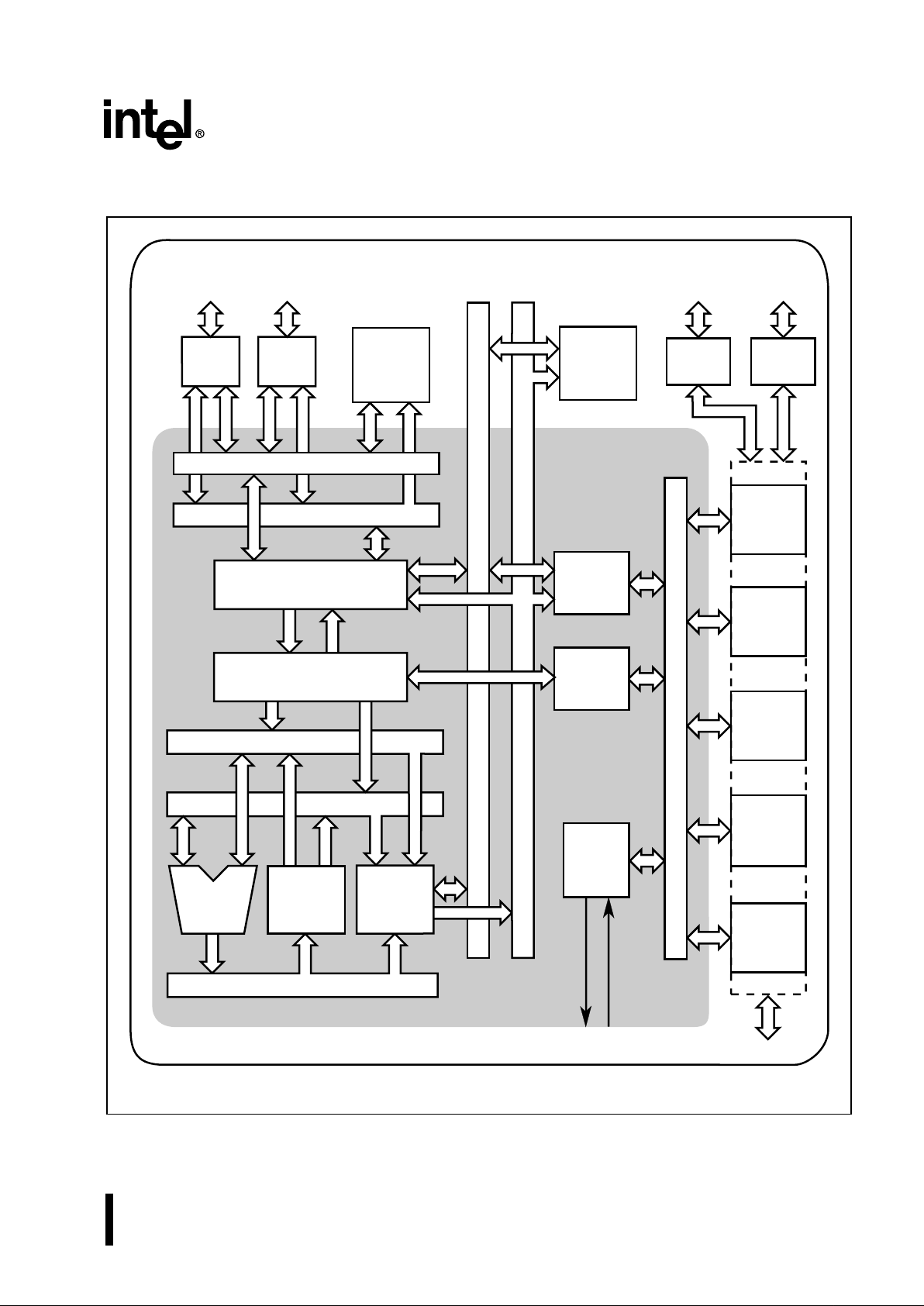
Figure 1. 8x930Ax Internal Block Diagram
A4340-01
SRC2 (8)
Code Address (24)
Code Bus (16)
RAM
ROM
Watchdog
Timer
Timer/
Counters
PCA
Serial I/O
Port 2
Drivers
P2.7:0
Port 0
Drivers
P0.7:0
Port 3
Drivers
P3.7:0
Port 1
Drivers
P1.7:0
Data Address (24)
Data Bus (8)
Memory Address (16)
System Bus and I/O Ports
I/O Ports and
Peripheral Signals
SRC1 (8)
IB Bus (8)
Peripheral
Interface
Interrupt
Handler
Clock
&
Reset
Bus Interface
Instruction Sequencer
DST (16)
ALU
Data
Memory
Interface
Memory Data (16)
Register
File
USB
†
USB Ports
Microcontroller Core
†
For details, see the USB module block diagram.

2 ADVANCE INFORMATION
8x930Ax UNIVERSAL SERIAL BUS (USB) MICROCONTROLLER
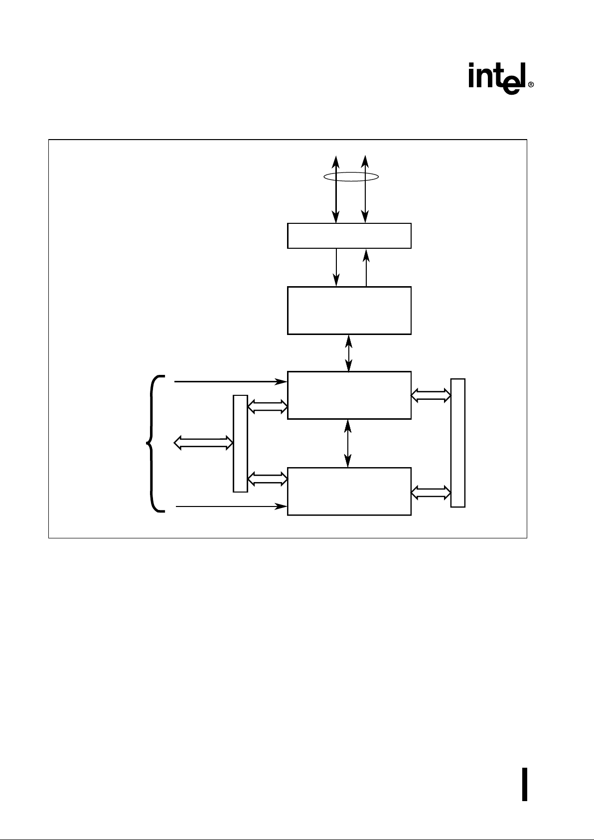
Figure 2. USB Module Block Diagram
D
P0
Transceiver
Control
Control
Control
Transmit/Receive Bus
FIFOs
D
M0
A4231-03
Data Bus
Serial Bus
Interface Engine
(SIE)
Function
Interface Unit
(FIU)
USB
Upstream
Port
To
CPU

ADVANCE INFORMATION 3
8x930Ax UNIVERSAL SERIAL BUS (USB) MICROCONTROLLER
1.0 NOMENCLATURE OVERVIEW
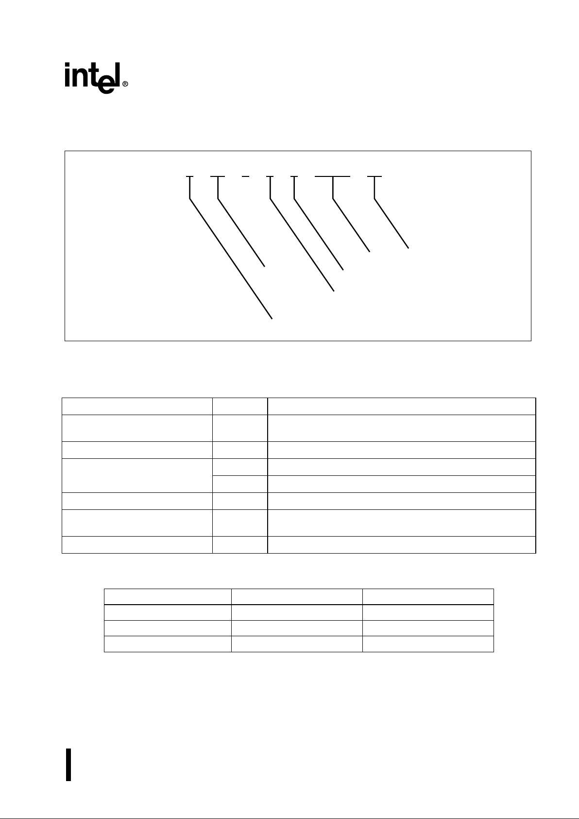
Figure 3. Product Nomenclature
Table 1. Description of Product Nomenclature
Parameter Options Description
Temperature and Burn-in no mark Commercial operating temperature range (0
o
C to 70oC) with
Intel standard burn-in.
Packaging Options N Plastic Leaded Chip Carrier (PLCC)
Program Memory Options 0 Without ROM
3 With ROM
Process and Voltage Information no mark CHMOS
Product Family 930 Advanced 8-bit microcontroller architecture with on-chip Uni-
versal Serial Bus (USB) function peripherals
Device Speed no mark 6 or 12 MHz crystal
Table 2. Proliferation Options
Product Name ROM Size RAM Size
80930AD 0 1 Kbyte
83930AD 8 Kbytes 1 Kbyte
83930AE 16 Kbytes 1 Kbyte
Program Memory Options
XXXXX XXXX8XXX
Packaging Options
Temperature and Burn-in Options
A2815-01
Process Information
Product Family
Device Speed

4 ADVANCE INFORMATION
8x930Ax UNIVERSAL SERIAL BUS (USB) MICROCONTROLLER
2.0 PINOUT
Figure 4. 8x930Ax 68-pin PLCC Package
Figure 4 illustrates the 8
x
930Ax PLCC package.
Table 3 lists the pin assignments by pin number,
and Table 4 lists the pin assignments by functional
categories. Table 5 describes the signals.
Reserved
Reserved
Reserved
Reserved
Reserved
D
P0
D
M0
ECAP
V
SSP
V
CCP
SOF#
Reserved
Reserved
Reserved
Reserved
Reserved
PLLSEL0
A8 / P2.0
A9 / P2.1
A10 / P2.2
A11 / P2.3
A12 / P2.4
A13 / P2.5
A14 / P2.6
A15 / P2.7
V
SSVCC
EA#
ALE
PSEN#
Reserved
Reserved
Reserved
Reserved
A4392-02
AD7 / P0.7
AD6 / P0.6
AD5 / P0.5
AD4 / P0.4
AD3 / P0.3
AD2 / P0.2
AD1 / P0.1
AD0 / P0.0
V
SSP
V
CCP
P3.0 / RXD
P3.1 / TXD
P3.2 / INT0#
P3.3 / INT1#
P3.4 / T0
P3.5 / T1
P3.6 / WR#
60
59
58
57
56
55
54
53
52
51
50
49
48
47
46
45
44
View of component as
mounted on PC board
10
11
12
13
14
15
16
17
18
19
20
21
22
23
24
25
26
P3.7 / RD# / A16
P1.0 / T2
P1.1 / T2EX
P1.2 / ECI
P1.3 / CEX0
P1.4 / CEX1
P1.5 / CEX2
P1.6 / CEX3 / WAIT#
P1.7 / CEX4 / A17 / WCLK
V
CC
V
SS
XTAL1
XTAL2
AV
CC
RST
PLLSEL1
PLLSEL2
27
28
29
30
31
32
33
34
35
36
37
38
39
40
41
42
43
987654321
68
67
66
65
64
63
62
61
Note: Reserved pins must be left unconnected.

ADVANCE INFORMATION 5
8x930Ax UNIVERSAL SERIAL BUS (USB) MICROCONTROLLER
Table 3. 68-pin PLCC Pin Assignment
Pin Name Pin Name Pin Name
1V
SS
24 P3.4/T0 47 Reserved
2 A15/P2.7 25 P3.5/T1 48 Reserved
3 A14/P2.6 26 P3.6/WR# 49 Reserved
4 A13/P2.5 27 P3.7/RD#/A16 50 SOF#
5 A12/P2.4 28 P1.0/T2 51 V
CCP
6 A11/P2.3 29 P1.1/T2EX 52 V
SSP
7 A10/P2.2 30 P1.2/ECI 53 ECAP
8 A9/P2.1 31 P1.3/CEX0 54 D
M0
9 A8/P2.0 32 P1.4/CEX1 55 D
P0
10 AD7/P0.7 33 P1.5/CEX2 56 Reserved
11 AD6/P0.6 34 P1.6/CEX3/WAIT# 57 Reserved
12 AD5/P0.5 35 P1.7/CEX4/A17/WCLK 58 Reserved
13 AD4/P0.4 36 V
CC
59 Reserved
14 AD3/P0.3 37 V
SS
60 Reserved
15 AD2/P0.2 38 XTAL1 61 Reserved
16 AD1/P0.1 39 XTAL2 62 Reserved
17 AD0/P0.0 40 AV
CC
63 Reserved
18 V
SSP
41 RST 64 Reserved
19 V
CCP
42 PLLSEL1 65 PSEN#
20 P3.0/RXD 43 PLLSEL2 66 ALE
21 P3.1/TXD 44 PLLSEL0 67 EA#
22 P3.2/INT0# 45 Reserved 68 V
CC
23 P3.3/INT1# 46 Reserved

6 ADVANCE INFORMATION
8x930Ax UNIVERSAL SERIAL BUS (USB) MICROCONTROLLER
Table 4. 68-pin PLCC Signal Assignments Arranged by Functional Category
Address & Data Input/Output USB
Name Pin Name Pin Name Pin
AD0/P0.0 17 P1.0/T2 28 PLLSEL0 44
AD1/P0.1 16 P1.1/T2EX 29 PLLSEL1 42
AD2/P0.2 15 P1.2/ECI 30 PLLSEL2 43
AD3/P0.3 14 P1.3/CEX0 31 SOF# 50
AD4/P0.4 13 P1.4/CEX1 32 ECAP 53
AD5/P0.5 12 P1.5/CEX2 33 D
M0
54
AD6/P0.6 11 P1.6/CEX3/WAIT# 34 D
P0
55
AD7/P0.7 10 P1.7/CEX4/A17/WCLK 35
A8/P2.0 9 P3.0/RXD 20 Processor Control
A9/P2.1 8 P3.1/TXD 21 Name Pin
A10/P2.2 7 P3.4/T0 24 P3.2/INT0# 22
A11/P2.3 6 P3.5/T1 25 P3.3/INT1# 23
A12/P2.4 5 EA# 67
A13/P2.5 4 Bus Control & Status RST 41
A14/P2.6 3 Name Pin XTAL1 38
A15/P2.7 2 P3.6/WR# 26 XTAL2 39
P3.7/RD#/A16 27 P3.7/RD#/A16 27
P1.7/CEX4/A17/WCLK 35 ALE 66
PSEN# 65
Power & Ground
Name Pin
V
CC
36, 68
V
CCP
19, 51
AV
CC
40
EA# 67
V
SS
1, 37
V
SSP
18, 52

ADVANCE INFORMATION 7
8x930Ax UNIVERSAL SERIAL BUS (USB) MICROCONTROLLER
3.0 SIGNALS
Table 5. Signal Descriptions
Signal
Name
Type Description Alternate Function
A17 O 18th Address Bit (A17). Output to memory as 18th exter-
nal address bit (A17) in extended bus applications, depending on the values of bits RD0 and RD1 in configuration byte
UCONFIG0. See also RD#, PSEN#.
P1.7/CEX4/WCLK
A16 O Address Line 16. See RD#. RD#
A15:8
†
O Address Lines. Upper address lines for the external bus. P2.7:0
AD7:0
†
I/O Address/Data Lines. Multiplexed lower address lines and
data lines for external memory.
P0.7:0
ALE O Address Latch Enable (ALE). ALE signals the start of an
external bus cycle and indicates that valid address information is available on lines A15:8 and AD7:0. An external latch
can use ALE to demultiplex the address from the
address/data bus.
PROG#
AV
CC
PWR Analog VCC. A separate VCC input for the phase-locked loop
circuitry.
CEX2:0
CEX3
CEX4
I/O Programmable Counter Array (PCA) Input/Output Pins.
These are input signals for the PCA capture mode and output signals for the PCA compare mode and PCA PWM
mode.
P1.5:3
P1.6/WAIT#
P1.7/A17/WCLK
D
M0
I/O Data Minus. USB minus data line interface. —
D
P0
I/O Data Plus. USB plus data line interface. —
EA# I External Access. Directs program memory accesses to
on-chip or off-chip code memory. For EA# strapped to
ground, all program memory accesses are off-chip. For EA#
strapped to V
CC
, program accesses on-chip ROM if the
address is within the range of the on-chip ROM; otherwise,
the access is off-chip. The value of EA# is latched at reset.
For devices without on-chip ROM, EA# must be strapped to
ground.
ECAP I External Capacitor. Must be connected to a 1 µF capacitor
(or larger) to ensure proper operation of the differential line
driver. The other lead of the capacitor must be connected to
V
SS
.
ECI I PCA External Clock Input. External clock input to the 16-
bit PCA timer.
P1.2
INT1:0# I External Interrupts 0 and 1. These inputs set bits IE1:0 in
the TCON register. If bits IT1:0 in the TCON register are
set, bits IE1:0 are set by a falling edge on INT1#/INT0#. If
bits INT1:0 are clear, bits IE1:0 are set by a low level on
INT1:0#.
P3.3:2
P0.7:0 I/O Port 0. This is an 8-bit, open-drain, bidirectional I/O port. AD7:0
†
The descriptions of A15:8/P2.7:0 and AD7:0/P0.7:0 are for the nonpage-mode chip configuration. If the
chip is configured for page-mode operation, port 0 carries the lower address bits (A7:0), and port 2 carries the upper address bits (A15:8) and the data (D7:0).

8 ADVANCE INFORMATION
8x930Ax UNIVERSAL SERIAL BUS (USB) MICROCONTROLLER
P1.0
P1.1
P1.2
P1.5:3
P1.6
P1.7
I/O Port 1. This is an 8-bit, bidirectional I/O port with internal
pullups.
T2
T2EX
ECI
CEX2:0
CEX3/WAIT#
CEX4/A17/WCLK
P2.7:0 I/O Port 2. This is an 8-bit, bidirectional I/O port with internal
pullups.
A15:8
P3.0
P3.1
P3.3:2
P3.5:4
P3.6
P3.7
I/O Port 3. This is an 8-bit, bidirectional I/O port with internal
pullups.
RXD
TXD
INT1:0#
T1:0
WR#
RD#/A16
PLLSEL2:0 I Phase-locked Loop Select. Three-bit code selects USB
data rate (see Table 8 on page 12).
—
PSEN# O Program Store Enable. Read signal output. This output is
asserted for a memory address range that depends on bits
RD0 and RD1 in configuration byte UCONFIG0 (see RD#).
—
RD# O Read or 17th Address Bit (A16). Read signal output to
external data memory or 17th external address bit (A16),
depending on the values of bits RD0 and RD1 in configuration byte UCONFIG0 (See PSEN#).
P3.7/A16
RST I Reset. Reset input to the chip. Holding this pin high for 64
oscillator periods while the oscillator is running resets the
device. The port pins are driven to their reset conditions
when a voltage greater than V
IH1
is applied, whether or not
the oscillator is running. This pin has an internal pulldown
resistor which allows the device to be reset by connecting a
capacitor between this pin and V
CC
.
Asserting RST when the chip is in idle mode or powerdown
mode returns the chip to normal operation.
—
RXD I /O Receive Serial Data. RXD sends and receives data in
serial I/O mode 0 and receives data in serial I/O modes 1, 2,
and 3.
P3.0
SOF# O Start of Frame. Start of Frame pulse. Active low, asserted
for 8 states (see Table 8 on page 12 for state versus XTAL
clock) when Frame Timer is locked to USB frame timing
and SOF token or artificial SOF is detected.
—
T1:0 I Timer 1:0 External Clock Inputs. When timer 1:0 operates
as a counter, a falling edge on the T1:0 pin increments the
count.
P3.5:4
T2 I/O Timer 2 Clock Input/Output. For the timer 2 capture mode,
this signal is the external clock input. For the clock-out
mode, it is the timer 2 clock output.
P1.0
Table 5. Signal Descriptions (Continued)
Signal
Name
Type Description Alternate Function
†
The descriptions of A15:8/P2.7:0 and AD7:0/P0.7:0 are for the nonpage-mode chip configuration. If the
chip is configured for page-mode operation, port 0 carries the lower address bits (A7:0), and port 2 carries the upper address bits (A15:8) and the data (D7:0).
 Loading...