Intel Corporation N386SX, N387SX Datasheet
*Other brands and names are the property of their respective owners.
Information in this document is provided in connection with Intel products. Intel assumes no liability whatsoever, including infringement of any patent or
copyright, for sale and use of Intel products except as provided in Intel’s Terms and Conditions of Sale for such products. Intel retains the right to make
changes to these specifications at any time, without notice. Microcomputer Products may have minor variations to this specification known as errata.
January 1994
COPYRIGHT
©
INTEL CORPORATION, 1995
Order Number: 240225-009
Intel387TMSX
MATH COPROCESSOR
Y
New Automatic Power Management
Ð Low Power Consumption
Ð Typically 100 mA in Dynamic Mode,
and 4 mA in Idle Mode
Y
Socket Compatible with Intel387 Family
of Math CoProcessors
Ð Hardware and Software Compatible
Ð Supported by Over 2100 Commercial
Software Packages
Ð 10% to 15% Performance Increase
on Whetstone and Livermore
Benchmarks
Y
Compatible with the Intel386TMSX
Microprocessor
Ð Extends CPU Instruction Set to
Include Trigonometric, Logarithmic,
and Exponential
Y
High Performance 80-Bit Internal
Architecture
Y
Implements ANSI/IEEE Standard
754-1985 for Binary Floating-Point
Arithmetic
Y
Available in a 68-Pin PLCC Package
See Intel Packaging Specification, OrderÝ231369
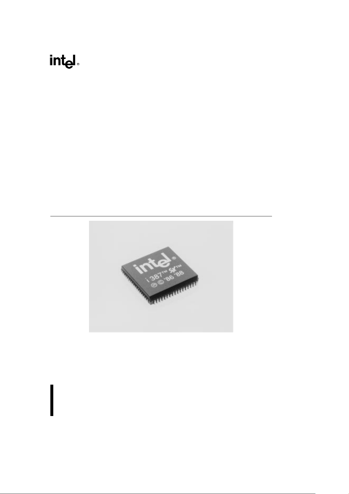
The Intel387TMSX Math CoProcessor is an extension to the Intel386TMSX microprocessor architecture. The
combination of the Intel387
TM
SX with the Intel386TMSX microprocessor dramatically increases the processing speed of computer application software that utilizes high performance floating-point operations. An internal
Power Management Unit enables the Intel387
TM
SX to perform these floating-point operations while maintaining very low power consumption for portable and desktop applications. The internal Power Management Unit
effectively reduces power consumption by 95% when the device is idle.
The Intel387
TM
SX Math CoProcessor is available in a 68-pin PLCC package, and is manufactured on Intel’s
advanced 1.0 micron CHMOS IV technology.
240225– 22
Intel386 and Intel387 are trademarks of Intel Corporation.
1

Intel387TMSX Math CoProcessor
CONTENTS PAGE
1.0 PIN ASSIGNMENT
ААААААААААААААААААААА 5
1.1 Pin Description Table АААААААААААААААА 6
2.0 FUNCTIONAL DESCRIPTION ААААААААА 7
2.1 Feature List ААААААААААААААААААААААААА 7
2.2 Math CoProcessor Architecture АААААА 7
2.3 Power Management ААААААААААААААААА 8
2.3.1 Dynamic Mode ААААААААААААААААА 8
2.3.2 Idle Mode АААААААААААААААААААААА 8
2.4 Compatibility АААААААААААААААААААААААА 8
2.5 Performance АААААААААААААААААААААААА 8
3.0 PROGRAMMING INTERFACE ААААААААА 9
3.1 Instruction Set ААААААААААААААААААААААА 9
3.1.1 Data Transfer Instructions АААААА 9
3.1.2 Arithmetic Instructions АААААААААА 9
3.1.3 Comparison Instructions ААААААА 10
3.1.4 Transcendental
Instructions
ААААААААААААААААААААААА 10
3.1.5 Load Constant Instructions ÀÀÀÀ 10
3.1.6 Processor Instructions ААААААААА 11
3.2 Register Set АААААААААААААААААААААААА 11
3.2.1 Status Word (SW) Register ÀÀÀÀ 12
3.2.2 Control Word (CW)
Register АААААААААААААААААААААААААА 15
3.2.3 Data Register АААААААААААААААААА 16
3.2.4 Tag Word (TW) Register ААААААА 16
3.2.5 Instruction and Data
Pointers
АААААААААААААААААААААААААА 16
3.3 Data Types ААААААААААААААААААААААААА 18
3.4 Interrupt Description АААААААААААААААА 18
3.5 Exception Handling ААААААААААААААААА 18
3.6 Initialization АААААААААААААААААААААААА 21
3.7 Processing Modes АААААААААААААААААА 21
3.8 Programming Support АААААААААААААА 21
CONTENTS PAGE
4.0 HARDWARE SYSTEM
INTERFACE
АААААААААААААААААААААААААААА 21
4.1 Signal Description АААААААААААААААААА 22
4.1.1 Intel386 CPU Clock 2
(CPUCLK2)
ААААААААААААААААААААААА 22
4.1.2 Intel387 Math CoProcessor
Clock 2 (NUMCLK2)
АААААААААААААА 22
4.1.3 Clocking Mode (CKM) ААААААААА 23
4.1.4 System Reset (RESETIN) АААААА 23
4.1.5 Processor Request
(PEREQ) ААААААААААААААААААААААААА 23
4.1.6 Busy Status (BUSYÝ) ААААААААА 23
4.1.7 Error Status (ERRORÝ) ААААААА 23
4.1.8 Data Pins (D15 –D0) ААААААААААА 23
4.1.9 Write/Read Bus Cycle
(W/RÝ) АААААААААААААААААААААААААА 23
4.1.10 Address Stobe (ADSÝ) ААААААА 23
4.1.11 Bus Ready Input
(READY
Ý
) ААААААААААААААААААААААА 24
4.1.12 Ready Output
(READYOÝ) АААААААААААААААААААААА 24
4.1.13 Status Enable (STEN) АААААААА 24
4.1.14 Math CoProcessor Select 1
(NPS1
Ý
) ААААААААААААААААААААААААА 24
4.1.15 Math CoProcessor Select 2
(NPS2) ААААААААААААААААААААААААААА 24
4.1.16 Command (CMD0Ý) ААААААААА 24
4.1.17 System Power (VCC) ААААААААА 24
4.1.18 System Ground (VSS) АААААААА 24
4.2 System Configuration ААААААААААААААА 25
4.3 Math CoProcessor Architecture ААААА 26
4.3.1 Bus Control Logic АААААААААААААА 26
4.3.2 Data Interface and Control
Unit
ААААААААААААААААААААААААААААААА 26
4.3.3 Floating Point Unit ААААААААААААА 26
4.3.4 Power Management Unit ААААААА 26
2
2

CONTENTS PAGE
4.4 Bus Cycles
ААААААААААААААААААААААААА 26
4.4.1 Intel387 SX Math
CoProcessor Addressing АААААААААА 27
4.4.2 CPU/Math CoProcessor
Synchronization ААААААААААААААААААА 27
4.4.3 Synchronous/Asynchronous
Modes АААААААААААААААААААААААААААА 27
4.4.4 Automatic Bus Cycle
Termination
ААААААААААААААААААААААА 27
5.0 BUS OPERATION АААААААААААААААААААА 27
5.1 Non-pipelined Bus Cycles АААААААААА 28
5.1.1 Write Cycle АААААААААААААААААААА 28
5.1.2 Read Cycle АААААААААААААААААААА 29
5.2 Pipelined Bus Cycles ААААААААААААААА 29
5.3 Mixed Bus Cycles АААААААААААААААААА 30
5.4 BUSYÝand PEREQ Timing
Relationship ААААААААААААААААААААААААА 32
6.0 PACKAGE SPECIFICATIONS АААААААА 33
6.1 Mechanical Specifications АААААААААА 33
6.2 Thermal Specifications ААААААААААААА 33
CONTENTS PAGE
7.0 ELECTRICAL
CHARACTERISTICS
ААААААААААААААААААА 33
7.1 Absolute Maximum Ratings ААААААААА 33
7.2 D.C. Characteristics АААААААААААААААА 34
7.3 A.C. Characteristics АААААААААААААААА 35
8.0 Intel387 SX MATH COPROCESSOR
INSTRUCTION SET
АААААААААААААААААААА 41
APPENDIX AÐIntel387 SX MATH
COPROCESSOR COMPATIBILITY
ÀÀÀÀ A-1
A.1 8087/80287 Compatibility ААААААААА A-1
A.1.1 General Differences АААААААААА A-1
A.1.2 Exceptions ААААААААААААААААААА A-2
APPENDIX BÐCOMPATIBILITY
BETWEEN THE 80287 AND 8087
MATH COPROCESSOR
ААААААААААААААА B-1
3
3

CONTENTS PAGE
FIGURES
Figure 1-1 Intel387 SX Math
CoProcessor Pinout
ААААААААААА 5
Figure 2-1 Intel387 SX Math
CoProcessor Block
Diagram
АААААААААААААААААААААА 7
Figure 3-1 Intel 386 SX CPU and
Intel387 Math CoProcessor
Register Set
ААААААААААААААААА 11
Figure 3-2 Status Word ААААААААААААААААА 12
Figure 3-3 Control Word АААААААААААААААА 15
Figure 3-4 Tag Word Register ААААААААААА 16
Figure 3-5 Instruction and Data Pointer
Image in Memory, 32-Bit
Protected Mode Format
АААААА 17
Figure 3-6 Instruction and Data Pointer
Image in Memory, 16-Bit
Protected Mode Format
АААААА 17
Figure 3-7 Instruction and Data Pointer
Image in Memory, 32-Bit
Real Mode Format
ААААААААААА 17
Figure 3-8 Instruction and Data Pointer
Image in Memory, 16-Bit
Real Mode Format
ААААААААААА 18
Figure 4-1 Intel386 SX CPU and
Intel387 SX Math
CoProcessor System
Configuration
АААААААААААААААА 25
Figure 5-1 Bus State Diagram ААААААААААА 28
Figure 5-2 Non-Pipelined Read and
Write Cycles
ААААААААААААААААА 29
Figure 5-3 Fastest Transition to and
from Pipelined Cycles
АААААААА 30
Figure 5-4 Pipelined Cycles with Wait
States ААААААААААААААААААААААА 31
Figure 5-5 BUSYÝand PEREQ Timing
Relationship ААААААААААААААААА 32
Figure 7-1a Typical Output Valid Delay
vs Load Capacitance at Max
Operating Temperature АААААА 37
Figure 7-1b Typical Output Slew Time vs
Load Capacitance at Max
Operating Temperature
АААААА 37
Figure 7-1c Maximum ICCvs
Frequency ААААААААААААААААААА 37
CONTENTS PAGE
Figure 7-2 CPUCLK2/NUMCLK2
Waveform and
Measurement Points for
Input/Output
ААААААААААААААААА 38
Figure 7-3 Output Signals ААААААААААААААА 38
Figure 7-4 Input and I/O Signals АААААААА 39
Figure 7-5 RESET Signal АААААААААААААААА 39
Figure 7-6 Float from STEN ААААААААААААА 40
Figure 7-7 Other Parameters АААААААААААА 40
TABLES
Table 1-1 Pin Cross ReferenceÐ
Functional Grouping
ААААААААААА 5
Table 3-1 Condition Code
Interpretation ААААААААААААААААА 13
Table 3-2 Condition Code Interpretation
after FPREM and FPREM1
Instructions ААААААААААААААААААА 14
Table 3-3 Condition Code Resulting
from Comparison ААААААААААААА 14
Table 3-4 Condition Code Defining
Operand Class ААААААААААААААА 14
Table 3-5 Mapping Condition Codes to
Intel386 CPU Flag Bits
АААААААА 14
Table 3-6 Intel387 SX Math
CoProcessor Data Type
Representation in Memory
ÀÀÀÀ 19
Table 3-7 CPU Interrupt Vectors
Reserve for Math
CoProcessor
ААААААААААААААААА 20
Table 3-8 Intel387 SX Math
CoProcessor Exceptions АААААА 20
Table 4-1 Pin Summary ААААААААААААААААА 22
Table 4-2 Output Pin Status during
Reset АААААААААААААААААААААААА 23
Table 4-3 Bus Cycle Definition АААААААААА 26
Table 6-1 Thermal Resistances
(§C/Watt) iJCand i
JA
АААААААА 33
Table 6-2 Maximum TAat Various
Airflows АААААААААААААААААААААА 33
Table 7-1 D.C. Specifications ААААААААААА 34
Table 7-2a Timing Requirements of the
Bus Interface Unit АААААААААААА 35
Table 7-2b Timing Requirements of the
Execution Unit АААААААААААААААА 36
Table 7-2c Other AC Parameters ААААААААА 36
Table 8-1 Instruction Formats ААААААААААА 41
4
4
Intel387TMSX MATH COPROCESSOR
1.0 PIN ASSIGNMENT
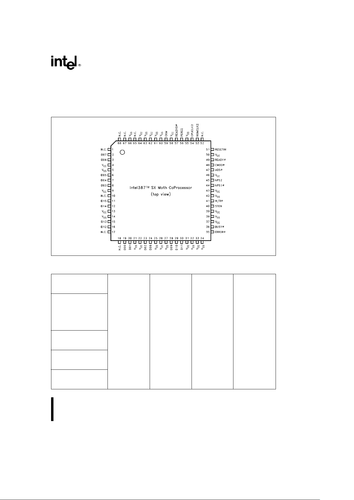
The Intel387 SX Math CoProcessor pinout as
viewed from the top side of the component is shown
in Figure 1-1. V
CC
and VSS(GND) connections must
be made to multiple pins. The circuit board should
include V
CC
and VSSplanes for power distribution
and all V
CC
and VSSpins must be connected to the
appropriate plane.
NOTE:
Pins identified as N.C. should remain completely
unconnected.
240225– 1
Figure 1-1. Intel387TMSX Math CoProcessor Pinout
Table 1-1. Pin Cross ReferenceÐFunctional Grouping
BUSY
Ý
36 D00 19 V
CC
4VSS5 N.C. 1
PEREQ 56 D01 20 9 14 10
ERROR
Ý
35 D02 23 13 21 17
D03 8 22 25 18
ADS
Ý
47
D04 7 26 27 52
CMD0
Ý
48
D05 6 31 32 65
NPS1
Ý
44
D06 3 33 34 67
NPS2 45
D07 2 37 38 68
STEN 40
D08 24 39 42
W/R
Ý
41
D09 28 43 55
READY
Ý
49
D10 29 46 60
READYO
Ý
57
D11 30 50 61
D12 16 58 63
D13 15 62 66
CKM 59
D14 12 64
CPUCLK2 54
D15 11
NUMCLK2 53
RESETIN 51
5
5

Intel387TMSX MATH COPROCESSOR
1.1 Pin Description Table
The following table lists a brief description of each
pin on the Intel387 SX Math CoProcessor. For a
more complete description refer to Section 4.1 Signal Description. The following definitions are used in
these descriptions:
Ý
The signal is active LOW.
I Input Signal
O Output Signal
I/O Input and Output Signal
Symbol Type Name and Function
ADS
Ý
I ADDRESS STROBE indicates that the address and bus cycle definition is valid.
BUSY
Ý
O BUSY indicates that the Math CoProcessor is currently executing an instruction.
CKM I CLOCKING MODE is used to select synchronous or asynchronous clock modes.
CMD0 I COMMAND determines whether an opcode or operand are being sent to the Math
CoProcessor. During a read cycle it indicates which register group is being read.
CPUCLK2 I CPU CLOCK input provides the timing for the bus interface unit and the execution
unit in synchronous mode.
D15–D0 I/O DATA BUS is used to transfer instructions and data between the Math
CoProcessor and CPU.
ERROR
Ý
O ERROR signals that an unmasked exception has occurred.
NC Ð NO CONNECT should always remain unconnected. Connection of a N.C. pin may
cause the Math CoProcessor to malfunction or be incompatible with future
steppings.
NPS1
Ý
I NPX SELECT 1 is used to select the Math CoProcessor.
NPS2 I NPX SELECT 2 is used to select the Math CoProcessor.
NUMCLK2 I NUMERICS CLOCK is used in asynchronous mode to drive the Floating Point
Execution Unit.
PEREQ O PROCESSOR EXTENSION REQUEST signals the CPU that the Math
CoProcessor is ready for data transfer to/from its FIFO.
READY
Ý
I READY indicates that the bus cycle is being terminated.
READYO
Ý
O READY OUT signals the CPU that the Math CoProcessor is terminating the bus
cycle.
RESETIN I SYSTEM RESET terminates any operation in progress and forces the Math
CoProcessor to enter a dormant state.
STEN I STATUS ENABLE serves as a master chip select for the Math CoProcessor.
When inactive, this pin forces all outputs and bi-directional pins into a floating
state.
W/R
Ý
I WRITE/READ indicates whether the CPU bus cycle in progress is a read or a write
cycle.
V
CC
I SYSTEM POWER provides thea5V nominal D.C. supply input.
V
SS
I SYSTEM GROUND provides the 0V connection from which all inputs and outputs
are measured.
6
6
Intel387TMSX MATH COPROCESSOR
2.0 FUNCTIONAL DESCRIPTION
The Intel387 SX Math CoProcessor is designed to
support the Intel386 SX Microprocessor and effectively extend the CPU architecture by providing fast
execution of arithmetic instructions and transcendental functions. This component contains internal
power management circuitry for reduced active power dissipation and an automatic idle mode.
2.1 Feature List
#
New power saving design provides low power
dissipation in active and idle modes.
#
Higher Performance, 10%– 25% higher benchmark performance than the original Intel387 SX
Math CoProcessor.
#
High Performance 84-bit Internal Architecture
#
Eight 80-bit Numeric Registers, usable as individually addressable general registers or as a register stack.
#
Full-range transcendental operations for SINE,
COSINE, TANGENT, ARCTANGENT, and LOGARITHM.
#
Programmable rounding modes and notification
of rounding effects.
#
Exception reporting either by software polling or
hardware interrupts.
#
Fully compatible with the SX Microprocessors.
#
Expands Intel386 SX CPU data types to include
32-bit, 64-bit, and 80-bit Floating Point; 32-bit and
64-bit Integers; and 18 Digit BCD Operands.
#
Directly extends the Intel386 SX CPU Instruction
Set to trigonometric, logarithmic, exponential,
and arithmetic functions for all data types.
#
Operates independently of Real, Protected, and
Virtual-86 Modes of the Intel386 SX Microprocessors.
#
Fully compatible with the Intel387 SL Mobile and
DX Math CoProcessors. Implements all Intel387
Math CoProcessor architectural enhancements
over 8087 and 80287.
#
Implements ANSI/IEEE Standard 754-1985 for
binary floating point arithmetic.
#
Upward Object Code compatible from 8087 and
80287.
2.2 Math CoProcessor Architecture
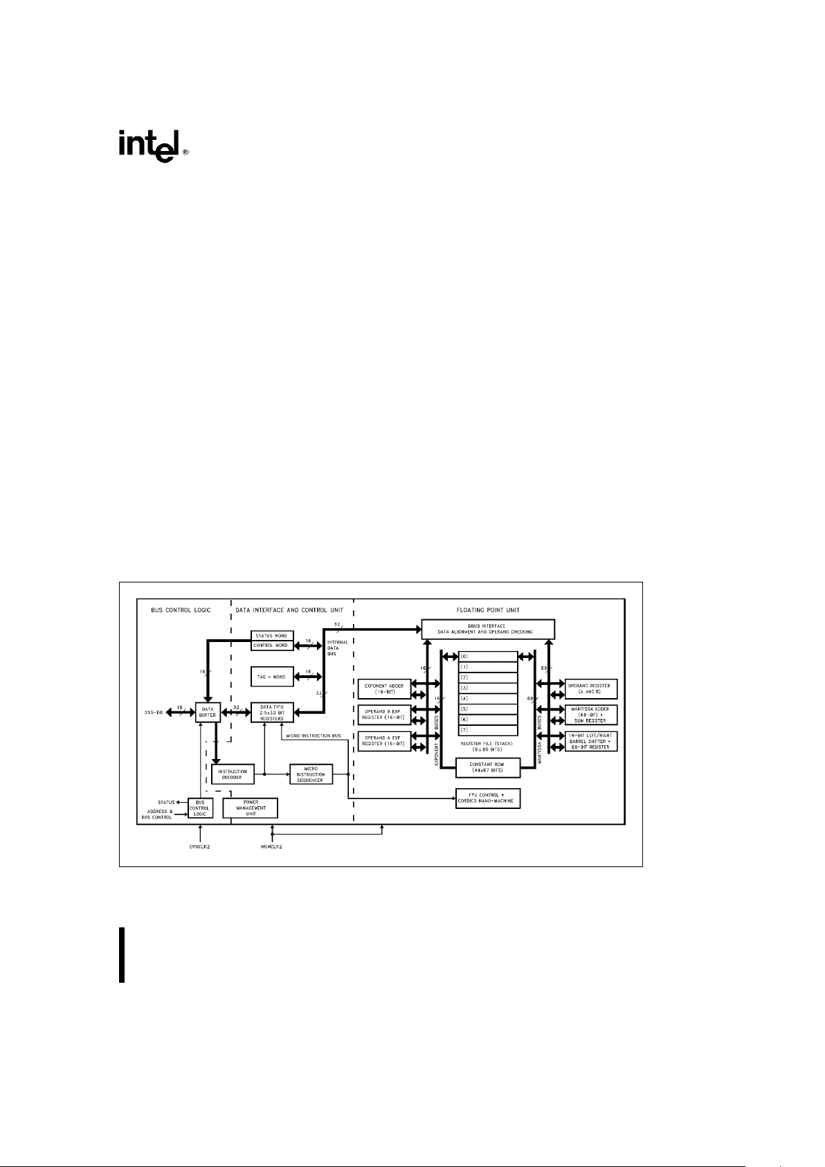
As shown in Figure 2-1, the Intel387 SX Math CoProcessor is internally divided into four sections; the
Bus Control Logic, the Data Interface and Control
Logic, the Floating Point Unit, and the Power Management Unit. The Bus Control Logic is responsible
for the CPU bus tracking and interface. The Data
Interface and Control Unit latches data and decodes
instructions. The Floating Point Unit executes the
mathematical instructions. The Power Management
Unit is new to the Intel387 family and is the nucleus
240225– 2
Figure 2-1. Intel387TMSX Math CoProcessor Block Diagram
7
7

Intel387TMSX MATH COPROCESSOR
of the static architecture. It is responsible for shutting down idle sections of the device to save power.
Microprocessor/Math CoProcessor Interface
The Intel386 CPU interprets the pattern 11011B in
most significant five bits of an instruction as an opcode intended for a math coprocessor. Instructions
thus marked are called ESCAPE or ESC instructions. Upon decoding the instruction as an ESC instruction, the Intel386 CPU transfers the opcode to
the math coprocessor through an I/O write cycle at
a dedicated address (8000F8H) outside the normal
programmed I/O address range. The math coprocessor has dedicated output signals for controlling
the data transfer and notifying the CPU if the Math
CoProcessor is busy or that a floating point error has
occurred.
2.3 Power Management
The Intel387 SX Math CoProcessor offers two
modes of power management; dynamic and idle.
2.3.1 DYNAMIC MODE
Dynamic Mode
is when the device is executing an
instruction. Using Intel’s CHMOS IV technology, the
Intel387 SX Math CoProcessor draws considerably
less power than its predecessor. The active power
supply current is reduced to approximately 100 mA
at 20 MHz and provides low case temperatures.
2.3.2 IDLE MODE
When an instruction is not being executed, the
Intel387 SX Math CoProcessor will automatically
change to
Idle Mode
. Three clocks after completion
of the previous instruction, the internal power manager shuts down the floating point execution unit
and all non-essential circuitry. Only portions of the
Bus Interface Unit remain active to monitor the CPU
bus activity and to accept the next instruction when
it is transferred. When the CPU transfers the next
instruction to the Math CoProcessor, the Intel387 SX
Math CoProcessor accepts the instruction and
ramps the internal core within one clock so there is
no impact to performance or throughput. In idle
mode, the Intel387 SX Math CoProcessor draws typically 4 mA of current and reduces case temperature
to near ambient.
NOTE:
In asynchronous clock mode (CKM
e
0), the inter-
nal idle mode is disabled.
2.4 Compatibility
The Intel387 SX Math CoProcessor is compatible
with the Intel387 SL Mobile Math CoProcessor. Due
to the increased performance and internal pipelining
effects, diagnostic programs should never use instruction execution time for test purposes.
2.5 Performance
The increased performance of floating point calculations can be attributed to the 84-bit architecture and
floating point processor. For the CPU to execute
floating point calculations requires very long software emulation methods with reduced resolution
and accuracy. The performance of the Intel387 SX
Math CoProcessor has been further enhanced
through improvements in the internal microcode and
through internal architectural changes. These refinements will increase Whetstone benchmarks by approximately 10% to 25% over the original Intel387
SX Math CoProcessor.
Real performance, however, should be measured
with application software. Depending upon software
coding, system overhead, and percentage of floating
point instructions, performance can vary significantly.
8
8

Intel387TMSX MATH COPROCESSOR
3.0 PROGRAMMING INTERFACE
The Intel387 SX Math CoProcessor effectively extends to an Intel386 Microprocessor system additional instructions, registers, data types, and interrupts specifically designed to facilitate high-speed
floating point processing. All communication between the CPU and the Math CoProcessor is transparent to applications software. The CPU automatically controls the Math CoProcessor whenever a
numerics instruction is executed. All physical memory and virtual memory of the CPU are available for
storage of the instructions and operands of programs that use the Math CoProcessor. All memory
addressing modes, including use of displacement,
base register, index register, and scaling are available for addressing numerical operands.
The Intel387 SX Math CoProcessor is software compatible with the Intel387 DX Math CoProcessors and
supports all applications written for the Intel386 CPU
and Intel387 Math CoProcessors.
3.1 Instruction Set
The Intel386 CPU interprets the pattern 11011B in
most significant five bits of an instruction as an opcode intended for a math coprocessor. Instructions
thus marked are called ESCAPE or ESC instruction.
The typical Math CoProcessor instruction accepts
one or two operands and produces one or sometimes two results. In two-operand instructions, one
operand is the contents of the Math CoProcessor
register, while the other may be a memory location.
The operands of some instructions are predefined;
for example, FSQRT always takes the square root of
the number in the top stack element.
The Intel387 SX Math CoProcessor instruction set
can be divided into six groups. The following sections gives a brief description of each instruction.
Section 8.0 defines the instruction format and byte
fields. Further details can be obtained from the
Intel387 User’s Manual, Programmer’s Reference,
Order
Ý
231917.
3.1.1 DATA TRANSFER INSTRUCTIONS
The class includes the operations that load, store,
and convert operands of any support data types.
Real Transfers
FLD Load Real (single, double, extended)
FST Store Real (single, double)
FSTP Store Real and pop (single, double, ex-
tended)
FXCH Exchange registers
Integer Transfers
FILD Load (convert from) Integer (word, short,
long)
FIST Store (convert to) Integer (word, short)
FISTP Store (convert to) Integer and pop (word,
short, long)
Packed Decimal Transfers
FBLD Load (convert from) packed decimal
FBSTP Store packed decimal and pop
3.1.2 ARITHMETIC INSTRUCTIONS
This class of instructions provide variations on the
basic add, subtract, multiply, and divide operations
and a number of other basic arithmetic operations.
Operands may reside in registers or one operand
may reside in memory.
Addition
FADD Add Real
FADDP Add Real and pop
FIADD Add Integer
Subtraction
FSUB Subtract Real
FSUBP Subtract Real and pop
FISUB Subtract Integer
FSUBR Subtract Real reversed
FSUBRP Subtract Real reversed and pop
FISUBR Subtract Integer reversed
Multiplication
FMUL Multiply Real
FMULP Multiply Real and pop
FIMUL Multiply Integer
Division
FDIV Divide Real
FDIVP Divide Real and pop
FIDIV Divide Integer
FDIVR Divide Real reversed
FDIVRP Divide Real reversed and pop
FIDIVR Divide Integer reversed
9
9

Intel387TMSX MATH COPROCESSOR
Other Operations
FSQRT Square Root
FSCALE Scale
FPREM Partial Remainder
FPREM1 IEEE standard partial remainder
FRNDINT Round to Integer
FXTRACT Extract Exponent and Significand
FABS Absolute Value
FCHS Change sign
3.1.3 COMPARISON INSTRUCTION
Instructions of this class allow comparison of numbers of all supported real and integer data types.
Each of these instructions analyzes the top stack
element often in relationship to another operand and
reports the result as a condition code in the status
word.
FCOM Compare Real
FCOMP Compare Real and pop
FCOMPP Compare Real and pop twice
FUCOM Unordered compare Real
FUCOMP Unordered compare Real and pop
FUCOMPP Unordered compare Real and pop
twice
FICOM Compare Integer
FICOMP Compare Integer and pop
FTST Test
FXAM Examine
3.1.4 TRANSCENDENTAL INSTRUCTIONS
This group of the Intel387 operations includes trigonometric, inverse trigonometric, logarithmic and exponential functions. The transcendental operate on
the top one or two stack elements, and they return
their results to the stack. The trigonometric operations assume their arguments are expressed in radians. The logarithmic and exponential operations
work in base 2.
FSIN Sine
FCOS Cosine
FSINCOS Sine and cosine
FPTAN Tangent
FPATAN Arctangent of ST(1)/ST
F2XM1 2
x
–1
FYL2X Y * log2X
FYL2XP1 Y * log2(Xa1)
3.1.5 LOAD CONSTANT INSTRUCTIONS
Each of these instructions loads (pushes) a commonly used constant onto the stack. The constants
have extended real values nearest to the infinitely
precise numbers. The only error that can be generated is an Invalid Exception if a stack overflow occurs.
FLDZ Load
a
0.0
FLD1 Loada1.0
FLDPI Load q
FLDL2T Load log210
FLDL2E Load log2e
FLDLG2 Load log102
FLDLN2 Load log
e
2
10
10
Intel387TMSX MATH COPROCESSOR
3.1.6 PROCESSOR INSTRUCTIONS
(ADMINISTRATIVE)
FINIT Initialize Math CoProcessor
FLDCW Load Control Word
FSTCW Store Control Word
FLDCW Load Status Word
FSTSW Store Status Word
FSTSW AX Store Status Word to AX register
FCLEX Clear Exceptions
FSTENV Store Environment
FLDENV Load Environment
FSAVE Save State
FRSTOR Restore State
FINCSTP Increment Stack pointer
FDECSTP Decrement Stack pointer
FFREE Free Register
FNOP No Operation
FWAIT Report Math CoProcessor Error
3.2 Register Set
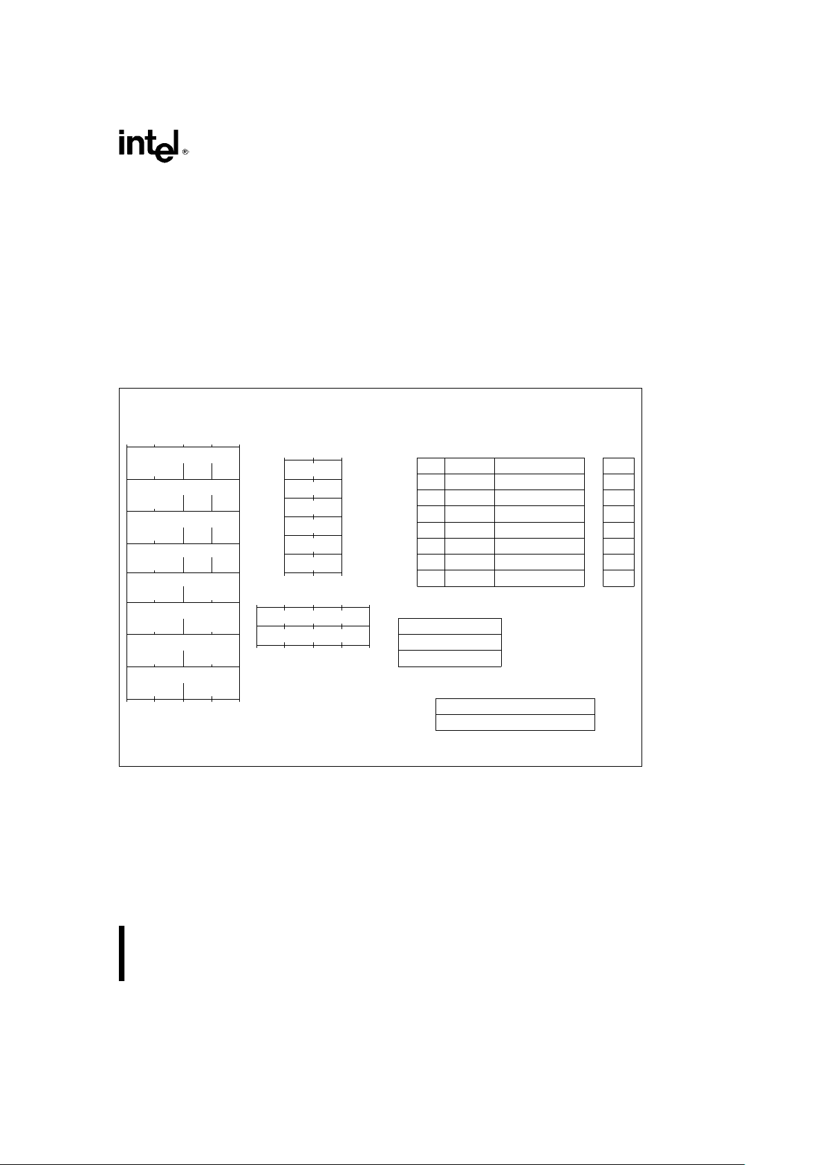
Figure 3-1 shows the Intel387 SX Math CoProcessor
register set. When a Math CoProcessor is present in
a system, programmers may use these registers in
addition to the registers normally available on the
CPU.
i386TMMicroprocessor Registers i387TMMath CoProcessor Data Registers
GENERAL REGISTERS
31 16 15 0
EAX
AX
AH AL
EBX
BX
BH BL
ECX
CX
CH CL
EDX
DX
DH DL
ESI SI
EDI DI
EBP BP
ESP SP
SEGMENT REGISTERS
15 0
CS
SS
DS
ES
FS
GS
31 0
EIP
EFLAGS
Tag
Field
79 78 64 63 0 1 0
R0 Sign Exponent Significand
R1
R2
R3
R4
R5
R6
R7
15 0
Control Register
Status Register
Tag Word
47 0
Instruction Pointer (in CPU)
Data Pointer (in CPU)
l
l
l
l
l
l
l
l
l
l
l
l
l
l
l
l
l
l
l
l
l
l
l
l
l
l
l
l
l
l
l
Figure 3-1. Intel386TMCPU and Intel387TMMath CoProcessor Register Set
11
11
Intel387TMSX MATH COPROCESSOR
3.2.1 STATUS WORD (SW) REGISTER
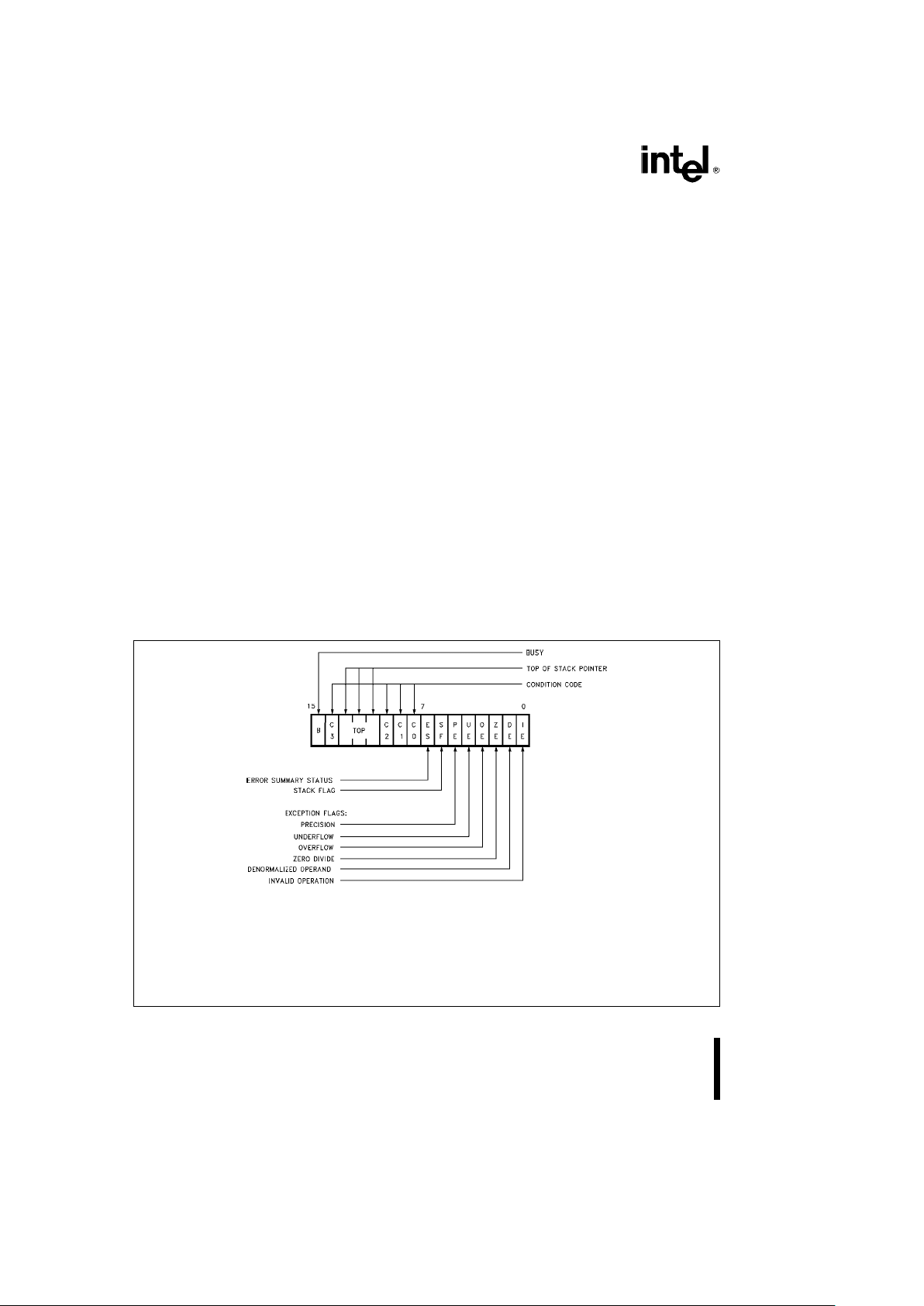
The 16-bit status word (in the status register) shown
in Figure 3-2 reflects the overall state of the Math
CoProcessor. It can be read and inspected by programs using the FSTSW memory or FSTSW AX instructions.
Bit 15, the Busy bit (B) is included for 8087 compatibility only. It always has the same value as the Error
Summary bit (ES, bit 7 of status word); it does not
indicate the status of the BUSY
Ý
output of the Math
CoProcessor.
Bits 13–11 (TOP) serves as the pointer to the Math
CoProcessor data register that is the current Top-OfStack. The significance of the stack top is described
in Section 3.2.5 Data Registers.
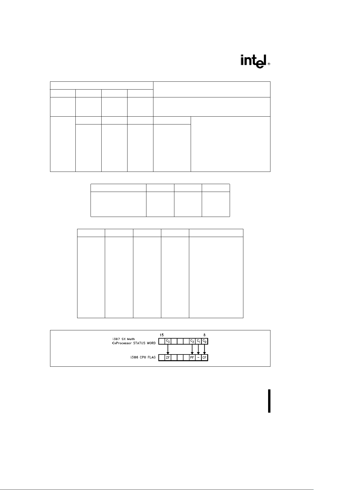
The four numeric condition code bits (C
3–C0
, Bit 14,
10–8) are similar to the flags in a CPU; instructions
that perform arithmetic operations update these bits
to reflect the outcome. The effects of the instructions on the condition code are summarized in Tables 3-1 through 3-4. These condition code bits are
used principally for conditional branching. The
FSTSW AX instructions stores the Math CoProcessor status word directly to the CPU AX register, allowing the condition codes to be inspected efficiently by Intel386 CPU code. The Intel386 CPU SAHF
instruction can copy C
3–C0
directly to the flag bits to
simplify conditional branching. Table 3-5 shows the
mapping of these bits to the Intel386 CPU flag bits.
Bit 7 is the error summary (ES) status bit. This bit is
set if any unmasked exception bit is set; it is clear
otherwise. If this bit is set, the ERROR
Ý
signal is
asserted.
Bit 6 is the stack flag (SF). This bit is used to distinguish invalid operations due to stack overflow or underflow from other kinds of invalid operations. When
SF is set, bit 9 (C
1
) distinguishes between stack
overflow (C
1
e
1) or underflow (C
1
e
0).
Bit 5 – 0 are the six exception flags of the status word
and are set to indicate that during an instruction execution the Math CoProcessor has detected one of
six possible exception conditions since these status
bits were last cleared or reset. Section 3.5 entitled
Exception Handling explains how they are set and
used.
The exception flags are ‘‘sticky’’ bits and can only
be cleared by the instructions FINIT, FCLEX,
FLDENV, FSAVE, and FRSTOR. Note that when a
new value is loaded into the status word by the
FLDENV or FRSTOR instruction, the value of ES (bit
7) and B (bit 15) are not derived from the values
loaded from memory but rather are dependent upon
the values of the exception flags (bits 5 – 0) in the
status word and their corresponding masks in the
control word. If ES is set in such a case, the
ERROR
Ý
output of the Math CoProcessor is acti-
vated immediately.
240225– 3
ES is set if any unmasked exception bit is set; cleared otherwise. See Table 2-2 for interpretation of condition code.
TOP values:
000
e
Register 0 is Top of Stack
001
e
Register 1 is Top of Stack
.
.
.
111
e
Register 7 is Top of Stack
For definitions of exceptions, refer to the section entitled ‘‘Exception Handling’’
Figure 3-2. Status Word
12
12

Intel387TMSX MATH COPROCESSOR
Table 3-1. Condition Code Interpretation
Instruction C0 (S) C3 (Z) C1 (A) C2 (C)
FPREM, FPREM1 Three least significant bits
Reduction
(see Table 3-2) of quotient
0
e
complete
Q2 Q0 Q1
1
e
incomplete
or O/U
Ý
FCOM, FCOMP,
FCOMPP, FTST, Result of comparison
Zero
Operand is not
FUCOM, FUCOMP, (see Table 3-3)
or O/U
Ý
comparable
FUCOMPP, FICOM, (Table 3-3)
FICOMP
FXAM Operand class Sign Operand class
(see Table 3-4) or O/U
Ý
(Table 3-4)
FCHS, FABS, FXCH,
FINCSTP, FDECSTP,
Zero
Constant loads, UNDEFINED UNDEFINED
FXTRACT, FLD,
or O/U
Ý
FILD, FBLD,
FSTP (ext real)
FIST, FBSTP,
FRNDINT, FST,
FSTP, FADD, FMUL,
Roundup
FDIV, FDIVR, UNDEFINED UNDEFINED
FSUB, FSUBR,
or O/U
Ý
FSCALE, FSQRT,
FPATAN, F2XM1,
FYL2X, FYL2XP1
FPTAN, FSIN Roundup Reduction
FCOS, FSINCOS UNDEFINED or O/U
Ý
,0
e
complete
undefined 1
e
incomplete
if C2
e
1
FLDENV, FRSTOR Each bit loaded from memory
FLDCW, FSTENV,
FSTCW, FSTSW, UNDEFINED
FCLEX, FINIT,
FSAVE
O/U
Ý
When both IE and SF bits of status word are set, indicating a stack exception, this bit
distinguishes between stack overflow (C1
e
1) and underflow (C1e0).
Reduction If FPREM or FPREM1 produces a remainder that is less than the modulus, reduction is
complete. When reduction is incomplete the value at the top of the stack is a partial
remainder, which can be used as input to further reduction. For FPTAN, FSIN, FCOS, and
FSINCOS, the reduction bit is set if the operand at the top of the stack is too large. In this
case the original operand remains at the top of the stack.
Roundup When the PE bit of the status word is set, this bit indicates whether the last rounding in the
instruction was upward.
UNDEFINED Do not rely on finding any specific value in these bits.
13
13
Intel387TMSX MATH COPROCESSOR
Table 3-2. Condition Code Interpretation after FPREM and FPREM1 Instructions
Condition Code
Interpretation after FPREM and FPREM1
C2 C3 C1 C0
Incomplete Reduction:
1 X X X further interation required
for complete reduction
Q1 Q0 Q2 Q MOD8
000 0
010 1
Complete Reduction:
0
100 2
C0, C3, C1 contain three least
110 3
significant bits of quotient
001 4
011 5
101 6
111 7
Table 3-3. Condition Code Resulting from Comparison
Order C3 C2 C0
TOPlOperand 0 0 0
TOP
k
Operand 0 0 1
TOP
e
Operand 1 0 0
Unordered 1 1 1
Table 3-4. Condition Code Defining Operand Class
C3 C2 C1 C0 Value at TOP
0000
a
Unsupported
0001
a
NaN
0010
b
Unsupported
0011
b
NaN
0100
a
Normal
0101
a
Infinity
0110
b
Normal
0111
b
Infinity
1000
a
0
1001
a
Empty
1010
b
0
1011
b
Empty
1100
a
Denormal
1110
b
Denormal
Table 3-5 Mapping Condition Codes to Intel386TMCPU Flag Bits
240225– 4
14
14
Intel387TMSX MATH COPROCESSOR
3.2.2 CONTROL WORD (CW) REGISTER
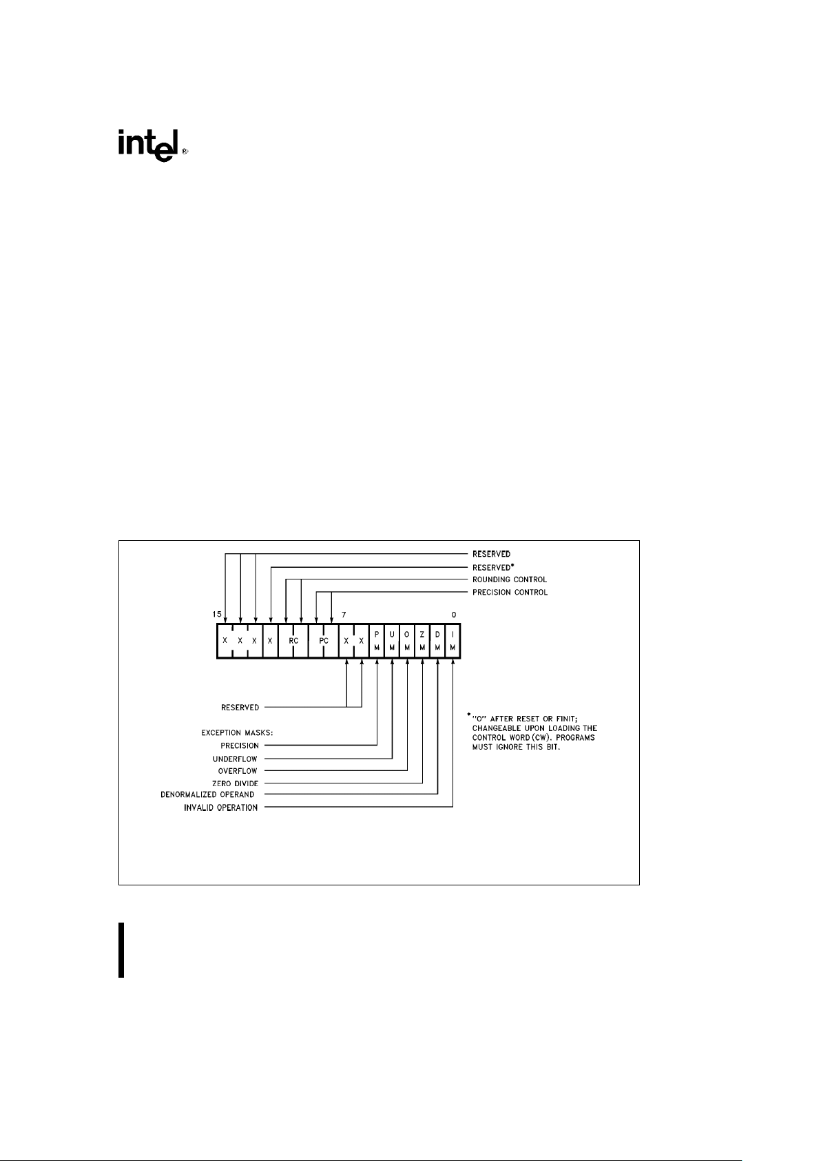
The Math CoProcessor provides the programmer
with several processing options that are selected by
loading a control word from memory into the control
register. Figure 3-3 show the format and encoding of
fields in the control word.
The low-order byte of the control word register is
used to configure the exception masking. Bits 5–0
of the control word contain individual masks for each
of the six exceptions that the Math CoProcessor recognizes. See Section 3.5, Exception Handling, for
further explanation on the exception control and definition.
The high-order byte of the control word is used to
configure the Math CoProcessor operating mode, including precision, rounding and infinity control.
#
The rounding control (RC) field (bits 11 – 10) provide for directed rounding and true chop, as well
as the unbiased round to nearest even mode
specified in the IEEE standard. Rounding control
affects only those instructions that perform
rounding at the end of the operation (and thus
can generate a precision exception); namely,
FST, FSTP, FIST, all arithmetic instructions (except FPREM, FPREM1, FXTRACT, FABS, and
FCHS) and all transcendental instructions.
#
The precision control (PC) field (bits 9–8) can be
used to set the Math CoProcessor internal operating precision of the significand at less than the
default of 64 bits (extended precision). This can
be useful in providing compatibility with early generation arithmetic processors of smaller precision. PC affects only the instructions FADD,
FSUB(R), FMUL, FDIV(R), and FSQRT. For all
other instructions, either the precision is determined by the opcode or extended precision is
used.
#
The ‘‘infinity control bit’’ (bit 12) is not meaningful
to the Intel387 SX Math CoProcessor and programs must ignore its value. To maintain compatibility with the 8087 and 80287 (non-387 core),
this bit can be programmed, however, regardless
of its value the Intel387 SX Math CoProcessor
always treats infinity in the affine sense (
b%
k
a %
). This bit is initialized to zero both after a
hardware reset and after FINIT instruction.
All other bits are reserved and should not be programmed, to assure compatibility with future processors.
240225– 5
Precision Control
00Ð24 bits (single precision)
01Ð(reserved)
10Ð53 bits (double precision)
11Ð64 bits (extended precision)
Rounding Control
00ÐRound to nearest or even
01ÐRound down (toward
b%
)
10ÐRound up (toward
a %
)
11ÐChop (truncate toward zero)
Figure 3-3. Control Word
15
15
 Loading...