


January 1994 Order Number: 271114-004
M87C51FC
CHMOS SINGLE-CHIP 8-BIT MICROCONTROLLER
WITH 32 KBYTES USER PROGRAMMABLE EPROM
Military
M87C51FCÐ3.5 MHz to 12 MHz, V
CC
e
5Vg20%
M87C51FC-1Ð3.5 MHz to 16 MHz, V
CC
e
5Vg20%
Y
High Performance CHMOS EPROM
Y
Three 16-Bit Timer/Counters
Y
Programmable Clock Out
Y
Programmable Counter Array with:
Ð High Speed Output,
Ð Compare/Capture,
Ð Pulse Width Modulator,
Ð Watchdog Timer Capabilities
Y
Up/Down Timer/Counter
Y
Three Level Program Lock System
Y
32K On-Chip EPROM
Y
256 Bytes of On-Chip Data RAM
Y
Improved Quick Pulse Programming
Algorithm
Y
Boolean Processor
Y
Available in 40-pin Cerdip and 44-pin
LCC Packages
Y
32 Programmable I/O Lines
Y
7 Interrupt Sources
Y
Programmable Serial Channel with:
Ð Framing Error Detection
Ð Automatic Address Recognition
Y
TTL and CMOS Compatible Logic
Levels
Y
64K External Program Memory Space
Y
64K External Data Memory Space
Y
MCSÉ-51 Fully Compatible Instruction
Set
Y
Power Saving Idle and Power Down
Modes
Y
ONCE (On-Circuit Emulation) Mode
Y
Available in Two Product Grades:
Ð MIL-STD-883,
b
55§Ctoa125§C(TC)
Ð Military Temperature Only (MTO)
b
55§Ctoa125§C(TC)
MEMORY ORGANIZATION
PROGRAM MEMORY: Up to 32 Kbytes of the program memory can reside in the on-chip EPROM. In addition
the device can address up to 64K of program memory external to the chip.
DATA MEMORY: This microcontroller has a 256 x 8 on-chip RAM. In addition it can address up to 64 Kbytes of
external data memory.
The Intel M87C51FC is a single-chip control-oriented microcontroller which is fabricated on Intel’s reliable
CHMOS III-E technology. Being a member of the MCS-51 family, the M87C51FC uses the same powerful
instruction set, has the same architecture, and is pin-for-pin compatible with the existing MCS-51 family of
products. The M87C51FC is an enhanced version of the 87C51. Its added features make it an even more
powerful microcontroller for applications that require Pulse Width Modulation, High Speed I/O, and up/down
counting capabilities such as motor control. It also has a more versatile serial channel that facilitates multiprocessor communications.

M87C51FC
271114–1
Figure 1. M87C51FC Block Diagram
2
M87C51FC
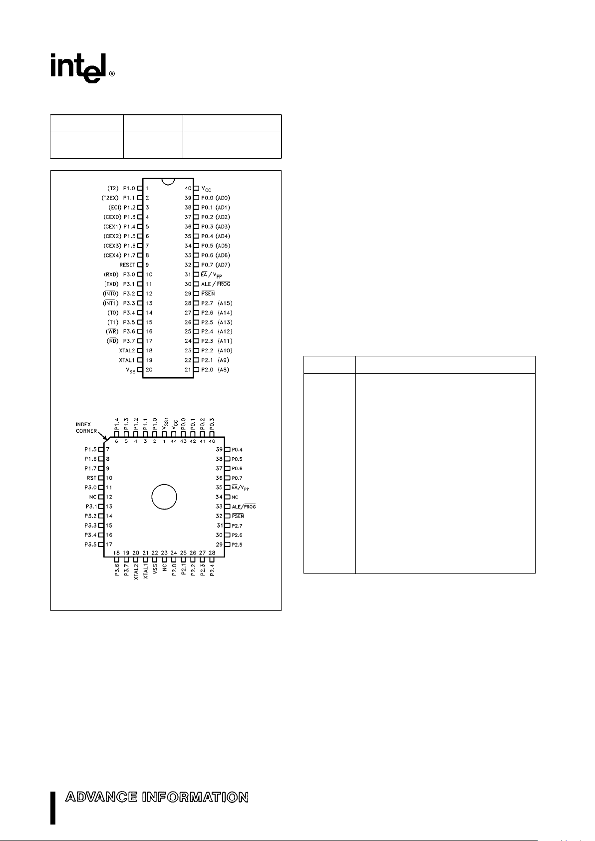
PACKAGES
Part Prefix Package Type
87C51FC D 40-Pin CERDIP
R 44-Pin LCC
271114–2
DIP
271114–3
LCC
Figure 2. Pin Connections
PIN DESCRIPTIONS
VCC: Supply voltage.
VSS: Circuit ground.
Port 0: Port 0 is an 8-bit, open drain, bidirectional I/O
port. As an output port each pin can sink several LS
TTL inputs. Port 0 pins that have 1’s written to them
float, and in that state can be used as high-impedance inputs.
Port 0 is also the multiplexed low-order address and
data bus during accesses to external Program and
Data Memory. In this application it uses strong internal pullups when emitting1’s, and can source and
sink several LS TTL inputs.
Port 0 also receives the code bytes during EPROM
programming, and outputs the code bytes during
program verification. External pullup resistors are required during program verification.
Port 1: Port 1 is an 8-bit bidirectional I/O port with
internal pullups. The Port 1 output buffers can drive
LS TTL inputs. Port 1 pins that have 1’s written to
them are pulled high by the internal pullups, and in
that state can be used as inputs. As inputs, Port 1
pins that are externally being pulled low will source
current (I
IL
, on the data sheet) because of the inter-
nal pullups.
In addition, Port 1 serves the functions of the following special features of the M87C51FC:
Port Pin Alternate Function
P1.0 T2 (External Count Input to Timer/
Counter 2), Clock-Out
P1.1 T2EX (Timer/Counter 2 Capture/
Reload Trigger and Direction Control)
P1.2 ECI (External Count Input to the PCA)
P1.3 CEX0 (External I/O for Compare/
Capture Module 0)
P1.4 CEX1 (External I/O for Compare/
Capture Module 1)
P1.5 CEX2 (External I/O for Compare/
Capture Module 2)
P1.6 CEX3 (External I/O for Compare/
Capture Module 3)
P1.7 CEX4 (External I/O for Compare/
Capture Module 4)
Port 1 receives the low-order address bytes during
EPROM programming and verifying.
Port 2: Port 2 is an 8-bit bidirectional I/O port with
internal pullups. The Port 2 output buffers can drive
LS TTL inputs. Port 2 pins that have 1’s written to
them are pulled high by the internal pullups, and in
that state can be used as inputs. As inputs, Port 2
pins that are externally being pulled low will source
current (I
IL
, on the data sheet) because of the inter-
nal pullups.
3
M87C51FC
Port 2 emits the high-order address byte during
fetches from external Program Memory and during
accesses to external Data Memory that use 16-bit
addresses (MOVX
@
DPTR). In this application it
uses strong internal pullups when emitting 1’s. During accesses to external Data Memory that use 8-bit
addresses (MOVX
@
Ri), Port 2 emits the contents of
the P2 Special Function Register.
Some Port 2 pins receive the high-order address bits
during EPROM programming and program verification.
Port 3: Port 3 is an 8-bit bidirectional I/O port with
internal pullups. The Port 3 output buffers can drive
LS TTL inputs. Port 3 pins that have 1’s written to
them are pulled high by the internal pullups, and in
that state can be used as inputs. As inputs, Port 3
pins that are externally being pulled low will source
current (I
IL
, on the data sheet) because of the pull-
ups.
Port 3 also serves the functions of various special
features of the MCS-51 Family, as listed below:
Port Pin Alternate Function
P3.0 RXD (serial input port)
P3.1 TXD (serial output port)
P3.2 INT0
(external interrupt 0)
P3.3 INT1
(external interrupt 1)
P3.4 T0 (Timer 0 external input)
P3.5 T1 (Timer 1 external input)
P3.6 WR (external data memory write strobe)
P3.7 RD
(external data memory read strobe)
Some Port 3 pins receive the high-order address bits
during EPROM programming and program verification.
RST: Reset input. A high on this pin for two machine
cycles while the oscillator is running resets the device. An internal pulldown resistor permits a poweron reset with only a capacitor connected to V
CC
.
ALE: Address Latch Enable output pulse for latching
the low byte of the address during accesses to external memory. This pin (ALE/PROG
) is also the
program pulse input during EPROM programming for
the M87C51FC.
In normal operation ALE is emitted at a constant
rate of (/6 the oscillator frequency, and may be used
for external timing or clocking purposes. Note, however, that one ALE pulse is skipped during each access to external Data Memory.
Throughout the remainder of this data sheet, ALE
will refer to the signal coming out of the ALE/PROG
pin, and the pin will be referred to as the ALE/PROG
pin.
PSEN
: Program Store Enable is the read strobe to
external Program Memory.
When the M87C51FC is executing code from external Program Memory, PSEN
is activated twice each
machine cycle, except that two PSEN
activations
are skipped during each access to external Data
Memory.
EA
/VPP: External Access enable. EA must be
strapped to VSS in order to enable the device to
fetch code from external Program Memory locations
0000H to 0FFFFH. Note, however, that if either of
the Program Lock bits are programmed, EA
will be
internally latched on reset.
EA should be strapped to VCCfor internal program
executions.
This pin also receives the programming supply voltage (V
PP
) during EPROM programming.
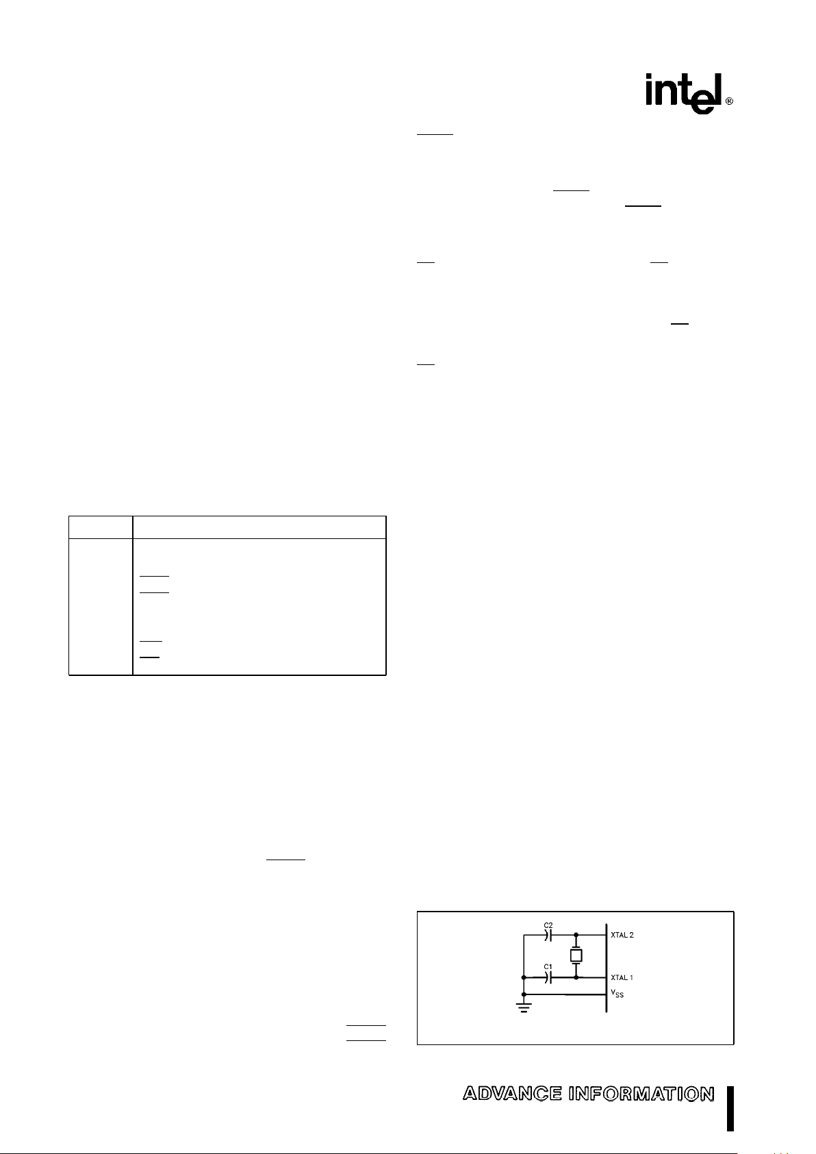
XTAL1: Input to the inverting oscillator amplifier.
XTAL2: Output from the inverting oscillator amplifier.
OSCILLATOR CHARACTERISTICS
XTAL1 and XTAL2 are the input and output, respectively, of a inverting amplifier which can be configured for use as an on-chip oscillator, as shown in
Figure 3. Either a quartz crystal or ceramic resonator
may be used. More detailed information concerning
the use of the on-chip oscillator is available in Application Note AP-155, ‘‘Oscillators for Microcontrollers.’’
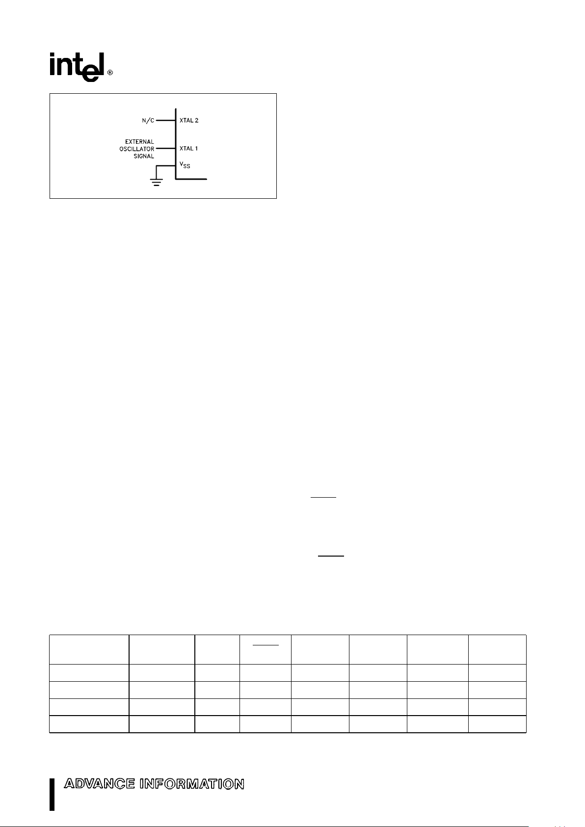
To drive the device from an external clock source,
XTAL1 should be driven, while XTAL2 floats, as
shown in Figure 4. There are no requirements on the
duty cycle of the external clock signal, since the input to the internal clocking circuitry is through a divide-by-two flip-flop, but minimum and maximum
high and low times specified on the data sheet must
be observed.
An external oscillator may encounter as much as a
100 pF load at XTAL1 when it starts up. This is due
to interaction between the amplifier and its feedback
capacitance. Once the external signal meets the V
IL
and VIHspecifications the capacitance will not exceed 20 pF.
271114–4
C1, C2
e
30 pFg10 pF for Crystals
e
10 pF for Ceramic Resonators
Figure 3. Oscillator Connections
4
M87C51FC
271114–5
Figure 4. External Clock Drive Configuration
IDLE MODE
The user’s software can invoke the Idle Mode. When
the microcontroller is in this mode, power consumption is reduced. The Special Function Registers and
the onboard RAM retain their values during Idle, but
the processor stops executing instructions. Idle
Mode will be exited if the chip is reset or if an enabled interrupt occurs. The PCA timer/counter can
optionally be left running or paused during Idle
Mode.
POWER DOWN MODE
To save even more power, a Power Down mode can
be invoked by software. In this mode, the oscillator
is stopped and the instruction that invoked Power
Down is the last instruction executed. The on-chip
RAM and Special Function Registers retain their values until the Power Down mode is terminated.
On the M87C51FC either a hardware reset or an
external interrupt can cause an exit from Power
Down. Reset redefines all the SFRs but does not
change the on-chip RAM. An external interrupt allows both the SFRs and on-chip RAM to retain their
values.
To properly terminate Power down the reset or external interrupt should not be executed before V
CC
is
restored to its normal operating level and must be
held active long enough for the oscillator to restart
and stabilize (normally less than 10 ms).
With an external interrupt, INT0 and INT1 must be
enabled and configured as level-sensitive. Holding
the pin low restarts the oscillator but bringing the pin
back high completes the exit. Once the interrupt is
serviced, the next instruction to be executed after
RETI will be the one following the instruction that put
the device into Power Down.
DESIGN CONSIDERATION
#
The window on the M87C51FC must be covered
by an opaque label. Otherwise, the DC and AC
characteristics may not be met, and the device
may functionally be impaired.
#
When the idle mode is terminated by a hardware
reset, the device normally resumes program execution, from where it left off, up to two machine
cycles before the internal reset algorithm takes
control. On-chip hardware inhibits access to internal RAM in this event, but access to the port pins
is not inhibited. To eliminate the possibility of an
unexpected write when Idle is terminated by reset, the instruction following the one that invokes
Idle should not be one that writes to a port pin or
to external memory.
ONCE MODE
The ONCE (‘‘On-Circuit Emulation’’) Mode facilitates
testing and debugging of systems using the
M87C51FC without the M87C51FC having to be removed from the circuit. The ONCE Mode is invoked
by:
1) Pull ALE low while the device is in reset and
PSEN
is high;
2) Hold ALE low as RST is deactivated.
While the device is in ONCE Mode, the Port 0 pins
go into a float state, and the other port pins and ALE
and PSEN
are weakly pulled high. The oscillator circuit remains active. While the M87C51FC is in this
mode, an emulator or test CPU can be used to drive
the circuit. Normal operation is restored when a normal reset is applied.
Table 1. Status of the External Pins during Idle and Power Down
Mode
Program
ALE PSEN PORT0 PORT1 PORT2 PORT3
Memory
Idle Internal 1 1 Data Data Data Data
Idle External 1 1 Float Data Address Data
Power Down Internal 0 0 Data Data Data Data
Power Down External 0 0 Float Data Data Data
NOTE:
For more detailed information on the reduced power modes refer to Application Note AP-255, ‘‘Military CHMOS: Designing
with the M80C51BH.’’
5

M87C51FC
ABSOLUTE MAXIMUM RATINGS*
Case Temperature Under BiasÀÀÀb55§Ctoa125§C
Storage Temperature ААААААААААb65§Ctoa150§C
Voltage on EA/V
PP
Pin to VSSААААААА0V toa13.0V
Voltage on Any Other Pin to VSSÀÀb0.5V toa6.5V
IOLPer I/O Pin ААААААААААААААААААААААААААА15 mA
Power DissipationАААААААААААААААААААААААААА1.5W
(based on PACKAGE heat transfer limitations, not
device power consumption)
NOTICE: This data sheet contains information on
products in the sampling and initial production phases
of development. The specifications are subject to
change without notice. Verify with your local Intel
Sales office that you have the latest data sheet before finalizing a design.
*
WARNING: Stressing the device beyond the ‘‘Absolute
Maximum Ratings’’ may cause permanent damage.
These are stress ratings only. Operation beyond the
‘‘Operating Conditions’’ is not recommended and extended exposure beyond the ‘‘Operating Conditions’’
may affect device reliability.
ADVANCED INFORMATIONÐCONTACT INTEL FOR DESIGN-IN INFORMATION
OPERATING CONDITIONS
MIL-STD-883
Symbol Parameter Min Max Units
T
C
Case Temperature (Instant On)
b
55
a
125
§
C
V
CC
Digital Supply Voltage 4.00 6.00 V
f
OSC
Oscillator Frequency 3.5 16 MHz
Military Temperature (MTO)
Symbol Parameter Min Max Units
T
C
Case Temperature (Instant On)
b
55
a
125
§
C
V
CC
Digital Supply Voltage 4.00 6.00 V
f
OSC
Oscillator Frequency 3.5 16 MHz
DC CHARACTERISTICS (Over Specified Operating Conditions)
Symbol Parameter Min Max Unit Comments
V
IL
Input Low Voltage
b
0.5 0.2 V
CC
b
0.1 V
V
IH
Input High Voltage 0.2 V
CC
a
0.9 V
CC
a
0.5 V
(Except XTAL1, RST)
V
IH1
Input High Voltage 0.7 V
CC
V
CC
a
0.5 V
(XTAL1, RST)
V
OL
Output Low Voltage (Note 4) 0.3 V I
OL
e
100 mA (Note 1)
(Ports 1, 2, and 3)
0.45 V I
OL
e
1.6 mA (Note 1)
1.0 V I
OL
e
3.5 mA (Note 1)
V
OL1
Output Low Voltage (Note 4) 0.3 V I
OL
e
200 mA (Note 1)
(Port 0, ALE, PSEN)
0.45 V I
OL
e
3.2 mA (Note 1)
1.0 V I
OL
e
7.0 mA (Note 1)
V
OH
Output High Voltage V
CC
b
0.3 V I
OH
eb
10 mA
(Ports 1, 2, and 3, ALE, PSEN)
V
CC
b
0.7 V I
OH
eb
30 mA
V
CC
b
1.5 V I
OH
eb
60 mA
6

M87C51FC
DC CHARACTERISTICS (Over Specified Operating Conditions) (Continued)
Symbol Parameter Min Max Unit Comments
V
OH1
Output High Voltage V
CC
b
0.3 V I
OH
eb
200 mA
(Port 0 in External Bus Mode)
V
CC
b
0.7 V I
OH
eb
3.2 mA
V
CC
b
1.5 V I
OH
eb
7.0 mA
I
IL
Logical 0 Input Current
b
75 mAV
IN
e
0.45V
(Ports 1, 2, and 3)
I
LI
Input leakage Current (Port 0)
g
10 mA0
k
V
IN
k
V
CC
I
TL
Logical 1 to 0 Transition
b
750 mAV
IN
e
2V
Current (Ports 1, 2, and 3)
RRST RST Pulldown Resistor 40 225 KX
CIO Pin Capacitance 10 pF
@
1 MHz, 25§C
I
CC
Power Supply Current: (Note 3)
Running at 12 MHz (Figure 6) 40 mA
Idle Mode at 12 MHz (Figure 7) 10 mA
Power Down Mode (Figure 8) 100 mA
Running at 16 MHz 45 mA
Idle Mode at 16 MHz 15 mA
Power Down Mode 16 MHz 130 mA
NOTES:
1. Capacitive loading on Ports 0 and 2 may cause spurious noise pulses to be superimposed on the VOLs of ALE and Ports
1, 2 and 3. The noise is due to external bus capacitance discharging into the Port 0 and Port 2 pins when these pins make 1
to 0 transitions during bus operations. In applications where capacitance loading exceeds 100 pFs, the noise pulse on the
ALE signal may exceed 0.8V. In these cases, it may be desirable to qualify ALE with a Schmitt Trigger, or use an Address
Latch with a Schmitt Trigger Strobe input.
2. Capacitive loading on Ports 0 and 2 cause the V
OH
on ALE and PSEN to drop below the 0.9 VCCspecification when the
address lines are stabilizing.
3. See Figures 6 – 9 for load circuits. Minimum V
CC
for Power Down is 2V.
4. Under steady state (non-transient) conditions, IOLmust be externally limited as follows:
Maximum IOLper port pin: 10mA
Maximum IOLper 8-bit portÐ
Port 0: 26 mA
Ports 1, 2 and 3: 15 mA
Maximum total IOLfor all output pins: 71 mA
If I
OL
exceeds the test condition, VOLmay exceed the related specification. Pins are not guaranteed to sink current greater
than the listed test conditions.
271114–6
I
CC
Max at other frequencies is given by:
Active Mode
I
CC
Maxe(Osc Freqc3)a4
Idle Mode
I
CC
Maxe(Osc Freqc0.5)a4
Where Osc Freq is in MHz, I
CC
is in mA.
Figure 5. ICCvs Frequency
271114–7
All other pins disconnected
TCLCH
e
TCHCLe5ns
Figure 6. ICCLoad Circuits,
Active Mode
7

M87C51FC
271114–8
All other pins disconnected
TCLCH
e
TCHCLe5ns
Figure 7. ICCLoad Circuit Idle Mode
271114–9
All other pins disconnected
Figure 8. ICCLoad Circuit, Power Down Mode.
V
CC
e
2.0V to 5.5V.
271114–10
Figure 9. Clock Signal Waveform for ICCTests in Active and Idle Modes. TCLCHeTCHCLe5 ns.
EXPLANATION OF THE AC SYMBOLS
Each timing symbol has 5 characters. The first character is always a ‘T’ (stands for time). The other
characters, depending on their positions, stand for
the name of a signal or the logical status of that
signal. The following is a list of all the characters and
what they stand for.
A: Address
C: Clock
D: Input Data
H: Logic level HIGH
I: Instruction (program memory contents)
L: Logic level LOW, or ALE
P: PSEN
Q: Output Data
R: RD
signal
T: Time
V: Valid
W: WR
signal
X: No longer a valid logic level
Z: Float
For example,
TAVLL
e
Time from Address Valid to ALE Low
TLLPL
e
Time from ALE Low to PSEN Low
8

M87C51FC
AC CHARACTERISTICS (Over Specified Operating Conditions, Load Capacitance for Port 0,
ALE/PROG
and PSENe100 pF, Load Capacitance for All Other Outputse80 pF)
ADVANCED INFORMATIONÐCONTACT INTEL FOR DESIGN-IN INFORMATION
EXTERNAL PROGRAM MEMORY CHARACTERISTICS
Symbol Parameter
12 MHz 16 MHz Variable
Units
Oscillator Oscillator Oscillator
Min Max Min Max Min Max
1/TCLCL Oscillator Frequency 3.5 16 MHz
TLHLL ALE Pulse Width 127 85 2TCLCLb40 ns
TAVLL Address Valid to ALE Low 43 23 TCLCLb40 ns
TLLAX Address Hold 53 33 TCLCLb30 ns
After ALE Low
TLLIV ALE Low to 234 150 4TCLCLb100 ns
Valid Instruction In
TLLPL ALE Low to PSEN Low 53 33 TCLCLb30 ns
TPLPH PSEN Pulse Width 205 143 3TCLCLb45 ns
TPLIV PSEN Low to 145 83 3TCLCLb105 ns
Valid Instruction In
TPXIX Input Instruction Hold 0 0 0 ns
After PSEN
TPXIZ Input Instruction Float 59 38 TCLCLb25 ns
Float After PSEN
TAVIV Address to 312 208 5TCLCLb105 ns
Valid Instruction In
TPLAZ PSEN Low to 10 10 10 ns
Address Float
TRLRH RD Pulse Width 400 275 6TCLCLb100 ns
TWLWH WR Pulse Width 400 275 6TCLCLb100 ns
TRLDV RD Low to Valid Data In 252 147.5 5TCLCLb165 ns
TRHDX Data Hold After RD 00 0 ns
TRHDZ Data Float After RD 107 65 2TCLCLb60 ns
TLLDV ALE Low to Valid Data In 517 350 8TCLCLb150 ns
TAVDV Address to Valid Data In 585 398 9TCLCLb165 ns
TLLWL ALE Low to 200 300 138 238 3TCLCLb50 3TCLCLa50 ns
RD
or WR Low
TAVWL Address Valid to WR Low 203 120 4TCLCLb130 ns
TQVWX Data Valid before WR 33 13 TCLCLb50 ns
TWHQX Data Hold after WR 33 13 TCLCLb50 ns
TQVWH Data Valid to WR High 433 288 7TCLCLb150 ns
TRLAZ RD Low to 0 0 0 ns
Address Float
TWHLH RD or WR High 43 123 23 103 TCLCLb40 TCLCLa40 ns
to ALE High
9

M87C51FC
EXTERNAL PROGRAM MEMORY READ CYCLE
271114–11
EXTERNAL DATA MEMORY READ CYCLE
271114–12
EXTERNAL DATA MEMORY WRITE CYCLE
271114–13
10

M87C51FC
SERIAL PORT TIMING - SHIFT REGISTER MODE
Test Conditions:
T
C
eb
55§Ctoa125§C; V
CC
e
5Vg10%; V
SS
e
0V; Load Capacitancee80 pF
Symbol Parameter
12 MHz 16 MHz Variable
Units
Oscillator Oscillator Oscillator
Min Max Min Max Min Max
TXLXL Serial Port Clock 1 0.75 12TCLCL ms
Cycle Time
TQVXH Output Data Setup to 700 492 10TCLCLb133 ns
Clock Rising Edge
TXHQX Output Data Hold After 50 8 2TCLCLb117 ns
Clock Rising Edge
TXHDX Input Data Hold After 0 0 0 ns
Clock Rising Edge
TXHDV Clock Rising Edge to 700 492 10TCLCLb133 ns
Input Data Valid
SHIFT REGISTER MODE TIMING WAVEFORMS
271114–14
EXTERNAL CLOCK DRIVE
Symbol Parameter Min Max Units
1/TCLCL Oscillator Frequency
M87C51FC 3.5 12
MHz
M87C51FC-16 3.5 16
TCHCX High Time 20 ns
TCLCX Low Time 20 ns
TCLCH Rise Time 20 ns
TCHCL Fall Time 20 ns
EXTERNAL CLOCK DRIVE WAVEFORM
271114–15
11

M87C51FC
AC TESTING INPUT, OUTPUT WAVEFORMS
271114–16
AC Inputs during testing are driven at V
CC
b
0.5V for a Logic ‘‘1’’
and 0.45V for a Logic ‘‘0’’. Timing measurements are made at V
IH
min for a Logic ‘‘1’’ and VILmax for a Logic ‘‘0’’.
FLOAT WAVEFORMS
271114–17
For timing purposes a port pin is no longer floating when a
100 mV change from load voltage occurs, and begins to float
when a 100 mV change from the loaded V
OH/VOL
level occurs.
I
OL/IOH
t
g
20 mA.
Table 2. EPROM Programming Modes
Mode RST PSEN
ALE/ EA/
P2.6 P2.7 P3.3 P3.6 P3.7
PROG
V
PP
Program Code Data H L ß 12.75V L H H H H
Verify Code Data H L H H L L L H H
Program Encryption H L ß 12.75V L H H L H
Array Address 0 – 3FH
Program Lock Bit 1 H L ß 12.75V H H H H H
Bits
Bit 2 H L ß 12.75V H H H L L
Bit 3 H L ß 12.75V H L H H L
Read Signature Byte H L H H L L L L L
DEFINITION OF TERMS
ADDRESS LINES: P1.0– P1.7, P2.0 –P2.5, P3.4 –
P3.5 respectively for A0– A15.
DATA LINES: P0.0 – P0.7 for D0– D7.
CONTROL SIGNALS: RST, PSEN
, P2.6, P2.7, P3.3,
P3.6, P3.7
PROGRAM SIGNALS: ALE/PROG
,EA/V
PP
PROGRAMMING THE EPR OM
The part must be running with a 4 MHz to 6 MHz
oscillator. The address of an EPROM location to be
programmed is applied to address lines while the
code byte to be programmed in that location is applied to data lines. Control and program signals must
be held at the levels indicated in Table 2. Normally
EA
/VPPis held at logic high until just before ALE/
PROG
is to be pulsed. The EA/VPPis raised to VPP,
ALE/PROG
is pulsed low and then EA/VPPis re-
turned to a high (also refer to timing diagrams).
NOTE:
Exceeding the VPPmaximum for any amount of
time could damage the device permanently. The
V
PP
source must be well regulated and free of
glitches.
12

M87C51FC
271114–18
*See Table 2 for proper input on these pins
Figure 10. Programming the EPROM
PROGRAMMING ALGORITHM
Refer to Table 2 and Figures 10 and 11 for address,
data, and control signals set up. To program the
M87C51FC the following sequence must be exercised.
1. Input the valid address on the address lines.
2. Input the appropriate data byte on the data
lines.
3. Activate the correct combination of control signals.
4. Raise EA
/VPPfrom VCCto 12.75Vg0.25V.
5. Pulse ALE/PROG 5 times for the EPROM array, and 25 times for the encryption table and
the lock bits.
Repeat 1 through 5 changing the address and data
for the entire array or until the end of the object file is
reached.
PROGRAM VERIFY
Program verify may be done after each byte that is
programmed, or after a block of bytes that is programmed. In either case a complete verify of the
entire array that has been programmed will ensure a
reliable programming of the M87C51FC.
The lock bits cannot be directly verified. Verification
of the lock bits is done by observing that their features are enabled. Refer to the EPROM Program
Lock section in this data sheet.
271114–19
5 Pulses
Figure 11. Programming Signal’s Waveforms
13

M87C51FC
EPROM Program Lock
The M87C51FC has a 3-bit program lock system
and a 64-byte encryption array which are designed
to protect the onboard program and data against
software piracy.
Encryption Array
Within the EPROM array are 64 bytes of Encryption
Array that are initially unprogrammed (all 1’s). Every
time that a byte is addressed during a verify, 5 address lines are used to select a byte of the Encryption Array. This byte is then exclusive-NOR’ed
(XNOR) with the code byte, creating an Encryption
Verify byte. The algorithm, with the array in the unprogrammed state (all 1’s), will return the code in it’s
original, unmodified form. For programming the Encryption Array, refer to Table 2 (Programming the
EPROM).
Program Lock Bits
The M87C51FC has 3 programmable lock bits that
when programmed according to Table 3 will provide
different levels of protection for the on-chip code
and data.
Erasing the EPROM also erases the encryption array and the program lock bits, returning the part to
full functionality.
Reading the Signature Bytes
The M87C51FC has 3 signature bytes in locations
30H, 31H, and 60H. To read these bytes follow the
procedure for EPROM verify, but activate the control
lines provided in Table 2 for Read Signature Byte.
Location: 30H
e
89H
31He58H
60HeFCH
Erasure Characteristics
Erasure of the EPROM begins to occur when the
chip is exposed to light with wavelength shorter than
approximately 4,000 Angstroms. Since sunlight and
fluorescent lighting have wavelengths in this range,
exposure to these light sources over an extended
time (about 1 week in sunlight, or 3 years in roomlevel fluorescent lighting) could cause inadvertent
erasure. If an application subjects the device to this
type of exposure, it is suggested that an opaque label be placed over the window.
The recommended erasure procedure is exposure
to ultraviolet light (at 2537 Angstroms) to an integrated dose of at least 15 W-sec/cm
2
. Exposing the
EPROM to an ultraviolet lamp of 12,000 mW/cm
2
rating for 30 minutes, at a distance of about 1 inch,
should be sufficient.
Erasure leaves all the EPROM Cells in a 1’s state.
Table 3. Program Lock Bits and the Features
Program Lock Bits
Protection Type
LB1 LB2 LB3
1 U U U No Program Lock features enabled. (Code verify will still be encrypted by the
Encryption Array if programmed.)
2 P U U MOVC instructions executed from external program memory are disabled
from fetching code bytes from internal memory, EA is sampled and latched on
Reset, and further programming of the EPROM is disabled.
3 P P U Same as 2, also verify is disabled.
4 P P P Same as 3, also external execution is disabled.
Any other combination of the lock bits is not defined.
14

M87C51FC
EPROM PROGRAMMING AND VERIFICATION CHARACTERISTICS
(T
A
e
21§Cto27§C; V
CC
e
5Vg10%; V
SS
e
0V)
ADVANCED INFORMATIONÐCONTACT INTEL FOR DESIGN-IN INFORMATION
Symbol Parameter Min Max Units
V
PP
Programming Supply Voltage 12.5 13.0 V
I
PP
Programming Supply Current 75 mA
1/TCLCL Oscillator Frequency 4 6 MHz
TAVGL Address Setup to PROG Low 48TCLCL
TGHAX Address Hold after PROG 48TCLCL
TDVGL Data Setup to PROG Low 48TCLCL
TGHDX Data Hold after PROG 48TCLCL
TEHSH (Enable) High to V
PP
48TCLCL
TSHGL VPPSetup to PROG Low 10 ms
TGHSL VPPHold after PROG 10 ms
TGLGH PROG Width 90 110 ms
TAVQV Address to Data Valid 48TCLCL
TELQV ENABLE Low to Data Valid 48TCLCL
TEHQZ Data Float after ENABLE 0 48TCLCL
TGHGL PROG High to PROG Low 10 ms
EPROM PROGRAMMING AND VERIFICATION WAVEFORMS
271114–20
15
 Loading...