Intel Corporation MR82510, MDP82510 Datasheet
*Other brands and names are the property of their respective owners.
Information in this document is provided in connection with Intel products. Intel assumes no liability whatsoever, including infringement of any patent or
copyright, for sale and use of Intel products except as provided in Intel’s Terms and Conditions of Sale for such products. Intel retains the right to make
changes to these specifications at any time, without notice. Microcomputer Products may have minor variations to this specification known as errata.
March 1996COPYRIGHT©INTEL CORPORATION, 1996 Order Number: 271072-007
M82510
ASYNCHRONOUS SERIAL CONTROLLER
Military
Y
Asynchronous Operation
Ð 5- to 9-Bit Character Format
Ð Baud Rate DC to 288k
Ð Complete Error Detection
Y
Multiple Sampling Windows
Y
Two, Independent, Four-Byte Transmit
and Receive FIFOs
Ð Programmable Threshold
Y
Two, 16-bit Baud Rate Generators/
Timers
Y
System Clock Options
Ð On-Chip Crystal Oscillator
Ð External Clocks
Y
MCSÉ-51 9-Bit Protocol Support
Y
Control Character Recognition
Y
CHMOS III with Power Down Mode
Y
Interrupts Maskable at Two Levels
Y
Auto Echo and Loopback Modes
Y
Seven I/O Pins, Dedicated and General
Purpose
Y
Available in 28-Lead CERDIP and
28-Pad LCC Packages
Y
Military Temperature Range:
b
55§Ctoa125§C(TC)
The Intel CHMOS M82510 is designed to increase system efficiency in asynchronous environments such as
modems, serial portsÐincluding expanding performance areas: MCS
É
-51 9-bit format and high speed async.
The functional support provided in the M82510 is unparalleledÐ2 baud rate generators/timers provide independent data rates or protocol timeouts; a crystal oscillator and smart modem I/O simplify system logic. New
features, dual FIFOs and Control Character Recognition (CCR), dramatically reduce CPU interrupts and increase software efficiency. The M82510’s software versatility allows emulation of the INS 8250A/16450 for
IBM PC AT* compatibility or a high performance mode, configured by 35 control registers. All interrupts are
maskable at 2 levels. The multi-personality I/O pins are configurable as desired. A DPLL and multiple sampling
of serial data improve data reliability for high speed asynchronous communication. The compact 28-pin
M82510 is fabricated in CHMOS III technology and includes a software powerdown option.
*IBM and PC AT are registered trademarks of IBM Corporation.
271072–1
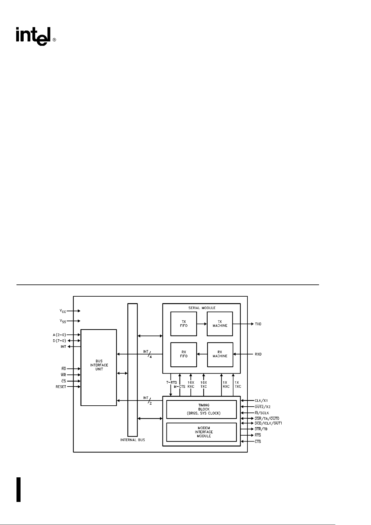
Figure 1. Block Diagram
M82510
28-Pad LCC
271072–55
28-Pin Cerdip
271072–2
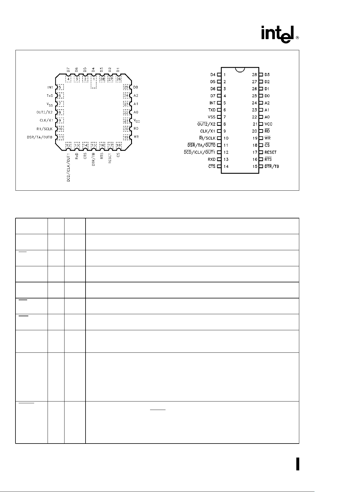
Figure 2. Package Pinouts
M82510 PINOUT DEFINITION
Symbol
Pin
Type Name and Description
No.
RESET 17 I RESET: A high on this input pin resets the M82510 to the Default Wake-up
mode.
CS 18 I CHIP SELECT: A low on this input pin enables the M82510 and allows read or
write operations.
A2– A0 24- I ADDRESS PINS: These inputs interface with three bits of the System Address
22 Bus to select one of the internal registers for read or write.
D7–D0 4* I/O DATA BUS: Bidirectional, three state, eight-bit Data Bus. These pins allow
25 transfer of bytes between the CPU and the M82510.
RD 20 I READ: A low on this input pin allows the CPU to read Data or Status bytes from
the M82510.
WR 19 I WRITE: A low on this input allows the CPU to write Data or Control bytes to the
M82510.
INT 5 O INTERRUPT: A high on this output pin signals an interrupt request to the CPU.
The CPU may determine the particular source and cause of the interrupt by
reading the M82510 Status registers.
CLK/X1 9 I MULTIFUNCTION: This input pin serves as a source for the internal system
clock. The clock may be asynchronous to the serial clocks and to the processor
clock. This pin may be used in one of two modes: CLK Ð in this mode an
externally generated TTL compatible clock should be used to drive this input pin;
X1 Ð in this mode the clock is internally generated by an on-chip crystal
oscillator. This mode requires a crystal to be connected between this pin (X1)
and the X2 pin. (See System Clock Generation.)
OUT2/X2 8 O MULTIFUNCTION: This is a dual function pin which may be configured to one of
the following functions: OUT2
Ð a general purpose output pin controlled by the
CPU, only available when CLK/X1 pin is driven by an externally generated clock;
X2 - this pin serves as an output pin for the crystal oscillator.
Note
: The
configuration of the pin is done only during hardware reset. For more details
refer to the System Clock Generation.
*Pins 28 –25 and Pins 4 – 1.
2
M82510
M82510 PINOUT DEFINITION (Continued)
Symbol
Pin
Type Name and Description
No.
TXD 6 O TRANSMIT DATA: Serial data is transmitted via this output pin starting at the
Least Significant bit.
RXD 13 I RECEIVE DATA: Serial data is received on this input pin starting at the Least
Significant bit.
RI/SCLK 10 I MULTIFUNCTION: This is a dual function pin which can be configured to one of
the following functions. RI
- Ring Indicator - Input, active low. This is a general
purpose input pin accessible by the CPU. SCLK - This input pin may serve as a
source for the internal serial clock(s), RxClk and/or TxClk. See Figure 12, BRG
sources and outputs.
DTR/TB 15 O MULTIFUNCTION: This is a dual function pin which may be configured to one of
the following functions. DTR
- Data Terminal Ready. Output, active low. This is a
general purpose output pin controlled by the CPU. TB - This pin outputs the
BRGB output signal when configured as either a clock generator or as a timer.
When BRGB is configured as a timer this pin outputs a ‘‘timer expired pulse.’’
When BRGB is configured as a clock generator it outputs the BRGB output
clock.
DSR/TA/ 11 I/O MULTIFUNCTION: This is a multifunction pin which may be configured to one of
the following functions. DSR
- Data Set Ready. Input, active low. This is a
OUT0
general purpose input pin accessible by the CPU. TA - This pin is similar in
function to pin TB except it outputs the signals from BRGA instead of BRGB.
OUT0
- Output pin. This is a general purpose output pin controlled by the CPU.
RTS 16 O REQUEST TO SEND: Output pin, active low. This is a general purpose output
pin controlled by the CPU. In addition, in automatic transmission mode this pin,
along with CTS
, controls the transmission of data. (See Transmit modes for
further detail.) During hardware reset this pin is an input. It is used to determine
the System Clock Mode. (See System Clock Generation for further detail.)
CTS 14 I CLEAR TO SEND: Input pin, active low. In automatic transmission mode it
directly controls the Transmit Machine. (See transmission mode for further
details.) This pin can be used as a General Purpose Input.
DCD/ICLK/ 12 I/O MULTIFUNCTION: This is a multifunction pin which may be configured to one of
the following functions. DCD
- Data Carrier Detected. Input pin, active low. This
OUT1
is a general purpose input pin accessible by the CPU. ICLK - This pin is the
output of the internal system clock. OUT1
- General purpose output pin.
Controlled by the CPU.
V
SS
7PGround
V
CC
21 P Power:a5V Supply
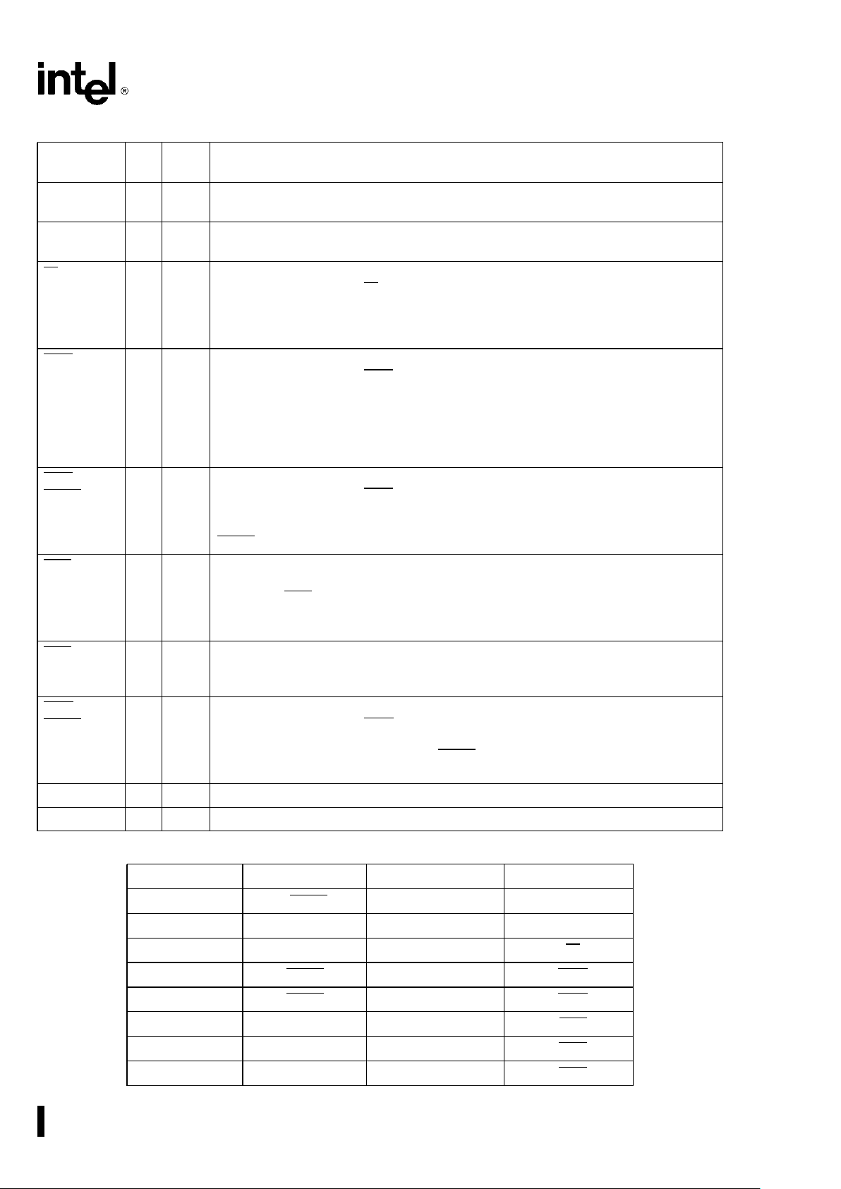
Table 1. Multifunction Pins
Pin
Ý
I/O Timing Modem
8 *OUT2 X2 Ð
9Ð*CLK/X1 Ð
10 Ð SCLK *RI
11 OUT0 TA *DSR
12 OUT1 ICLK *DCD
14 Ð Ð *CTS
15 Ð TB *DTR
16 Ð Ð *RTS
*Default
3
M82510
GENERAL DESCRIPTION
The M82510 can be functionally divided into seven
major blocks (See Fig 1): Bus Interface Unit, Timing
Unit, Modem Module, Tx FIFO, Rx FIFO, Tx Machine, and Rx Machine. Six of these blocks (all except Bus Interface Unit) can generate block interrupts. Three of these blocks can generate secondlevel interrupts which reflect errors/status within the
block (Receive Machine, Timing Unit, and the Modem Module).
The Bus interface unit allows the M82510 to interface with the rest of the system. It controls access to
device registers as well as generation of interrupts
to the external world. The FIFOs buffer the CPU
from the Serial Machines and reduce the interrupt
overhead normally required for serial operations.
The threshold (level of occupancy in the FIFO which
will generate an interrupt) is programmable for each
FIFO. The timing unit controls generation of the system clock through either its on-chip crystal oscillator,
or an externally generated clock. It also provides two
Baud Rate Generators/Timers with various options
and modes to support serial communication.
FUNCTIONAL DESCRIPTION
CPU Interface
The M82510 has a simple demultiplexed Bus Interface, which consists of a bidirectional three-state
eight-bit, data bus and a three-bit address bus. An
Interrupt pin along with the Read, Write and Chip
Select are the remaining signals used to interface
with the CPU. The three address lines along with the
Bank Pointer register are used to select the registers. The M82510 is designed to interface to all Intel
microprocessor and microcontroller families. Like
most other I/O based peripherals it is programmed
through its registers to support a variety of functions.
Its register set can be used in 8250A/16450 compatibility or High Performance modes. The 8250A/
16450 mode is the default wake-up mode in which
only the 8250A/16450 compatible registers are accessible. The remaining registers are default configured to support 8250A/16450 emulation.
Software Interface
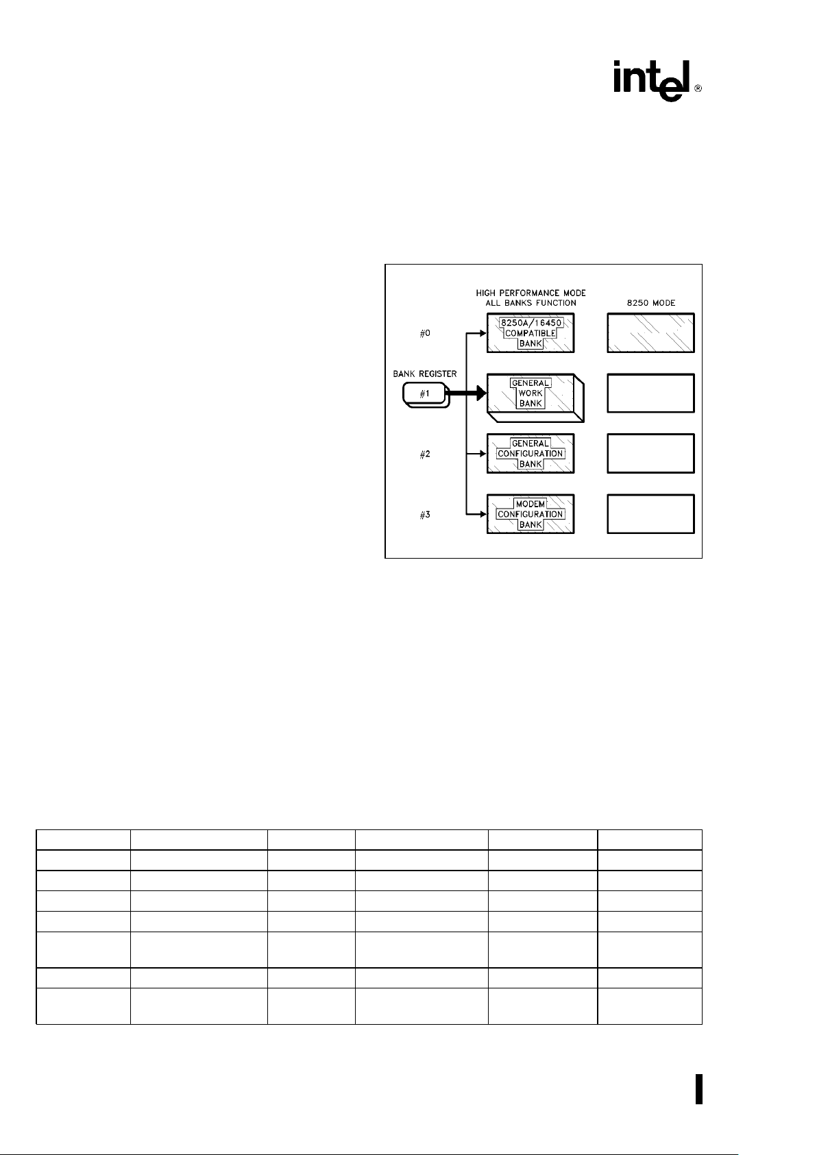
271072–3
Figure 3. M82510 Register Architecture
The M82510 is configured and controlled through its
35 registers which are divided into four banks. Only
one bank is accessible at any one time. The bank
switching is done by changing the contents of the
bank pointer (GIR/BANK – BANK0, BANK1). The
banks are logically grouped into 8250A/16450 compatible (0), General Work Bank (1), General Configuration (2), and Modem Configuration (3). The
8250A/16450 compatible bank (Bank 0) is the default bank upon power up.
The M82510 registers can be categorized under the
following:
Table 2. M82510 Register/Block Functions
Status Enable Configuration Command Data
FIFO FLR Ð FMD Ð Ð
MODEM MSR MIE PMD MCR Ð
RX RST, RXF RIE RMD RCM RXD, RXF
TX LSR LSR TMD TCM TXD, TXF
TIMER TMST TMIE CLCF, TMCR BBL, BBH
BACF, BBCF BAL, BAH
DEVICE GSR, GIR GER IMD ICM Ð
8250 LSR, MSR, GIR GER LCR, MCR MCR TXD, RXD
BAL, BAH
4

M82510
8250 Compatibility
Upon power up or reset, the M82510 comes up in the default wake up mode. The 8250A/16450 compatible
bank, bank zero, is the accessible bank and all the other registers are configured via their default values to
support this mode.
Table 3. 8250A/16450 Compatible Registers
M82510 Registers
8250A Registers
(Bank 0)
Address Read Write Read Write
00 (DLABe0) RxD TxD RBR THR
01 (DLABe0) GER GER IER IER
00 (DLABe1) BAL BAL DLL DLL
01 (DLABe1) BAH BAH DLM DLM
02 GIR/BANK BANK IIR Ð
03 LCR LCR LCR LCR
04 MCR MCR MCR MCR
05 LSR LSR LSR LSR
06 MSR MSR MSR MSR
07 ACR0 ACR0 SCR SCR
Table 4. Default Wake-Up Mode
RxD Ð ACR1 00H RxF Ð
TxD Ð RIE 1EH TxF Ð
BAL 02H RMD 00H TMST 30H
BAH 00H CLCF 00H TMCR Ð
GER 00H BACF 04H FLR 00H
GIR/BANK 01H BBCF 84H RCM Ð
LCR 00H PMD FCH TCM Ð
MCR 00H MIE 0FH GSR 12H
LSR 60H TMIE 00H ICM Ð
MSR 00H BBL 05H FMD 00H
ACR0 00H BBH 00H TMD 00H
RST 00H IMD 0CH
5
M82510
271072–4
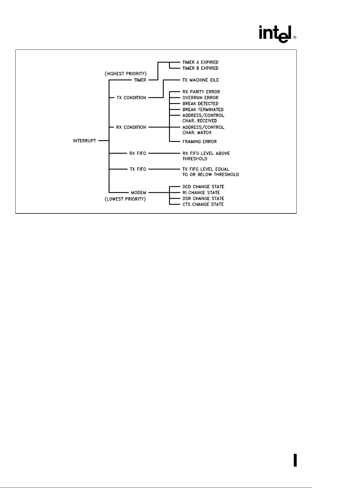
Figure 4. Interrupt Structure
Interrupts
There are two levels of interrupt/status reporting
within the M82510. The first level is the block level
interrupts such as RX FIFO, Tx FIFO, Rx Machine,
Tx Machine, Timing unit, and Modem Module. The
status of these blocks is reported in the General
Status and General Interrupt Registers. The second
level is the various sources within each block; only
three of the blocks generate second level interrupts
(Rx Machine, Timing Unit, and Modem Module). Interrupt requests are maskable at both the block level
and at the individual source level within the module.
If more than one unmasked block requests interrupt
service an on-chip interrupt controller will resolve
contention on a priority basis (each block has a fixed
priority). An interrupt request from a particular block
is activated if one of the unmasked status bits within
the status register for the block is set. A CPU service
operation, e.g., reading the appropriate status register, will reset the status bits.
ACKNOWLEDGE MODES
The interrupt logic will assert the INT pin when an
interrupt is coded into the General Interrupt register.
The INT pin is forced low upon acknowledgment.
The M82510 has two modes of interrupt acknowledgment:
1. Manual Acknowledge
The CPU must issue an explicit Interrupt Acknowledge command via the Interrupt Acknowledge bit of
the Internal Command register. As a result the INT
pin is forced low for two clocks and then updated.
2. Automatic Acknowledge
As opposed to the Manual Acknowledge mode,
when the CPU must issue an explicit interrupt acknowledge command, an interrupt service operation
is considered as an automatic acknowledgment.
This forces the INT pin low for two clock cycles.
After two cycles the INT pin is updated, i.e., if there
is still an active non-masked interrupt request the
INT pin is set HIGH.
INTERRUPT SERVICE
A service operation is an operation performed by the
CPU, which causes the source of the M82510 interrupt to be reset (it will reset the particular status bit
causing the interrupt). An interrupt request within the
M82510 will not reset until the interrupt source has
been serviced. Each source can be serviced in two
or three different ways; one general way is to disable
the particular status bit causing the interrupt, via the
corresponding block enable register. Setting the appropriate bit of the enable register to zero will mask
off the corresponding bit in the status register, thus
causing an edge on the input line to the interrupt
logic. The same effect can be achieved by masking
6
M82510
off the particular block interrupt request in GSR via
the
General Enable Register.
Another method,
which is applicable to all sources, is to issue the
Status Clear command from the
Internal Command
Register.
The detailed service requirements for each
source are given below:
Table 5. Service Procedures
Interrupt Status Bits Interrupt Specific
Source & Registers Masking Service
Timers TMST (1 – 0) TMIE (1 – 0) Read TMST
GSR (5) GER (5)
Tx GSR (4) GER (4) Write Character
Machine LSR (6) to tX FIFO
Rx LSR (4 – 1) RIE (7– 1) Read RST or
Machine RST (7 –1) GER (2) LSR Write 0
GSR (2) to bit in
RST/LSR
Rx FIFO RST/LSR (0) GER (0) Write 0 to
GSR (0) LSR/RST
Bit zero.
Read Character
Tx FIFO LSR (5) GER (1) Write to FIFO
GSR (1) Read GIR
(1)
Modem MSR (3-0) MIE (3-0) Read MSR
GSR (3) GER (3) write 0 into the
appropriate bits
of MSR (3 –0).
NOTE:
1. Only if pending interrupt is Tx FIFO.
System Clock Generation
The M82510 has two modes of System Clock Operation. It can accept an externally generated clock, or
it can use a crystal to internally generate its system
clock.
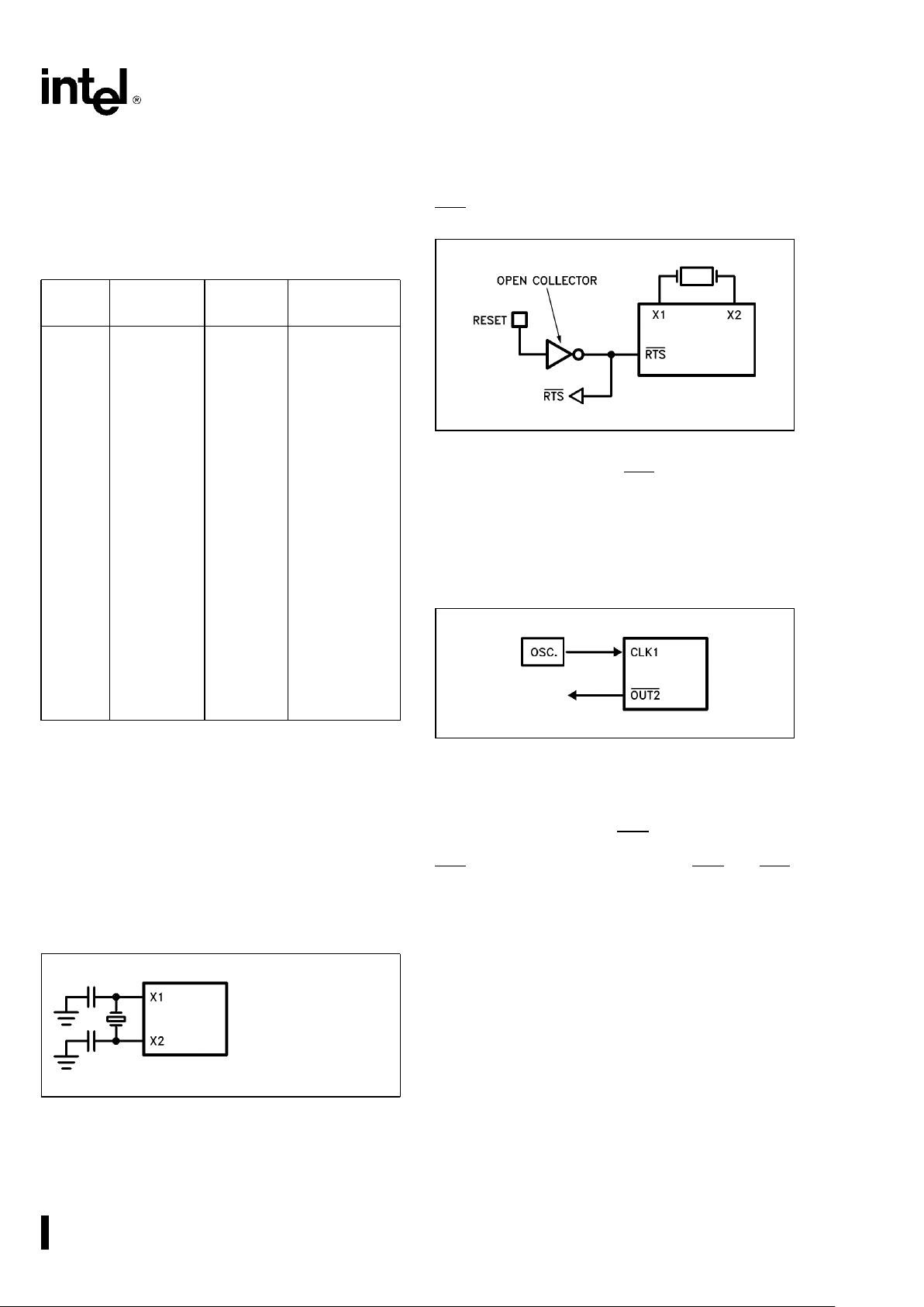
CRYSTAL OSCILLATOR
Parallel Resonant Crystal
271072–5
Figure 5. Crystal Oscillator
The M82510 has an on-chip oscillator to generate its
system clock. The oscillator will take the inputs from
a crystal attached to the X1 and X2 pins. This mode
is configured via a hardware strapping option on
RTS
.
271072–6
Figure 6. Strapping Option
During hardware reset the RTS
pin is an input; it is
weakly pulled high from within and then checked. If it
is driven low externally then the M82510 is configured for the Crystal Oscillator; otherwise an external
clock is expected.
EXTERNALLY GENERATED SYSTEM CLOCK
271072–7
Figure 7. External Clock
This is the default configuration. Under normal conditions the system clock is divided by two; however,
the user may disable divide by two via a hardware
strapping option on the DTR
pin. The Hardware
strapping option is similar to the one used on the
RTS
pin. It is forbidden to strap both DTR and RTS.
Transmit
The two major blocks involved in transmission are
the Transmit FIFO and the Transmit Machine. The
Tx FIFO acts as a buffer between the CPU and the
Tx Machine. Whenever a data character is written to
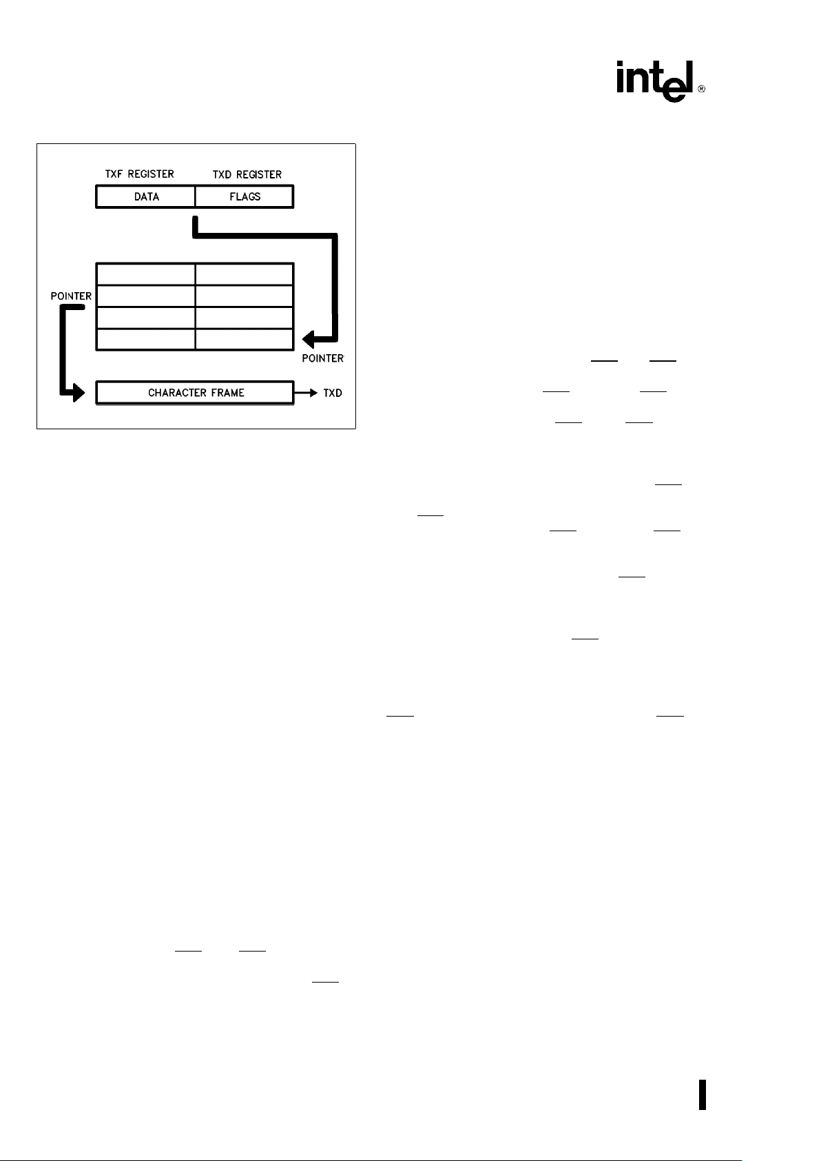
the Transmit Data register, it, along with the Transmit Flags (if applicable), is loaded into the Tx FIFO.
7
M82510
TX FIFO
271072–8
Figure 8. Tx FIFO
The Tx FIFO can hold up to four, eleven-bit characters (nine-bits data, parity, and address flag). It has
separate read and write mechanisms. The read and
write pointers are incremented after every operation
to allow data transfer to occur in a First In First Out
fashion. The Tx FIFO will generate a maskable interrupt when the level in the FIFO is below, or equal to,
the Threshold. The threshold is user programmable.
For example, if the threshold equals two, and the
number of characters in the Tx FIFO decreases from
three to two, the FIFO will generate an interrupt. The
threshold should be selected with regard to the system’s interrupt service latency.
NOTE:
There is a one character transmission delay between FIFO empty and Transmitter Idle, so a
threshold of zero may be selected without getting
an underrun condition. Also if more than four characters are written to the FIFO an overrun will occur
and the extra character will not be written to the Tx
FIFO. This error will not be reported to the CPU.
TX MACHINE
The Tx Machine reads characters from the Tx FIFO,
serializes the bits, and transmits them over the TXD
pin according to the timing signals provided for
transmission. It will also generate parity, transmit
break (upon CPU request), and manage the modem
handshaking signals (CTS
and RTS) if configured
so. The Tx machine can be enabled or disabled
through the Transmit Command register or CTS
.If
the transmitter is disabled in the middle of a character transmission the transmission will continue until
the end of the character; only then will it enter the
disable state.
TRANSMIT CLOCKS
There are two modes of transmission clocking, 1X
and 16X. In the 1X mode the transmitted data is
synchronous to the transmit clock as supplied by the
SCLK pin. In this mode stop-bit length is restricted to
one or two bits only. In the 16X mode the data is not
required to be synchronous to the clock. (Note: The
Tx clock can be generated by the BRGs or from the
SCLK pin.)
MODEM HANDSHAKING
The transmitter has three modes of handshaking.
Manual ModeÐIn this mode the CTS
and RTS pins
are not used by the Tx Machine (transmission is
started regardless of the CTS
state, and RTS is not
forced low). The CPU may manage the handshake
itself, by accessing the CTS
and RTS signals
through the MODEM CONTROL and MODEM
STATUS registers.
Semi-Automatic ModeÐIn this mode the RTS
pin
is activated whenever the transmitter is enabled.
The CTS
pin’s state controls transmission. Trans-
mission is enabled only if CTS
is active. If CTS becomes inactive during transmission, the Tx Machine
will complete transmission of the current character
and then go to the inactive state until CTS
becomes
active again.
Automatic ModeÐThis mode is similar to the semiautomatic mode, except that RTS
will be activated
as long as the transmitter is enabled and there are
more characters to transmit. The CPU need only fill
the FIFO, the handshake is done by the Tx Machine.
When both the shift register and the FIFO are empty
RTS
automatically goes inactive. (Note: The RTS pin
can be forced to the active state by the CPU, regardless of the handshaking mode, via the MODEM
CONTROL register.)
Receive
The M82510 reception mechanism involves two major blocks; the Rx Machine and the Rx FIFO. The Rx
Machine will assemble the incoming character and
its associated flags and then LOAD them on to the
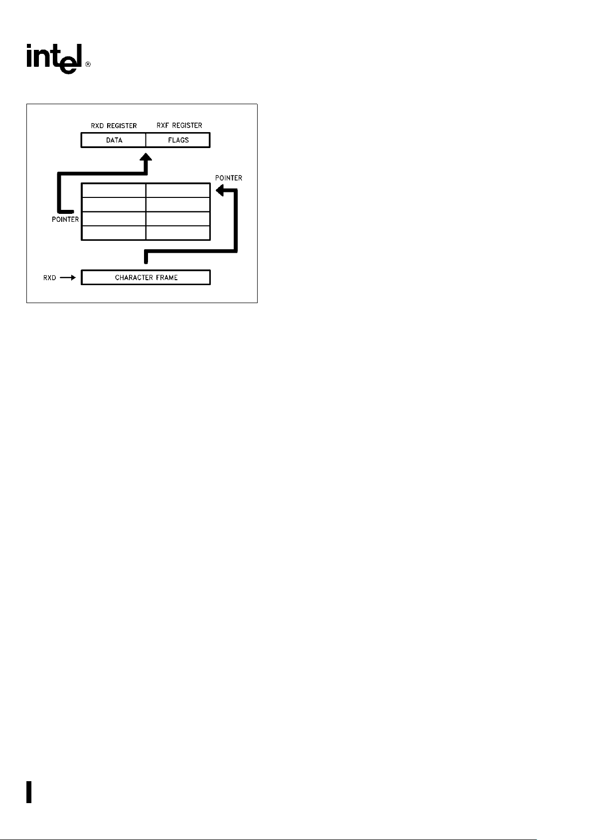
Rx FIFO. The top of the FIFO may be read by reading the Receive Data register and the Receive Flags
Register. The receive operation can be done in two
modes. In the
normal
mode the characters are received in the standard Asynchronous format and
only control characters are recognized. In the
ulan
mode, the nine bit protocol of the MCS-51 family is
supported and the ulan Address characters, rather
than Control Characters are recognized.
8
M82510
RX FIFO
271072–9
Figure 9. Rx FIFO
The Rx FIFO is very similar in structure and basic
operation to the Tx FIFO. It will generate a maskable
interrupt when the FIFO level is above, the threshold. The Rx FIFO can also be configured to operate
as a one-byte buffer. This mode is used for 8250
compatible software drivers. An overrun will occur
when the FIFO is full and the Rx Machine has a new
character for the FIFO. In this situation the oldest
character is discarded and the new character is
loaded from the Rx Machine. An Overrun error bit
will also be set in the RECEIVE STATUS and LINE
STATUS registers.
The user has the option to disable the loading of
incoming characters on to the Rx FIFO by using the
UNLOCK/LOCK FIFO commands. (See RECEIVE
COMMAND register.) When the Rx FIFO is locked, it
will ignore load requests from the Rx Machine, and
thus the received characters will not be loaded into
the FIFO and may be lost (if another character is
received). These two commands are useful when
the CPU is not willing to receive characters, or is
waiting for specific Control/Address characters. In
uLAN mode there are three options of address recognition, each of these options varies in the amount
of CPU offload, and degree of FIFO control through
OPEN/LOCK FIFO commands.
Automatic ModeÐIn this mode the Rx Machine will
open the FIFO whenever an Address Match occurs;
it will LOCK the FIFO if an address mismatch occurs.
Semi-Automatic ModeÐIn this mode the Rx Machine will open the FIFO whenever an address character is received. It will not lock the FIFO if the Address does not match. The user is responsible for
locking the Rx FIFO.
Manual ModeÐIn this mode the Rx Machine does
not control the FIFO automatically; however, the
user may UNLOCK/LOCK the FIFO by using the
RECEIVE COMMAND register.
RX MACHINE
The RX Machine has two modes of clocking the incoming dataÐ16X or 1X. In 16X synchronization is
done internally; in the 1X mode the data must be
synchronous to the SCLK pin input. The Rx Machine
synchronizes the data, passes it through a digital filter to filter out the spikes, and then uses the voting
counter to generate the data bit (multiple sampling
of input RXD). Bit polarity decisions are made on the
basis of majority voting; i.e., if the majority of the
samples are ‘‘1’’ the result is a ‘‘1’’ bit. If all samples
are not in agreement then the bit is also reported as
a noisy bit in the RECEIVE FLAGS register. The
sampling window is programmable for either 3/16 or
7/16 samples. The 3/16 mode is useful for high frequency transmissions, or when serious RC delays
are expected on the channel. The 7/16 is best suited for noisy media. The Rx machine also has a
DPLL to overcome frequency shift problems; however, using it in a very noisy environment may increase
the error, so the user can disable the DPLL via the
Receive Mode register. The Rx Machine will generate the parity and the address marker as well as any
framing error indications.
Start Bit DetectionÐThe falling edge of the Start
bit resets the DPLL counter and the Rx Machine
starts sampling the input line (the number of samples is determined by the configuration of the sampling window mode). The Start bit verification can be
done through either a majority voting system or an
absolute voting system. The absolute voting requires
that all the samples be in agreement. If one of the
samples does not agree then a false Start bit is determined and the Rx Machine returns to the Start Bit
search Mode. Once a Start bit is detected the Rx
Machine will use the majority voting sampling window to receive the data bits.
Break DetectionÐIf the input is low for the entire
character frame including the stop Bit, then the Rx
Machine will set Break Detected as well as Framing
Error in the RECEIVE STATUS and LINE STATUS
registers. It will push a NULL character onto the Rx
FIFO with a framing-error and Break flag (As part of
the Receive Flags). The Rx Machine then enters the
Idle state. When it sees a mark it will set Break Terminated in RECEIVE STATUS and LINE STATUS
registers and resume normal operation.
9

M82510
271072–10
Figure 10. Sampling Windows
Control CharactersÐThe Rx machine can gener-
ate a maskable interrupt upon reception of standard
ASCII or EBCDIC control characters, or an Address
marker is received in the uLAN mode. The Rx machine can also generate a maskable interrupt upon a
match with programmed characters in the Address/
Control Character 0 or Address/Control Character 1
registers.
Table 6. Control Character Recognition
CONTROL CHARACTER RECOGNITION
A
Ó
STANDARD SET
X
ASCII: 000X XXXXa0111 1111
(ASCII DEL)
(00 - 1FH
a
7 FH)
OR
X
EBCDIC: 00XX XXXX
(00 - 3FH)
B
Ó
User Programmed
X
ACR0, ACR1 XXXX XXXX
REGISTERS
Baud-Rate Generators/Timers
The M82510 has two-on-chip, 16-bit baud-rate generators. Each BRG can also be configured as a Timer, and is completely independent of the other. This
can be used when the Transmit and Receive baud
rates are different. The mode, the output, and the
source of each BRG is configurable, and can also be
optionally output to external devices via the TA, TB
pins (see Figure 11. BRG Sources and Outputs).
SOFTWARE
CONTROLLED
GATE
Rx CLK
SYS CLK
Tx CLK
SOURCE OUT
XTAL CLK
BRGB
SCLK
SOURCE
-A-
SOFTWARE
CONTROLLED
SCLK
GATE
SYS CLK
Rx CLK
XTAL CLK SOURCE OUT
Tx CLK
BRGA
-B-
OUTPUT
Figure 11. BRG Sources and Outputs
BAUD RATE GENERATION
The Baud Rate is generated by dividing the source
clock with the divisor count (from the Divisor count
registers). The count is loaded from the divisor count
registers into a count down register. A 50% duty cycle is generated by counting down in steps of two.
When the count is down to 2 the entire count is reloaded and the output clock is toggled. Optionally
the two BRGs may be cascaded to provide a larger
divisor.
f
0
e
f
in
./Divisor
wherefin is the input clock frequency and Divisor is
the count loaded into the appropriate count registers.
10
M82510
Table 7. Standard Baud Rates
Bit Rate 16x Divisor
%
Error
110 5236 (1474h) .007%
300 1,920 (780h) Ð
1200 480 (1E0h) Ð
2400 240 (F0h) Ð
9600 60 (3Ch) Ð
19,200 30 (1Eh) Ð
38,400 15 (0Fh) Ð
56,000 10 (0Ah) 2.8%
288,000 2 (02h) Ð
Source CLKeInternal Sys. Clk
e
18.432 MHz/2
e
9.216 MHz
The BRG counts down in increments of two and
then is divided by two to generate a 50% duty cycle;
however, for odd divisors it will count down the first
time by one. All subsequent countdowns will then
continue in steps of two. In those cases the duty
cycle is no longer exactly 50%. The deviation is given by the following equation:
deviatione1/(2Xdivisor)
The BRG can operate with any divisor between 1
and 65,535; however, for divisors between 1 and 3
the duty cycle is as follows:
Table 8. Duty Cycles
Divisor Duty Cycle
3 33%
2 50%
1 Same as Source
0 FORBIDDEN
Timer Mode
Each of the M82510 BRGs can be used as Timers.
The Timer is used to generate time delays by counting the internal system clock. When enabled the
Timer uses the count from the Divisor/Count registers to count down to 1. Upon terminal count a
maskable Timer Expired interrupt is generated. The
delay between the trigger and the terminal count is
given by the following equation:
DelayeCountX(System Clock Period)
To start counting, the Timer has to be triggered via
the Start Timer Command. To restart the Timer after
terminal count or while counting, the software has to
issue the trigger command again. While counting the
Timer can be enabled or disabled by using a software controlled Gate. It is also possible to output a
pulse generated upon terminal count through the TA
or TB pins.
In 1X clock mode the only clock source available is
the SCLK pin. The serial machines (both Tx Machine
and Rx Machine) can independently use one of two
clock modes, either 1X or 16X. Also no configuration
changes are allowed during operation as each write
in the BRG configuration registers causes a reset
signal to be sent to the BRG logic. The mode or
source clocks may be changed only after a Hardware or Software reset. The Divisor (or count, depending upon the mode) may be updated during operation unless the particular BRG machine is being
used as a clock source for one of the serial machines, and the particular serial machine is in operation at the time. Loading the count registers with ‘‘0’’
is forbidden in all cases, and loading it with a ‘‘1’’ is
forbidden in the Timer Mode only.
SERIAL DIAGNOSTICS
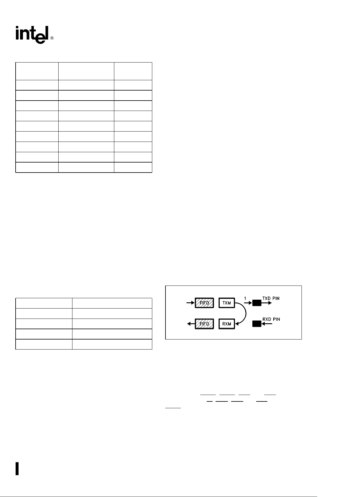
The M82510 supports two modes of Loopback operation, Local Loopback and Remote Loopback as
well as an Echo mode for diagnostics and improved
throughput.
LOCAL LOOPBACK
271072–11
Figure 12. Local Loopback
The Tx Machine output and Rx Machine input are
shorted internally, TXD pin output is held at Mark.
This feature allows simulation of Transmission/Reception of characters and checks the Tx FIFO, Tx
Machine, Rx Machine, and Rx FIFO along with the
software without any external side effects. The modem outputs OUT1
, OUT2, DTR and RTS are inter-
nally shorted to RI
, DCD, DSR and CTS respectively.
OUT0
is held at a mark state.
11
M82510
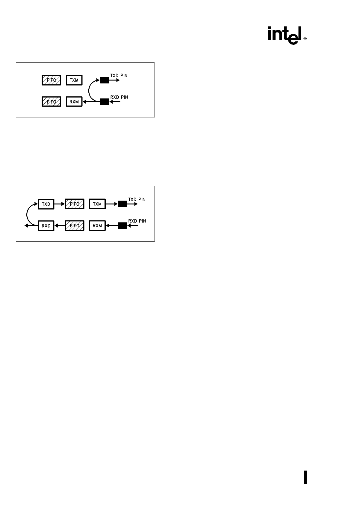
REMOTE LOOPBACK
271072–12
Figure 13. Remote Loopback
The TXD pin and RXD pin are shorted internally (the
data is not sent on to the RX Machine). This feature
allows the user to check the communications channel as well as the Tx and Rx pin circuits not checked
in the Local Loopback mode.
AUTO ECHO
271072–13
Figure 14. Auto Echo
In Echo Mode the received characters are automatically transmitted back. When the characters are
read from the Rx FIFO they are automatically
pushed back onto the Tx FIFO (the flags are also
included). The Rx Machine baud rate must be equal
to, or less than, the Tx Machine baud rate or some
of the characters may be lost. The user has an option of preventing echo of special characters; Control Characters and characters with Errors.
Power Down Mode
The M82510 has a ‘‘power down’’ mode to reduce
power consumption when the device is not in use.
The M82510 powers down when the power down
command is issued via the Internal Command Register (ICM). There are two modes of power down,
Sleep and Idle.
In Sleep mode, even the system clock of the
M82510 is shut down. The system clock source of
the M82510 can either be the Crystal Oscillator or
an external clock source. If the Crystal Oscillator is
being used and the power down command is issued,
then the M82510 will automatically enter the Sleep
mode. If an external clock is being used, then the
user must disable the external clock in addition to
issuing the Power Down command, to enter the
Sleep mode. The benefit of this mode is the increased savings in power consumption (typical power consumption in the Sleep mode is in the ranges of
100s of microAmps). However, upon wake up, the
user must reprogram the device. To exit this mode
the user can either issue a Hardware reset, or read
the FIFO Level Register (FLR) and then issue a software reset. In either case the contents of the
M82510 registers are not preserved and the device
must be reprogrammed prior to operation. If the
Crystal Oscillator is being used then the user must
allow enough time for the oscillator to wake up before issuing the software reset.
The M82510 is in the idle mode when the Power
Down command is issued and the system clock is
still running (i. e. the system clock is generated externally and not disabled by the user). In this mode
the contents of all registers and memory cells are
preserved, however, the power consumption in this
mode is greater than in the Sleep mode. Reading
FLR will take the M82510 out of this mode.
NOTE:
The data read from FLR when exiting Power Down
is invalid and should be ignored.
12
 Loading...