

Page 1
October 1993 Order Number: 271089-006
M80C196KB
16-BIT HIGH PERFORMANCE CHMOS
MICROCONTROLLER
Military
Y
232 Byte Register File
Y
Register-to-Register Architecture
Y
28 Interrupt Sources/16 Vectors
Y
2.3 ms 16 x 16 Multiply (12 MHz)
Y
4.0 ms 32/16 Divide (12 MHz)
Y
Powerdown and Idle Modes
Y
Five 8-Bit I/O Ports
Y
16-Bit Watchdog Timer
Y
Dynamically Configurable 8-Bit or
16-Bit Buswidth
Y
Available in 68-Lead PGA and 68-Lead
Ceramic Quad Flat Pack
Y
Full Duplex Serial Port
Y
High Speed I/O Subsystem
Y
16-Bit Timer
Y
16-Bit Up/Down Counter with Capture
Y
Pulse-Width-Modulated Output
Y
Four 16-Bit Software Timers
Y
10-Bit A/D Converter with S/H
Y
12 MHz Version Ð M80C196KB
Y
Available in Two Product Grades:
Ð MIL-STD-883,b55§Ctoa125§C(TC)
Ð Military Temperature Only (MTO),
b
55§Ctoa125§C(TC)
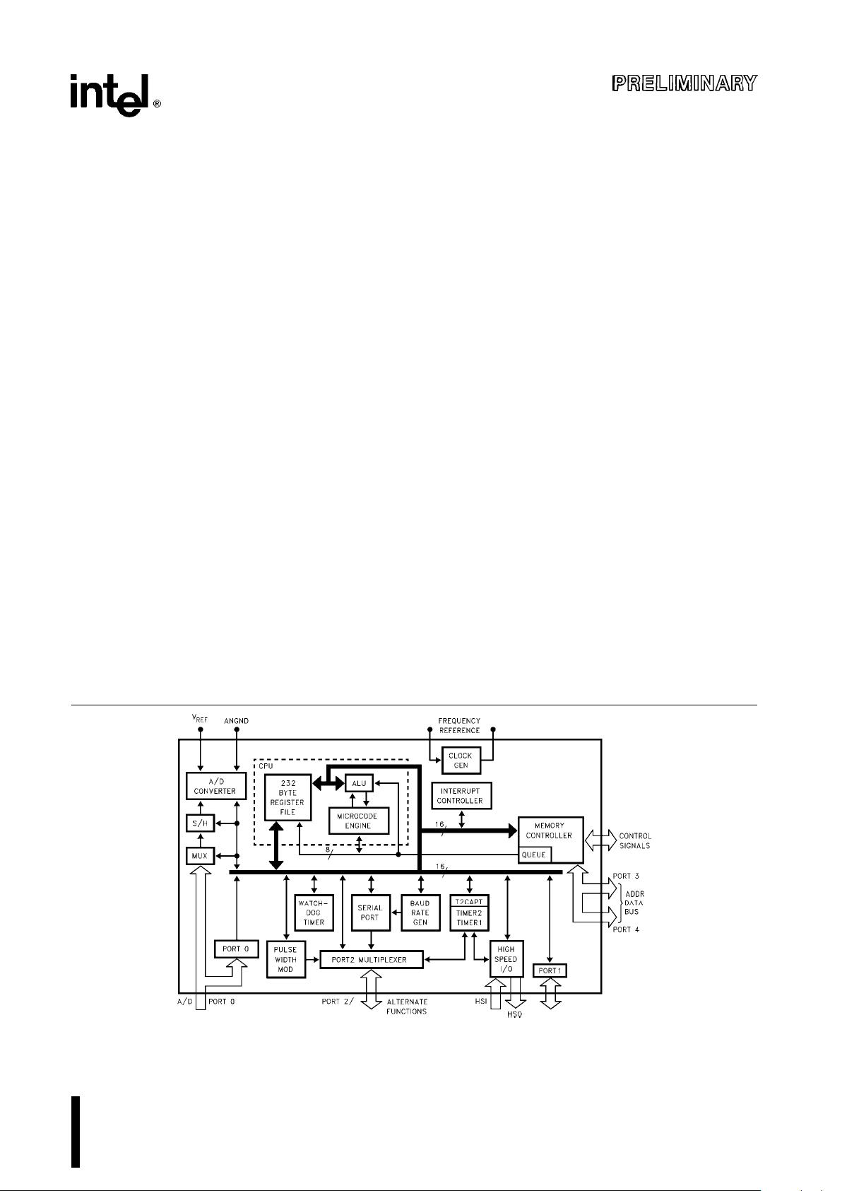
The M80C196KB 16-bit microcontroller is a high performance member of the MCSÉ-96 microcontroller family.
The M80C196KB is pin-for-pin compatible and uses a true superset of the M8096 instructions. Intel’s CHMOS
process provides a high performance processor along with low power consumption. To further reduce power
requirements, the processor can be placed into Idle or Powerdown Mode.
Bit, byte, word and some 32-bit operations are available on the M80C196KB. With a 12 MHz oscillator a 16-bit
addition takes 0.66 ms, and the instruction times average 0.5 ms to 1.5 ms in typical applications.
Four high-speed capture inputs are provided to record times when events occur. Six high-speed outputs are
available for pulse or waveform generation. The high-speed output can also generate four software timers or
start an A/D conversion. Events can be based on the timer or up/down counter.
Also provided on-chip are an A/D converter with Sample and Hold, serial port, watchdog timer, and a pulsewidth-modulated output signal.
271089–1
Figure 1. M80C196KB Block Diagram
Page 2

M80C196KB
ARCHITECTURE
The M80C196KB is a member of the MCSÉ-96 family, and as such has the same architecture and uses the
same instruction set as the M8096. Many new features have been added on the M80C196KB including:
CPU FEATURES
Divide by 2 instead of divide by 3 clock for 1.5X performance
Faster instructions, especially indexed/indirect data operations
2.33 ms16
c
16 multiply with 12 MHz clock (was 6.25 ms) on the 8096
Faster interrupt response (almost twice as fast as 8096)
Powerdown and Idle Modes
6 new instructions including Compare Long and Block Move
8 new interrupt vectors/6 new interrupt sources
PERIPHERAL FEATURES
SFR Window switching allows read-only registers to be written and vice-versa
Timer2 can count up or down by external selection
Timer2 has an independent capture register
HSO line events are stored in a register
HSO has CAM Lock and CAM Clear commands
New Baud Rate values are needed for serial port, higher speeds possible in all modes
Double buffered serial port transmit register
Serial Port Receive Overrun and Framing Error Detection
PWM has a Divide-by-2 Prescaler
2
Page 3

M80C196KB
NEW INSTRUCTIONS
PUSHA Ð PUSHes the PSW, IMASK, IMASK1, and WSR
(Used instead of PUSHF when new interrupts and registers are used.)
assembly language format: PUSHA
object code format:
k
11110100
l
bytes: 1
states: on-chip stack: 12
off-chip stack: 18
POPA Ð POPs the PSW, IMASK, IMASK1, and WSR
(Used instead of POPF when new interrupts and registers are used.)
assembly language format: POPA
object code format:
k
11110101
l
bytes: 1
states: on-chip stack: 12
off-chip stack:18
IDLPD Ð Sets the part into Idle or Powerdown Mode
assembly language format: IDLPD
Ý
key (keye1 for Idle, keye2 for Powerdown.)
object code format:k11110110lkkey
l
bytes: 2
states: legal key: 8
illegal key: 25
DJNZW Ð Decrement Jump Not Zero using a Word counter
assembly language format: DJNZW wreg, cadd
object code format:
k
11100001
lk
wreglkdisp
l
bytes: 3
states: jump not taken: 6
jump taken: 10
CMPL Ð Compare 2 long direct values
assembly language format: DST SRC
CMPL Lreg, Lreg
object code format:
k
11000101lksrc Lreglkdst Lreg
l
bytes: 3
states: 7
BMOV Ð Block move using 2 auto-incrementing pointers and a counter
assembly language format: PTRS CNTREG
BMOV Lreg, wreg
object code format:
k
11000001lkwreglkLreg
l
bytes: 3
states: internal/internal: 8 per transfera6
external/internal: 11 per transfer
a
6
external/external: 14 per transfer
a
6
3
Page 4

M80C196KB
SFR OPERATION
All of the registers that were present on the M8096 work the same way as they did, except that the baud rate
value is different. The new registers shown in the memory map control new functions. The most important new
register is the Window Select Register (WSR) which allows reading of the formerly write-only registers and
vice-versa. Using the WSR is described later in this data sheet.
4
Page 5
M80C196KB
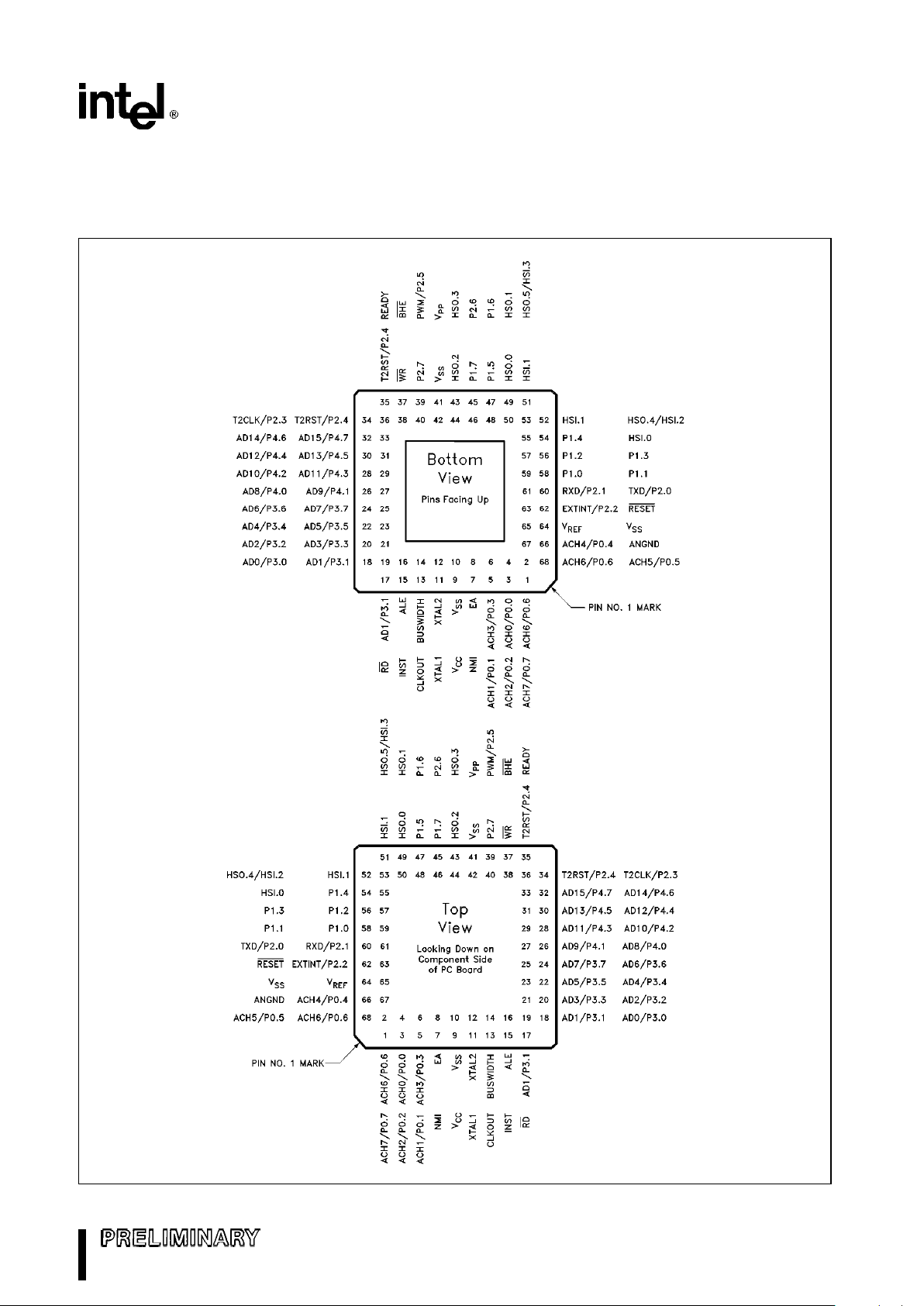
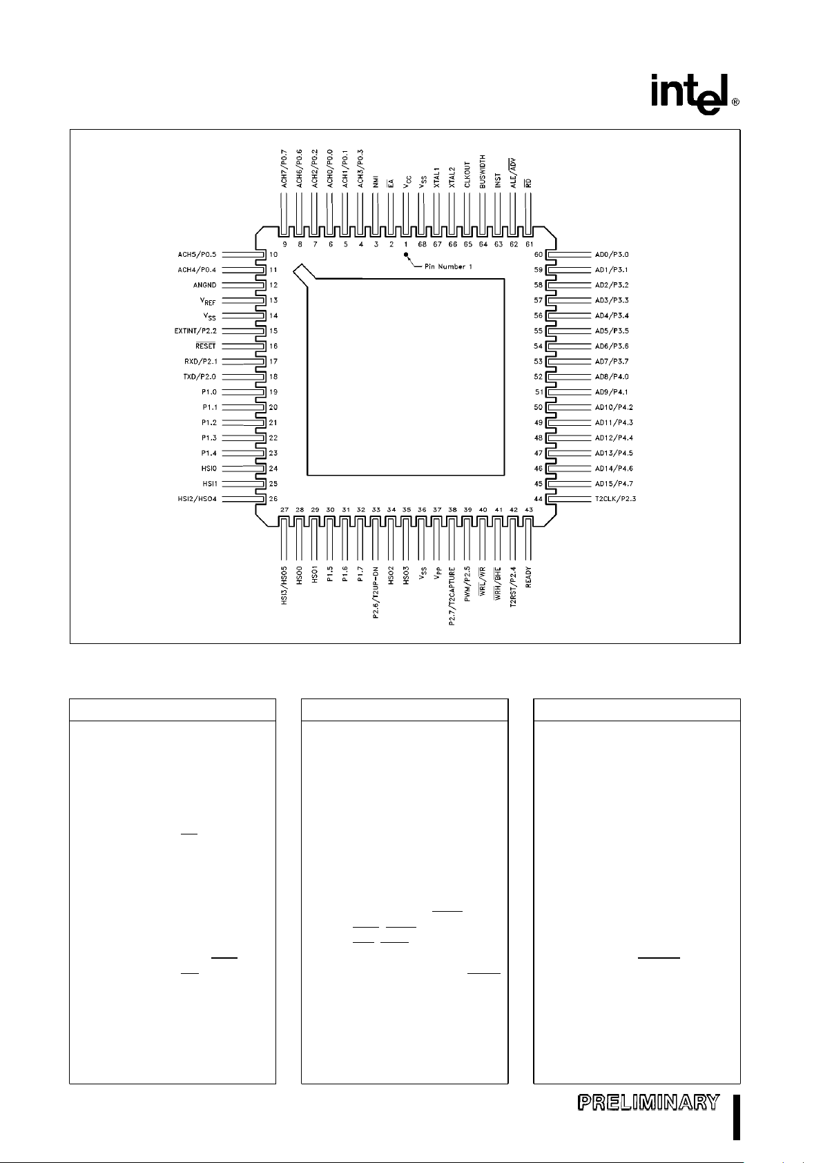
PACKAGING
The M80C196KB is available in a ceramic pin grid array, shown in Figure 2, and a leaded ceramic quad pack
shown in Figure 3. A comparison of the pinouts for both of these package types is shown in Tables 1a – 1c.
271089–2
Figure 2. Pin Grid Array Pinout
5
Page 6
M80C196KB
271089–3
Figure 3. 68-Lead Ceramic Quad Flat Pack Pinout
Table 1a. M80C196KB Pinout Ð in PGA Pin Order
PGA Signal
1 ACH7/P0.7
2 ACH6/P0.6
3 ACH2/P0.2
4 ACH0/P0.0
5 ACH1/P0.1
6 ACH3/P0.3
7 NMI
8EA
9V
CC
10 V
SS
11 XTAL1
12 XTAL2
13 CLKOUT
14 BUSWIDTH
15 INST
16 ALE/ADV
17 RD
18 AD0/P3.0
19 AD1/P3.1
20 AD2/P3.2
21 AD3/P3.3
22 AD4/P3.4
23 AD5/P3.5
PGA Signal
24 AD6/P3.6
25 AD7/P3.7
26 AD8/P4.0
27 AD9/P4.1
28 AD10/P4.2
29 AD11/P4.3
30 AD12/P4.4
31 AD13/P4.5
32 AD14/P4.6
33 AD15/P4.7
34 T2CLK/P2.3
35 READY
36 T2RST/P2.4/AINC
37 BHE/WRH
38 WR/WRL
39 PWM/P2.5
40 T2CAPTURE/P2.7/PACT
41 V
PP
42 V
SS
43 HS0.3
44 HS0.2
45 T2UP-DN/P2.6
46 P1.7
PGA Signal
47 P1.6
48 P1.5
49 HSO.1
50 HSO.0
51 HSO.5/HSI.3
52 HSO.4/HSI.2
53 HSI.1
54 HSI.0
55 P1.4
56 P1.3
57 P1.2
58 P1.1
59 P1.0
60 TXD/P2.0
61 RXD/P2.1
62 RESET
63 EXTINT/P2.2
64 V
SS
65 V
REF
66 ANGND
67 ACH4/P0.4
68 ACH5/P0.5
6
Page 7
M80C196KB
Table 1b. M80C196KB Pinout Ð in CQFP Pin Order
CQFP Signal
1V
CC
2EA
3 NMI
4 ACH3/P0.3
5 ACH1/P0.1
6 ACH0/P0.0
7 ACH2/P0.2
8 ACH6/P0.6
9 ACH7/P0.7
10 ACH5/P0.5
11 ACH4/P0.4
12 ANGND
13 V
REF
14 V
SS
15 EXTINT/P2.2
16 RESET
17 RXD/P2.1
18 TXD/P2.0
19 P1.0
20 P1.1
21 P1.2
22 P1.3
23 P1.4
CQFP Signal
24 HSI.0
25 HSI.1
26 HSO.4/HSI.2
27 HSO.5/HSI.3
28 HSO.0
29 HSO.1
30 P1.5
31 P1.6
32 P1.7
33 T2UP-DN/P2.6
34 HSO.2
35 HSO.3
36 V
SS
37 V
PP
38 T2CAPTURE/P2.7/PACT
39 PWM/P2.5
40 WR
/WRL
41 BHE/WRH
42 T2RST/P2.4/AINC
43 READY
44 T2CLK/P2.3
45 AD15/P4.7
46 AD14/P4.6
CQFP Signal
47 AD13/P4.5
48 AD12/P4.4
49 AD11/P4.3
50 AD10/P4.2
51 AD9/P4.1
52 AD8/P4.0
53 AD7/P3.7
54 AD6/P3.6
55 AD5/P3.5
56 AD4/P3.4
57 AD3/P3.3
58 AD2/P3.2
59 AD1/P3.1
60 AD0/P3.0
61 RD
62 ALE/ADV
63 INST
64 BUSWIDTH
65 CLKOUT
66 XTAL2
67 XTAL1
68 V
SS
Table 1c. M80C196KB Pinout Ð in Signal Order
Signal PGA CQFP
ACH0/P0.0 4 6
ACH1/P0.1 5 5
ACH2/P0.2 3 7
ACH3/P0.3 6 4
ACH4/P0.4 67 11
ACH5/P0.5 68 10
ACH6/P0.6 2 8
ACH7/P0.7 1 9
P1.0 59 19
P1.1 58 20
P1.2 57 21
P1.3 56 22
P1.4 55 23
P1.5 48 30
P1.6 47 31
P1.7 46 32
TXD/P2.0 60 18
RXD/P2.1 61 17
EXTINT/P2.2 63 15
T2CLK/P2.3 34 44
T2RST/P2.4/AINC 36 42
PWM/P2.5 39 39
T2UP-DN/P2.6 45 33
Signal PGA CQFP
T2CAPTURE/P2.7/PACT
40 38
AD0/P3.0 18 60
AD1/P3.1 19 59
AD2/P3.2 20 58
AD3/P3.3 21 57
AD4/P3.4 22 56
AD5/P3.5 23 55
AD6/P3.6 24 54
AD7/P3.7 25 53
AD8/P4.0 26 52
AD9/P4.1 27 51
AD10/P4.2 28 50
AD11/P4.3 29 49
AD12/P4.4 30 48
AD13/P4.5 31 47
AD14/P4.6 32 46
AD15/P4.7 33 45
HSO.0 50 28
HSO.1 49 29
HSO.2 44 34
HSO.3 43 35
HSO.4/HSI.2 52 26
HSO.5/HSI.3 51 27
Signal PGA CQFP
HSI.0 54 24
HSI.1 53 25
RD
17 61
WR
/WRL 38 40
BHE
/WRH 37 41
BUSWIDTH 14 64
ALE/ADV
16 62
EA
82
INST 15 63
READY 35 43
NMI 7 3
RESET
62 16
XTAL1 11 67
XTAL2 12 66
CLKOUT 13 65
ANGND 66 12
V
REF
65 13
V
PP
41 37
V
CC
91
V
SS
10 68
V
SS
42 36
V
SS
64 14
7
Page 8
M80C196KB
PIN DESCRIPTIONS
Symbol Name and Function
V
CC
Main supply voltage (5V).
V
SS
Digital circuit ground (0V). There are three VSSpins, all of which must be connected.
V
REF
Reference voltage for the A/D converter (5V). V
REF
is also the supply voltage to the
analog portion of the A/D converter and the logic used to read Port 0. Must be connected
for A/D and Port 0 to function.
ANGND Reference ground for the A/D converter. Must be held at nominally the same potential as
V
SS
.
V
PP
Timing pin for the return from powerdown circuit. Connect this pin with a 1 mF capacitor to
V
SS
anda1MXresistor to VCC. If this function is not used VPPmay be tied to VCC. This
pin was V
BB
on the 8X9X-90 parts and is the programming voltage on EPROM part.
XTAL1 Input of the oscillator inverter and of the internal clock generator.
XTAL2 Output of the oscillator inverter.
CLKOUT Output of the internal clock generator. The frequency of CLKOUT is (/2 the oscillator
frequency. It has a 50% duty cycle.
RESET Reset input to the chip. Input low for at least 4 state times to reset the chip. The
subsequent low-to-high transition re- synchronizes CLKOUT and commences a 10-statetime sequence in which the PSW is cleared, a byte read from 2018H loads CCR, and a
jump to location 2080H is executed. Input high for normal operation. RESET has an
internal pullup.
BUSWIDTH Input for buswidth selection. If CCR bit 1 is a one, this pin selects the bus width for the bus
cycle in progress. If BUSWIDTH is a 1, a 16-bit bus cycle occurs. If BUSWIDTH isa0an
8-bit cycle occurs. If CCR bit 1 is a 0, the bus is always an 8-bit bus. This pin is the TEST
pin on 8X9X-90 parts. Systems with TEST tied to VCCdo not need to change.
8
Page 9
M80C196KB
PIN DESCRIPTIONS (Continued)
Symbol Name and Function
NMI A positive transition causes a vector through 203EH.
INST Output high during an external memory read indicates the read is an instruction fetch. INST
is valid throughout the bus cycle. INST is activated only during external memory accesses
and output low for a data fetch.
EA EA must be equal to a TTL-low to cause address locations 2000H through 3FFFH to be
directed to off-chip memory.
ALE/ADV Address Latch Enable or Address Valid output, as selected by CCR. Both pin options
provide a latch to demultiplex the address from the address/data bus. When the pin is
ADV
, it goes inactive high at the end of the bus cycle. ADV can be used as a chip select for
external memory. ALE/ADV
is activated only during external memory accesses.
RD Read signal output to external memory. RD is activated only during external memory
reads.
WR/WRL Write and Write Low output to external memory, as selected by the CCR. WR will go low
for every external write, while WRL
will go low only for external writes where an even byte
is being written. WR
/WRL is activated only during external memory writes.
BHE/WRH Bus High Enable or Write High output to external memory, as selected by the CCR. BHE
e
0 selects the bank of memory that is connected to the high byte of the data bus. A0e0
selects the bank of memory that is connected to the low byte of the data bus. Thus
accesses to a 16-bit wide memory can be to the low byte only (A0e0, BHEe1), to the
high byte only (A0
e
1, BHEe0), or both bytes (A0e0, BHEe0). If the WRH function
is selected, the pin will go low if the bus cycle is writing to an odd memory location. BHE
/
WRH
is valid only during 16-bit external memory write cycles.
READY Ready input to lengthen external memory cycles, for interfacing to slow or dynamic
memory, or for bus sharing. If the pin is high, CPU operation continues in a normal manner.
If the pin is low prior to the falling edge of CLKOUT, the memory controller goes into a wait
mode until the next positive transition in CLKOUT occurs with READY high. When the
external memory is not being used, READY has no effect. Internal control of the number of
wait states inserted into a bus cycle held not ready is available through configuration of
CCR.
HSI Inputs to High Speed Input Unit. Four HSI pins are available: HSI.0, HSI.1, HSI.2, and
HSI.3. Two of them (HSI.2 and HSI.3) are shared with the HSO Unit.
HSO Outputs from High Speed Output Unit. Six HSO pins are available: HSO.0, HSO.1, HSO.2,
HSO.3, HSO.4, and HSO.5. Two of them (HSO.4 and HSO.5) are shared with the HSI Unit.
Port 0 8-bit high impedance input-only port. Three pins can be used as digital inputs and/or as
analog inputs to the on-chip A/D converter.
Port 1 8-bit quasi-bidirectional I/O port.
Port 2 8-bit multi-functional port. All of its pins are shared with other functions in the M80C196KB.
Ports 3 and 4 8-bit bi-directional I/O ports with open drain outputs. These pins are shared with the
multiplexed address/data bus which has strong internal pullups.
9
Page 10

M80C196KB
Instruction Summary
Mnemonic Operands Operation (Note 1)
Flags
Notes
Z N C V VT ST
ADD/ADDB 2 D
w
DaA
&&&&
u
b
ADD/ADDB 3 D
w
BaA
&&&&
u
b
ADDC/ADDCB 2 D
w
DaAaC
v
&&&
u
b
SUB/SUBB 2 D
w
DbA
&&&&
u
b
SUB/SUBB 3 D
w
BbA
&&&&
u
b
SUBC/SUBCB 2 D
w
DbAaCb1
v
&&&
u
b
CMP/CMPB 2 DbA
&&&&
u
b
MUL/MULU 2 D,Da2
w
DcA
bbbbb b
2
MUL/MULU 3 D,Da2
w
BcA
bbbbb b
2
MULB/MULUB 2 D,Da1
w
DcA
bbbbb b
3
MULB/MULUB 3 D,Da1
w
BcA
bbbbb b
3
DIVU 2 D
w
(D,Da2) /A,Da2
w
remainder
bbb
&
u
b
2
DIVUB 2 D
w
(D,Da1) /A,Da1
w
remainder
bbb
&
u
b
3
DIV 2 D
w
(D,Da2) /A,Da2
w
remainder
bbb
&
u
b
DIVB 2 D
w
(D,Da1) /A,Da1
w
remainder
bbb
&
u
b
AND/ANDB 2 D
w
D AND A
&&
00
bb
AND/ANDB 3 D
w
B AND A
&&
00
bb
OR/ORB 2 D
w
DORA
&&
00
bb
XOR/XORB 2 D
w
D (ecxl. or) A
&&
00
bb
LD/LDB 2 D
w
A
bbbbb b
ST/STB 2 A
w
D
bbbbb b
LDBSE 2 D
w
A; Da1
w
SIGN(A)
bbbbb b
3,4
LDBZE 2 D
w
A; Da1
w
0
bbbbb b
3,4
PUSH 1 SP
w
SPb2; (SP)
w
A
bbbbb b
POP 1 A
w
(SP); SPa2
bbbbb b
PUSHF 0 SP
w
SPb2; (SP)
w
PSW; 0 0 0 0 0 0
PSW
w
0000H; I
w
0
POPF 0 PSW
w
(SP); SP
w
SPa2; I
w
& & &&& & &
SJMP 1 PC
w
PCa11-bit offset
bbbbb b
5
LJMP 1 PC
w
PCa16-bit offset
bbbbb b
5
BR[indirect
]
1PC
w
(A)
bbbbb b
SCALL 1 SP
w
SPb2;
bbbbb b
5
(SP)
w
PC; PC
w
PCa11-bit offset
LCALL 1 SP
w
SPb2; (SP)
w
PC;
bbbbb b
5
PC
w
PCa16-bit offset
10
Page 11

M80C196KB
Instruction Summary (Continued)
Mnemonic Operands Operation (Note 1)
Flags
Notes
Z N C V VT ST
RET 0 PC
w
(SP); SP
w
SPa2
bbbb b b
J (conditional) 1 PC
w
PCa8-bit offset (if taken)
bbbb b b
5
JC 1 Jump if Ce1
bbbb b b
5
JNC 1 jump if Ce0
bbbb b b
5
JE 1 jump if Ze1
bbbb b b
5
JNE 1 Jump if Ze0
bbbb b b
5
JGE 1 Jump if Ne0
bbbb b b
5
JLT 1 Jump if Ne1
bbbb b b
5
JGT 1 Jump if Ne0 and Ze0
bbbb b b
5
JLE 1 Jump if Ne1orZe1
bbbb b b
5
JH 1 Jump if Ce1 and Ze0
bbbb b b
5
JNH 1 Jump if Ce0orZe1
bbbb b b
5
JV 1 Jump if Ve0
bbbb b b
5
JNV 1 Jump if Ve1
bbbb b b
5
JVT 1 Jump if VTe1; Clear VT
bbbb
0
b
5
JNVT 1 Jump if VTe0; Clear VT
bbbb
0
b
5
JST 1 Jump if STe1
bbbb b b
5
JNST 1 Jump if STe0
bbbb b b
5
JBS 3 Jump if Specified Bite1
bbbb b b
5,6
JBC 3 Jump if Specified Bite0
bbbb b b
5,6
DJNZ/ 1 D
w
Db1;
bbbb b b
5
DJNZW If D
i
0 then PC
w
PCa8-bit offset
DEC/DECB 1 D
w
Db1
&&&&
u
b
NEG/NEGB 1 D
w
0bD
&&&&
u
b
INC/INCB 1 D
w
Da1
&&&&
u
b
EXT 1 D
w
D; Da2
w
Sign (D)
&&
00
bb
2
EXTB 1 D
w
D; Da1
w
Sign (D)
&&
00
bb
3
NOT/NOTB 1 D
w
Logical Not (D)
&&
00
bb
CLR/CLRB 1 D
w
0 1000
bb
SHL/SHLB/SHLL 2 C
w
msb-----lsb
w
0
&&&&
u
b
7
SHR/SHRB/SHRL 2 0
x
msb-----lsb
x
C
&&&
0
b
&
7
SHRA/SHRAB/SHRAL 2 msb
x
msb-----lsb
x
C
&&&
0
b
&
7
SETC 0 C
w
1
bb1bb b
CLRC 0 C
w
0
bb0bb b
11
Page 12

M80C196KB
Instruction Summary (Continued)
Mnemonic Operands Operation (Note 1)
Flags
Notes
Z N C V VT ST
CLRVT 0 VT
w
0
bbbb
0
b
RST 0 PC
w
2080H 0 0 0 0 0 0 8
DI 0 Disable All Interupts (I
w
0)
bbbb b b
EI 0 Enable All Interupts (I
w
1)
bbbb b b
NOP 0 PC
w
PCa1
bbbb b b
SKIP 0 PC
w
PCa2
bbbb b b
NORML 2 Left shift till msbe1; D
w
shift count
&&
0
bb b
7
TRAP 0 SP
w
SPb2;
bbbb b b
9
(SP)
w
PC; PC
w
(2010H)
PUSHA 1 SP
w
SP-2; (SP)
w
PSW; 0 0 0 0 0 0
PSW
w
0000H; SP
w
SP-2;
(SP)
w
IMASK1/WSR; IMASK1
w
00H
POPA 1 IMASK1/WSR
w
(SP); SP
w
SPa2
&&&& & &
PSW
w
(SP); SP
w
SPa2
IDLPD 1 IDLE MODE IF KEYe1;
bbbb b b
POWERDOWN MODE IF KEYe2;
CHIP RESET OTHERWISE
CMPL 2 D-A
&&&&
u
b
BMOV 2
[
PTRÐHI
]
a
w
[
PTRÐLOW
]
a
;
bbbb b b
UNTIL COUNTe0
NOTES:
1. If the mnemonic ends in ‘‘B’’ a byte operation is performed, otherwise a word operation is done. Operands D, B, and A
must conform to the alignment rules for the required operand type. D and B are locations in the Register File; A can be
located anywhere in memory.
2. D,D
a
2 are consecutive WORDS in memory; D is DOUBLE-WORD aligned.
3. D,D
a
1 are consecutive BYTES in memory; D is WORD aligned.
4. Changes a byte to word.
5. Offset is a 2’s complement number.
6. Specified bit is one of the 2048 bits in the register file.
7. The ‘‘L’’ (Long) suffix indicates double-word operation.
8. Initiates a Reset by pulling RESET
low. Software should re-initialize all the necessary registers with code starting at 2080H.
9. The assembler will not accept this mnemonic.
12
Page 13

M80C196KB
Instruction Execution State Times (Minimum)
(1)
MNEMONIC DIRECT IMMED
INDIRECT INDEXED
NORMAL* A-INC* SHORT* LONG*
ADD (3-op) 5 6 7/10 8/11 7/10 8/11
SUB (3-op) 5 6 7/10 8/11 7/10 8/11
ADD (2-op) 4 5 6/8 7/9 6/8 7/9
SUB (2-op) 4 5 6/8 7/9 6/8 7/9
ADDC 4 5 6/8 7/9 6/8 7/9
SUBC 4 5 6/8 7/9 6/8 7/9
CMP 4 5 6/8 7/9 6/8 7/9
ADDB (3-op) 5 5 7/10 8/11 7/10 8/11
SUBB (3-op) 5 5 7/10 8/11 7/10 8/11
ADDB (2-op) 4 4 6/8 7/9 6/8 7/9
SUBB (2-op) 4 4 6/8 7/9 6/8 7/9
ADDCB 4 4 6/8 7/9 6/8 7/9
SUBCB 4 4 6/8 7/9 6/8 7/9
CMPB 4 4 6/8 7/9 6/8 7/9
MUL (3-op) 16 17 18/21 19/22 19/22 20/23
MULU (3-op) 14 15 16/19 17/19 17/20 18/21
MUL (2-op) 16 17 18/21 19/22 19/22 20/23
MULU (2-op) 14 15 16/19 17/19 17/20 18/21
DIV 26 27 28/31 29/32 29/32 30/33
DIVU 24 25 26/29 27/30 27/30 28/31
MULB (3-op) 12 12 14/17 15/18 15/18 16/19
MULUB (3-op) 10 10 12/15 13/15 12/16 14/17
MULB (2-op) 12 12 14/17 15/18 15/18 16/19
MULUB (2-op) 10 10 12/15 13/15 12/16 14/17
DIVB 18 18 20/23 21/24 21/24 22/25
DIVUB 16 16 18/21 19/22 19/22 20/23
AND (3-op) 5 6 7/10 8/11 7/10 8/11
AND (2-op) 4 5 6/8 7/9 6/8 7/9
OR (2-op) 4 5 6/8 7/9 6/8 7/9
XOR 4 5 6/8 7/9 6/8 7/9
ANDB (3-op) 5 5 7/10 8/11 7/10 8/11
ANDB (2-op) 4 4 6/8 7/9 6/8 7/9
ORB (2-op) 4 4 6/8 7/9 6/8 7/9
XORB 4 4 6/8 7/9 6/8 7/9
LD/LDB 4 5 5/8 6/8 6/9 7/10
ST/STB 4 5 5/8 6/9 6/9 7/10
LDBSE 4 4 5/8 6/8 6/9 7/10
LDBZE 4 4 5/8 6/8 6/9 7/10
BMOV 6a8 per word 6a11/14 per word
PUSH (int stack) 6 7 9/12 10/13 10/13 11/14
POP (int stack) 8
b
10/12 11/13 11/13 12/14
PUSH (ext stack) 8 9 11/14 12/15 12/15 13/16
POP (ext stack) 11
b
13/15 14/16 14/16 15/17
*Times for (Internal/External) Operands
NOTE:
1. Execution times for instructions accessing external data memory may be one to two states higher depending on the
instruction stream being executed. In sixteen bit mode, the minimum execution state times apply for instructions accessing
internal register space. Execution times do not reflect eight bit mode or insertion of wait states.
13
Page 14

M80C196KB
Instruction Execution State Times (Continued)
MNEMONIC MNEMONIC
PUSHF (int stack) 6 PUSHF (ext stack) 8
POPF (int stack) 7 POPF (ext stack) 10
PUSHA (int stack) 12 PUSHA (ext stack) 18
POPA (int stack) 12 POPA (ext stack) 18
TRAP (int stack) 16 TRAP (ext stack) 18
LCALL (int stack) 11 LCALL (ext stack) 13
SCALL (int stack) 11 SCALL (ext stack) 13
RET (int stack) 11 RET (ext stack) 14
CMPL 7 DEC/DECB 3
CLR/CLRB 3 EXT/EXTB 4
NOT/NOTB 3 INC/INCB 3
NEG/NEGB 3
LJMP 7
SJMP 7
BR[indirect
]
7
JNST, JST 4/8 jump not taken/jump taken
JNH, JH 4/8 jump not taken/jump taken
JGT, JLE 4/8 jump not taken/jump taken
JNC, JC 4/8 jump not taken/jump taken
JNVT, JVT 4/8 jump not taken/jump taken
JNV, JV 4/8 jump not taken/jump taken
JGE, JLT 4/8 jump not taken/jump taken
JNE, JE 4/8 jump not taken/jump taken
JBC, JBS 5/9 jump not taken/jump taken
DJNZ 5/9 jump not taken/jump taken
DJNZW 5/9 jump not taken/jump taken
NORML 8a1 per shift (9 for 0 shift)
SHRL 7
a
1 per shift (8 for 0 shift)
SHLL 7
a
1 per shift (8 for 0 shift)
SHRAL 7
a
1 per shift (8 for 0 shift)
SHR/SHRB 6
a
1 per shift (7 for 0 shift)
SHL/SHLB 6
a
1 per shift (7 for 0 shift)
SHRA/SHRAB 6a1 per shift (7 for 0 shift)
CLRC 2
SETC 2
DI 2
EI 2
CLRVT 2
NOP 2
RST 15 (includes fetch of configuration byte)
SKIP 3
IDLPD 8/25 (proper key/improper key)
14
Page 15

M80C196KB
MEMORY MAP
EXTERNAL MEMORY OR I/O
0FFFFH
4000H
INTERNAL ROM/EPROM OR
EXTERNAL MEMORY
2080H
RESERVED
2040H
UPPER 8 INTERRUPT VECTORS
2030H
ROM/EPROM SECURITY KEY*
2020H
RESERVED
2019H
CHIP CONFIGURATION BYTE
2018H
RESERVED
2014H
LOWER 8 INTERRUPT VECTORS
PLUS 2 SPECIAL INTERRUPTS
2000H
PORT 3 AND PORT 4
1FFEH
EXTERNAL MEMORY OR I/O
0100H
INTERNAL DATA MEMORY - REGISTER FILE
(STACK POINTER, RAM AND SFRS)
EXTERNAL PROGRAM CODE MEMORY
0000H
*ROM/EPROM is available for the 80C196
M80C196KB INTERRUPTS
Number Source
Vector
Priority
Location
INT15 NMI 203EH 15
INT14 HSI FIFO Full 203CH 14
INT13 EXTINT Pin 203AH 13
INT12 TIMER2 Overflow 2038H 12
INT11 TIMER2 Capture 2036H 11
INT10 4th Entry into HSI FIFO 2034H 10
INT09 RI 2032H 9
INT08 TI 2030H 8
SPECIAL Unimplemented Opcode 2012H N/A
SPECIAL Trap 2010H N/A
INT07 EXTINT 200EH 7
INT06 Serial Port 200CH 6
INT05 Software Timer 200AH 5
INT04 HSI.0 Pin 2008H 4
INT03 High Speed Outputs 2006H 3
INT02 HSI Data Available 2004H 2
INT01 A/D Conversion Complete 2002H 1
INT00 Timer Overflow 2000H 0
19H
STACK POINTER
19H
STACK POINTER
18H 18H
17H *IOS2 17H PWMÐCONTROL
16H IOS1 16H IOC1
15H IOS0 15H IOC0
14H *WSR 14H *WSR
13H *INTÐMASK 1 13H *INTÐMASK 1
12H *INTÐPEND 1 12H *INTÐPEND 1
11H *SPÐSTAT 11H *SPÐCON
10H PORT2 10H PORT2
0FH PORT1 0FH PORT1 0FH RESERVED (1)
0EH PORT0 0EH BAUD RATE 0EH RESERVED (1)
0DH TIMER2 (HI) 0DH TIMER2 (HI) 0DH *T2 CAPTURE (HI)
0CH TIMER2 (LO) 0CH TIMER2 (LO) 0CH *T2 CAPTURE (LO)
0BH TIMER1 (HI) 0BH *IOC2
WSR
e
15
0AH TIMER1 (LO) 0AH WATCHDOG
09H INTÐPENDING 09H INTÐPENDING OTHER SFRS IN WSR
08H INTÐMASK 08H INTÐMASK
15 BECOME READABLE
07H SBUF(RX) 07H SBUF(TX)
IF THEY WERE WRITABLE
06H HSIÐSTATUS 06H HSOÐCOMMAND
IN WSR
e
0 AND WRITABLE
05H HSIÐTIME (HI) 05H HSOÐTIME (HI)
IF THEY WERE READABLE
04H HSIÐTIME (LO) 04H HSOÐTIME (LO)
IN WSR
e
0
03H ADÐRESULT (HI) 03H HSIÐMODE
02H ADÐRESULT (LO) 02H ADÐCOMMAND *NEW OR CHANGED
01H ZERO REG (HI) 01H ZERO REG (HI)
REGISTER FUNCTION
00H ZERO REG (LO) 00H ZERO REG (LO) NOTE:
WHEN READ WHEN WRITTEN
1. Reserved registers should not be written.
WSR
e
0
15
Page 16

M80C196KB
USING THE ALTERNATE REGISTER WINDOW (WSRe15)
I/O register expansion on the new CHMOS members of the MCS-96 family has been provided by making two
register windows available. Switching between these windows is done using the Window Select Register
(WSR). The PUSHA and POPA instructions can be used to push and pop the WSR and second interrupt mask
when entering or leaving interrupts, so it is easy to change between windows.
On the M80C196KB only Window 0 and Window 15 are active. Window 0 is a true superset of the standard
8096 SFR space, while Window 15 allows the read-only registers to be written and write-only registers to be
read. The only major exception to this is the Timer2 register which is the Timer2 capture register in Window 15.
The writeable register for Timer2 is in Window 0. There are also some minor changes and cautions. The
descriptions of the registers which have different functions in Window 15 than in Window 0 are listed below:
ADÐCOMMAND (02H) Ð Read the last written command
ADÐRESULT (02H, 03H) Ð Write a value into the result register
HSIÐMODE (03H) Ð Read the value in HSIÐMODE
HSIÐTIME (04H,05H) Ð Write to FIFO Holding register
HSOÐTIME (04H,05H) Ð Read the last value placed in the holding register
HSIÐSTATUS (06H) Ð Write to status bits but not to HSI pin bits. (Pin bits are 1,3,5,7).
HSOÐCOMMAND (06H) Ð Read the last value placed in the holding register
SBUF(RX) (07H) Ð Write a value into the receive buffer
SBUF(TX) (07H) Ð Read the last value written to the transmit buffer
WATCHDOG(0AH) Ð Read the value in the upper byte of the WDT
TIMER1 (0AH,0BH) Ð Write a value to Timer1
TIMER2 (0CH,0DH) Ð Read/Write the Timer2 capture register.
Note that Timer2 read/write is done with WSR
e
0.
IOC2 (0BH) Ð Last written value is readable, except bit 7 (note 1)
BAUDÐRATE (0EH) Ð No function, cannot be read
PORT0 (0EH) Ð No function, no output drivers on the pins. Register reserved.
PORT1 Ð IOPORT1 cannot be read or written in Window 15. Register reserved.
SPÐSTAT (11H) Ð Set the status bits, TI and RI can be set, but it will not cause an interrupt
SPÐCON (11H) Ð Read the current control byte
IOS0 (15H) Ð Writing to this register controls the HSO pins. Bits 6 and 7 are inactive for writes.
IOC0 (15H) Ð Last written value is readable, except bit 1 (note 1)
IOS1 (16H) Ð Writing to this register will set the status bits, but not cause interrupts. Bits 6 and
7 are not functional
IOC1 (16H) Ð Last written value is readable
IOS2 (17H) Ð Writing to this register will set the status bits, but not cause interrupts.
PWMÐCONTROL (17H) Ð Read the duty cycle value written to PWMÐCONTROL
NOTE:
1. IOC2.7 (CAM CLEAR) and IOC0.1 (T2RST) are not latched and will read as a 1 (precharged bus) .
Being able to write to the read-only registers and vice-versa provides a lot of flexibility. One of the most useful
advantages is the ability to set the timers and HSO lines for initial conditions other than zero.
Reserved registers may be used for testing as future features. Do not write to these registers. Read from
reserved registers will return indeterminate values.
16
Page 17

M80C196KB
SFR BIT SUMMARY
A summary of the SFRs which control I/O functions has been included in this section. The summary is
separated into a list of those SFRs which have changed on the M80C196KB and a list of those which have
remained almost the same.
The following M80C196KB SFRs are different than those on the M8096BH:
(The Read and Write comments indicate the register’s function in Window 0 unless otherwise specified.)
SBUF(TX): Now double buffered
07h
write
Uses new Baud Rate ValuesBAUD RATE:
0Eh
write
SPÐSTAT: 76543210
RB8/
RI TI FE TXE OE X X
RPE
11h RPE : Receive Parity Error
read
RI : Receive Indicator
TI : Transmit Indicator
FE : Framing Error
TXE : Transmitter Empty
OE : Receive Overrun Error
IPEND1: 76543210
IMASK1:
NMI
FIFO EXT T2 T2
HSI4 RI TI
FULL INT OVF CAP
12h,13h NMI : Non-Maskable Interrupt (set to 0 for future compatibility)
read/write
FIFO FULL : HSIO FIFO full
EXTINT : External Interrupt Pin
T2OVF : Timer2 Overflow
T2CAP : Timer2 Capture
HSI4 : HSI has 4 or more entries in FIFO
RI : Receive Interrupt
TI : Transmit Interrupt
17
Page 18
M80C196KB
WSR: 76543210
0 0 0 0 WWWW
14h
read/write WWWW
e
0 : SFRs function like a superset of M8096 SFRs
WWWWe14 : PPW register
WWWWe15 : Exchange read/write registers
WWWW
e
OTHER : Undefined, do not use
0000 : These bits must always be written as zeros to provide compatibility
with future products.
IOS2: 76543210
START T2
HSO.5 HSO.4 HSO.3 HSO.2 HSO.1 HSO.0
A2D RESET
17h
read Indicates which HSO event occured
START A2D : HSOÐCMD 15, start A to D
T2RESET : HSOÐCMD 14, Timer 2 reset
HSO.0-5 : Output pins HSO.0 through HSO.5
IOC2: 76543210
CLEAR ENA T2ALT A2D
X
SLOW T2UD FAST
CAM LOCK INT CPD PWM ENA T2EN
0Bh
CLEARÐCAM : Clear Entire CAM
write
ENAÐLOCK : Enable lockable CAM entry feature
T2ALT INT : Enable T2 Alternate Interrupt at 8000H
A2DÐCPD : Clock Prescale Disable for low XTAL frequency (A to D conversion in
fewer state times)
X : Set to 0
SLOWÐPWM : Turn on divide by 2 Prescaler on PWM
T2UD ENA : Enable Timer 2 as up/down counter
FASTÐT2EN : Enable Fast increment of T2; once per state time.
The following registers are the same on the M80C196KB as they were on the M8096BH:
A/D Result LO (02H)
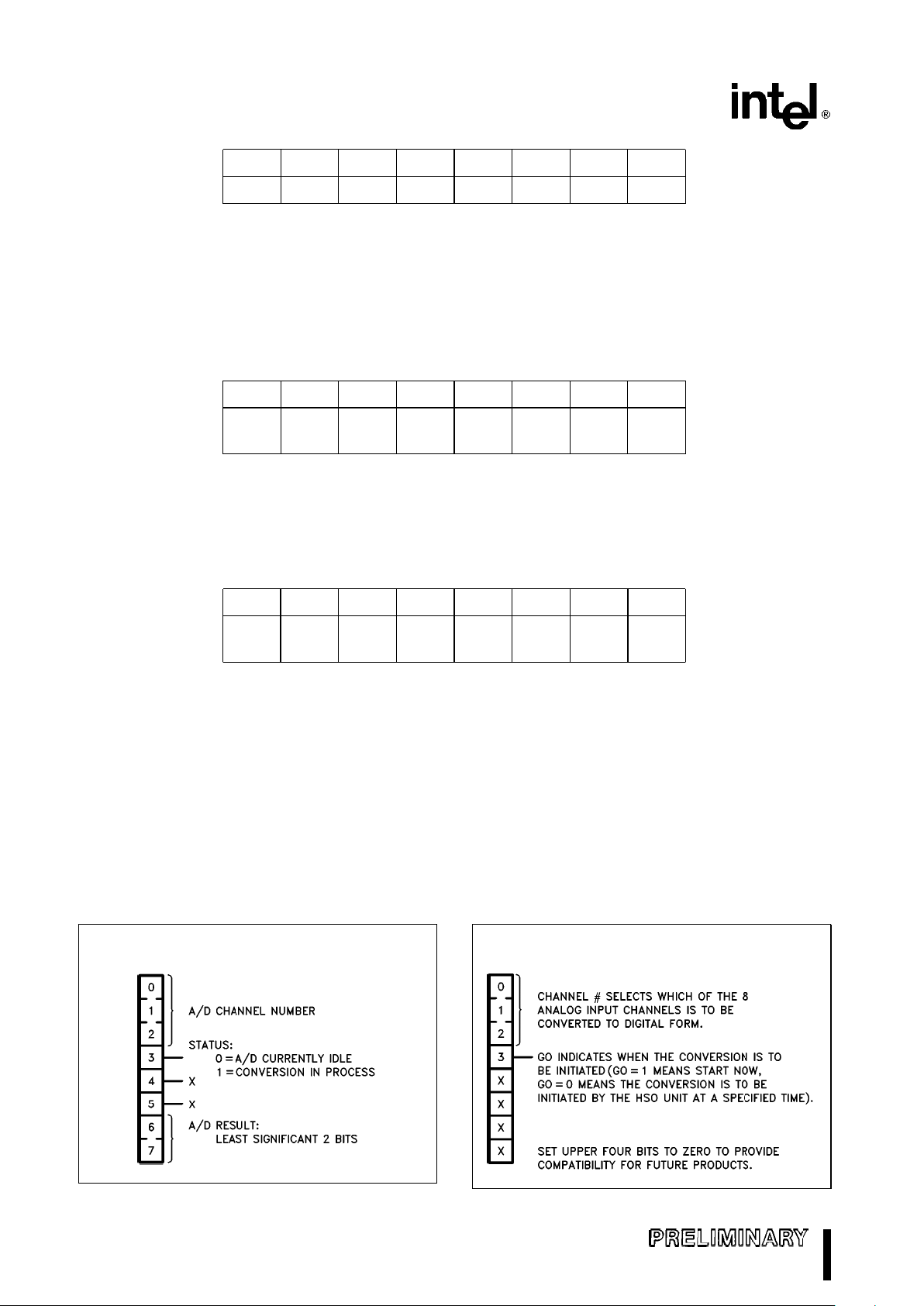
271089–4
A/D Command (02H)
271089–5
18
Page 19

M80C196KB
Chip Configuration (2018H)
271089–6
*Minor Change
HSIÐMode (03H)
271089–7
HSIÐStatus (06H)
271089–8
HSO Command (06H)
271089–9
*Minor Change
SPCON (11H)
271089–10
IOS0 (15H)
271089–11
19
Page 20

M80C196KB
IOC0 (15H)
271089–12
IOS1 (16H)
271089–13
IOC1 (16H)
271089–14
Port 2 Multiple Functions
Pin Func.
Alternative Control
Function Reg.
2.0 Output TXD (Serial Port IOC1.5
Transmit)
2.1 Input RXD (Serial Port SPCON.3
Receive)
2.3 Input T2CLK (Timer2 Clock IOC0.7
& Baud)
2.4 Input T2RST (Timer2 Reset) IOC0.5
2.5 Output PWM Output IOC1.0
2.6 QBD* Timer2 up/ IOC2.1
down select
2.7 QBD* Timer2 Capture N/A
*QBDeQuasi-bidirectional
Baud Rate Calculations
Asynchronous Modes 1, 2 and 3:
BaudÐReg
e
XTAL1
Baud Ratec16
b
1OR
T2CLK
Baud Ratec8
Synchronous Mode 0:
BaudÐReg
e
XTAL1
Baud Ratec2
b
1OR
T2CLK
Baud Rate
Baud Rates and Baud Register Values
Baud XTAL Frequency
Rate
8.0 MHz 10.0 MHz 12.0 MHz
300 1666b0.02 2082 0.02 2499 0.00
1200 416
b
0.08 520
b
0.03 624 0.00
2400 207 0.16 259 0.16 312
b
0.16
4800 103
b
0.16 129 0.16 155 0.16
9600 51
b
0.16 64 0.16 77 0.16
19.2K 25 0.16 32 1.40 38 0.16
Baud Register Value/% Error
A maximum baud rate of 750 Kbaud is available in
the asynchronous modes with 12 MHz on XTAL1.
The synchronous mode has a maximum rate of 3.0
Mbaud with a 12 MHz clock. Location 0EH is the
Baud Register. It is loaded sequentially in two bytes,
with the low byte being loaded first. This register
may not be loaded with zero in serial port Mode 0.
NOTE:
The maximum T2CLK rate is 3 MHz when used to
set the baud rate.
20
Page 21

M80C196KB
ELECTRICAL CHARACTERISTICS
Absolute Maximum Ratings*
Case Temperature
under Bias АААААААААААААААААА
b
55§Ctoa125§C
Storage Temperature АААААААААА
b
65§Ctoa150§C
Voltage On Any Pin to VSSААААААААb0.5V toa7.0V
Power DissipationАААААААААААААААААААААААААА1.5W
NOTICE: This data sheet contains preliminary information on new products in production. The specifications are subject to change without notice. Verify with
your local Intel Sales office that you have the latest
data sheet before finalizing a design.
*
WARNING: Stressing the device beyond the ‘‘Absolute
Maximum Ratings’’ may cause permanent damage.
These are stress ratings only. Operation beyond the
‘‘Operating Conditions’’ is not recommended and extended exposure beyond the ‘‘Operating Conditions’’
may affect device reliability.
OPERATING CONDITIONS
MIL-STD-883
Symbol Description Min Max Units
T
C
Case Temperature (Instant On)
b
55
a
125
§
C
V
CC
Digital Supply Voltage 4.50 5.50 V
V
REF
Analog Supply Voltage 4.50 5.50 V
f
OSC
Oscillator Frequency 3.5 12 MHz
Military Temperature (MTO)
Symbol Description Min Max Units
T
C
Case Temperature (Instant On)
b
55
a
125
§
C
V
CC
Digital Supply Voltage 4.50 5.50 V
V
REF
Analog Supply Voltage 4.50 5.50 V
f
OSC
Oscillator Frequency 3.5 12 MHz
NOTE:
ANGND and VSSshould be nominally at the same potential.
DC Characteristics (Over Specified Operating Conditions)
Symbol Description Min Max Units Comments
V
IL
Input Low Voltage
b
0.5 0.8 V
V
IH
Input High Voltage (Note 1) 0.2 V
CC
a
1.0 V
CC
V
V
IH1
Input High Voltage on XTAL 1 0.7 V
CC
V
CC
V
V
IH2
Input High Voltage on RESET 2.2 V
CC
V
V
OL
Output Low Voltage 0.3 V I
OL
e
200 mA
0.45 V I
OL
e
3.2 mA
1.5 V I
OL
e
7mA
V
OH
Output High Voltage V
CC
b
0.3 V I
OH
eb
200 mA
(Standard Outputs) (Note 2) V
CC
b
0.7 V I
OH
eb
3.2 mA
V
CC
b
1.5 V I
OH
eb
7mA
V
OH1
Output High Voltage V
CC
b
0.3 V I
OH
eb
10 mA
(Quasi-bidirectional Outputs) (Note 3) V
CC
b
0.7 V I
OH
eb
30 mA
V
CC
b
1.5 V I
OH
eb
60 mA
NOTES:
1. All pins except RESET and XTAL1.
2. Standard Outputs include AD0– 15, RD,WR, ALE, BHE, INST, HSO pins, PWM/P2.5, CLKOUT, RESET, Ports 3 and 4,
TXD/P2.0, and RXD (in serial mode 0). The V
OH
specification is not valid for RESET. Ports 3 and 4 are open-drain outputs.
3. QBD (Quasi-bidirectional) pins include Port 1, P2.6 and P2.7.
21
Page 22

M80C196KB
DC Characteristics (Over Specified Operating Conditions) (Continued)
Symbol Description Min Max Units Comments
I
LI
Input Leakage Current (Std. Inputs) (Note 4)
g
10 mA0
k
V
IN
k
V
CC
b
0.3V
I
LI1
Input Leakage Current ()
g
7mA0
k
V
IN
k
V
REF
I
TL
1 to 0 Transition Current (QBD Pins) (Note 3)
b
800 mAV
IN
e
2.0V
I
IL
Logical 0 Input Current (QBD Pins) (Note 3)
b
50 mAV
IN
e
0.45V
I
IL1
Logical 0 Input Current in Reset (Note 5)
b
850 mAV
IN
e
0.45 V
(ALE, RD
,WR, BHE, INST, P2.0)
I
CC
Active Mode Current in Reset 60 mA XTAL1e12 MHz
I
REF
A/D Converter Reference Current 5 mA
V
CC
e
V
PP
e
V
REF
e
5.5V
I
IDLE
Idle Mode Current 25 mA
I
CC1
Active Mode Current 30 mA XTAL1e3.5 MHz
I
PD
Powerdown Mode Current 50 mAV
CC
e
V
PP
e
V
REF
e
5.5V,
XTAL1
e
12 MHz
R
RST
Reset Pullup Resistor 6K 50K X
C
S
Pin Capacitance (Any Pin to VSS)10pFf
TEST
e
1.0 MHz
NOTES:
(Notes apply to all specifications)
2. Standard Outputs include AD0– 15, RD
,WR, ALE, BHE, INST, HSO pins, PWM/P2.5, CLKOUT, RESET, Ports 3 and 4,
TXD/P2.0, and RXD (in serial mode 0). The V
OH
specification is not valid for RESET. Ports 3 and 4 are open-drain outputs.
3. QBD (Quasi-bidirectional) pins include Port 1, P2.6 and P2.7.
4. Standard Inputs include HSI pins, EA
, READY, BUSWIDTH, NMI, RXD/P2.1, EXTINT/P2.2, T2CLK/P2.3, and T2RST/
P2.4.
5. Holding these pins below V
IH
in Reset may cause the part to enter test modes.
6. Maximum current per pin must be externally limited to the following values if V
OL
is held above 0.45V or VOHis held
below V
CC
b
0.7V:
I
OL
on Output pins: 10 mA
I
OH
on quasi-bidirectional pins: self limiting
I
OH
on Standard Output pins: 10 mA
7. Maximum current per bus pin (data and control) during normal operation is
g
3.2 mA.
8. During normal (non-transient) conditions the following total current limits apply:
Port 1, P2.6 I
OL
:29mA IOHis self limiting
HSO, P2.0, RXD, RESET
IOL:29mA IOH:26mA
P2.5, P2.7, WR
, BHE IOL:13mA IOH:11mA
AD0–AD15 I
OL
:52mA IOH:52mA
RD
, ALE, INST– CLKOUT IOL:13mA IOH:13mA
271089–16
Figure 4. ICCand I
IDLE
vs Frequency
22
Page 23

M80C196KB
AC Characteristics (Over Specified Operating Conditions)
Test Conditions: Capacitive load on all pins
e
100 pF, Rise and fall timese10 ns, f
OSC
e
12 MHz
The system must meet these specifications to work with the M80C196KB:
Symbol Description Min Max Units Notes
T
AVYV
Address Valid to READY Setup 2T
OSC
b
85 ns
T
LLYV
ALE Low to READY Setup
M80C196KB T
OSC
b
75 ns
T
YLYH
Non READY Time No upper limit ns
T
CLYX
READY Hold after CLKOUT Low 0 T
OSC
b
30 ns (Note 1)
T
LLYX
READY Hold after ALE Low T
OSC
b
15 2T
OSC
b
40 ns (Note 1)
T
AVGV
Address Valid to Buswidth Setup 2T
OSC
b
85 ns
T
LLGV
ALE Low to Buswidth Setup T
OSC
b
70 ns
T
CLGX
Buswidth Hold after CLKOUT Low 0 ns
T
AVDV
Address Valid to Input Data Valid
M80C196KB 3T
OSC
b
67 ns
T
RLDV
RD Active to Input Data Valid
M80C196KB T
OSC
b
23 ns
T
CLDV
CLKOUT Low to Input Data Valid T
OSC
b
50 ns
T
RHDZ
End of RD to Input Data Float T
OSC
b
20 ns
T
RXDX
Data Hold after RD Inactive 0 ns
NOTE:
1. If max is exceeded, additional wait states will occur.
23
Page 24

M80C196KB
AC Characteristics (Over Specified Operating Conditions) (Continued)
Test Conditions: Capacitive load on all pins
e
100 pF, Rise and fall timese10 ns, f
OSC
e
12 MHz
The M80C196KB will meet these specifications:
Symbol Description Min Max Units Notes
F
XTAL
Frequency on XTAL
1
M80C196KB 3.5 12 MHz
T
OSC
I/F
XTAL
M80C196KB 83 286 ns
T
XHCH
XTAL1 High to CLKOUT High or Low 20 110 ns
T
CLCL
CLKOUT Cycle Time 2T
OSC
ns
T
CHCL
CLKOUT High Period T
OSC
b
10 T
OSC
a
10 ns
T
CLLH
CLKOUT Falling Edge to ALE Rising
b
10 10 ns
T
LLCH
ALE Falling Edge to CLKOUT Rising
b
15 15 ns
T
LHLH
ALE Cycle Time 4T
OSC
ns
T
LHLL
ALE High Period T
OSC
b
12 T
OSC
a
12 ns
T
AVLL
Address Setup to ALE Falling Edge T
OSC
b
20 ns
T
LLAX
Address Hold after ALE Falling Edge T
OSC
b
40 ns
T
LLRL
ALE Falling Edge to RD Falling Edge T
OSC
b
40 ns
T
RLCL
RD Low to CLKOUT Falling Edge 4 25 ns
T
RLRH
RD Low Period T
OSC
b
5ns
T
RHLH
RD Rising Edge to ALE Rising Edge T
OSC
T
OSC
a
25 ns (Note 2)
T
RLAZ
RD Low to Address Float 10 ns
T
LLWL
ALE Falling Edge to WR Falling Edge T
OSC
b
10 ns
T
CLWL
CLKOUT Low to WR Falling Edge 0 25 ns
T
QVWH
Data Stable to WR Rising Edge
M80C196KB T
OSC
b
23 ns
T
CHWH
CLKOUT High to WR Rising Edge
b
515ns
T
WLWH
WR Low Period T
OSC
b
30 ns
T
WHQX
Data Hold after WR Rising Edge T
OSC
b
15 ns
T
WHLH
WR Rising Edge to ALE Rising Edge T
OSC
b
15 T
OSC
a
10 ns (Note 2)
T
WHBX
BHE, INST HOLD after WR Rising Edge T
OSC
b
15 ns
NOTE:
2. Assuming back-to-back bus cycles.
24
Page 25

M80C196KB
System Bus Timings
271089–17
271089–18
25
Page 26

M80C196KB
EXTERNAL CLOCK DRIVE
Symbol Parameter Min Max Units
1/T
XLXL
Oscillator Frequency
M80C196KB 3.5 12.0 MHz
T
XLXL
Oscillator Period
M80C196KB 83 286 ns
T
XHXX
High Time 32 ns
T
XLXX
Low Time 32 ns
T
XLXH
Rise Time 10 ns
T
XHXL
Fall Time 10 ns
EXTERNAL CLOCK DRIVE WAVEFORMS
271089–19
AC TESTING INPUT, OUTPUT WAVEFORMS
271089–20
AC Testing inputs are driven at 2.4V for a Logic ‘‘1’’ and 0.45V for
a Logic ‘‘0’’ Timing measurements are made at 2.0V for a Logic
‘‘1’’ and 0.8V for a Logic ‘‘0’’.
FLOAT WAVEFORMS
271089–21
For Timing Purposes a Port Pin is no Longer Floating when a
100 mV change from Load Voltage Occurs and Begins to Float
when a 100 mV change from the Loaded V
OH/VOL
Level occurs
I
OL/IOH
e
g
15 mA.
EXPLANATION OF AC SYMBOLS
Each symbol is two pairs of letters prefixed by ‘‘T’’ for time. The characters in a pair indicate a signal and its
condition, respectively. Symbols represent the time between the two signal/condition points.
Conditions:
H - High
L - Low
V - Valid
X - No Longer Valid
Z - Floating
Signals:
A - Address
B - BHE
C - CLKOUT
D - DATA
G - Buswidth
L - ALE/ADV
R-RD
W-WR/WRH/WRL
X - XTAL1
Y - READY
26
Page 27

M80C196KB
AC CHARACTERISTICSÐSERIAL PORTÐSHIFT REGISTER MODE
SERIAL PORT TIMINGÐSHIFT REGISTER MODE
Symbol Parameter Min Max Units
T
XLXL
Serial Port Clock Period (BRRt8002H) 6 T
OSC
ns
T
XLXH
Serial Port Clock Falling Edge 4 T
OSC
b
50 4 T
OSC
a
50 ns
to Rising Edge (BRR
t
8002H)
T
XLXL
Serial Port Clock Period (BRRe8001H) 4 T
OSC
ns
T
XLXH
Serial Port Clock Falling Edge 2 T
OSC
b
50 2 T
OSC
a
50 ns
to Rising Edge (BRR
e
8001H)
T
QVXH
Output Data Setup to Clock Rising Edge 2 T
OSC
b
50 ns
T
XHQX
Output Data Hold after Clock Rising Edge 2 T
OSC
b
50 ns
T
XHQV
Next Output Data Valid after Clock Rising Edge 2 T
OSC
a
50 ns
T
DVXH
Input Data Setup to Clock Rising Edge T
OSC
a
50 ns
T
XHDX
Input Data Hold after Clock Rising Edge 0 ns
T
XHQZ
Last Clock Rising to Output Float T
OSC
ns
WAVEFORMÐSERIAL PORTÐSHIFT REGISTER MODE
SERIAL PORT WAVEFORMÐSHIFT REGISTER MODE
271089–22
27
Page 28

M80C196KB
A TO D CHARACTERISTICS
There are two modes of A/D operation: with or without clock prescaler. The speed of the A/D converter
can be adjusted by setting a clock prescaler on or
off. At high frequencies more time is needed for the
comparator to settle. The maximum frequency with
the clock prescaler disabled is 8 MHz. The conversion times with the prescaler turned on or off is
shown in the table below.
The converter is ratiometric, so the absolute
accuracy is directly dependent on the accuracy and
stability of V
REF.VREF
must be close to VCCsince it
supplies both the resistor ladder and the digital section of the converter.
A/D CONVERTER SPECIFICATIONS
The specifications given below assume adherence
to the Operating Conditions section of this data
sheet. Testing is performed in Mode 2 with V
REF
e
5.12V and 12 MHz on XTAL1.
Clock Prescaler On Clock Prescaler Off
IOC2.4
e
0 IOC2.4e1
Mode 0 –158 States Mode 2 –91 States
26.33 ms
@
12 MHz 22.75 ms@8 MHz
A/D CHARACTERISTICS (Over Specified Operating Conditions)
Parameter Typical*(1) Minimum Maximum Units** Notes
Resolution 256 1024 Levels
10 Bits
Absolute Error 0
g
4 LSBs
Full Scale Error
b
0.5
g
0.5 LSBs
Zero Offset Error
g
0.5 LSBs
Non-Linearity 0
g
4 LSBs
Differential Non-Linearity 0
g
2 LSBs
Channel-to-Channel Matching 0
g
1 LSBs
Repeatability
g
0.25 LSBs
Temperature Coefficients:
Offset 0.009 LSB/
§
C
Full Scale 0.009 LSB/
§
C
Differential Non-Linearity 0.009 LSB/
§
C
Off Isolation
b
60 dB 2, 3
Feedthrough
b
60 dB 2
VCCPower Supply Rejection
b
60 dB 2
Input Resistance 750 1.2K X
DC Input Leakage 0 3.0 mA
Sample Time Slow Mode 15 States 4
Fast Mode 8 States 4
Input Capacitance 3 pF
NOTES:
*An ‘‘LSB’’, as used here, has a value of approximately 5 mV.
1. These values are expected for most parts at 25
§
C but are not tested or guaranteed.
2. DC to 100 KHz.
3. Multiplexer Break-Before-Make Guaranteed.
4. One state
e
167 ns at 12 MHz, 250 ns at 8 MHz.
28
Page 29

M80C196KB
A/D GLOSSARY OF TERMS
ABSOLUTE ERRORÐThe maximum difference be-
tween corresponding actual and ideal code transitions. Absolute Error accounts for all deviations of
an actual converter from an ideal converter.
ACTUAL CHARACTERISTICÐThe characteristic
of an actual converter. The characteristic of a given
converter may vary over temperature, supply voltage, and frequency conditions. An actual characteristic rarely has ideal first and last transition locations
or ideal code widths. It may even vary over multiple
conversions under the same conditions.
BREAK-BEFORE-MAKEÐThe property of multiplexer which guarantees that a previously selected
channel will be deselected before a new channel is
selected (e.g., the converter will not short inputs together).
CHANNEL-TO-CHANNEL MATCHINGÐThe difference between corresponding code transitions of actual characteristics taken from different channels under the same temperature, voltage and frequency
conditions.
CHARACTERISTICÐA graph of input voltage versus the resultant output code for an A/D converter.
It describes the transfer function of the A/D converter.
CODEÐThe digital value output by the converter.
CODE TRANSITIONÐThe point at which the con-
verter changes from an output code of Q, to a code
of Q
a
1. The input voltage corresponding to a code
transition is defined to be that voltage which is
equally likely to produce either of two adjacent
codes.
CODE WIDTHÐThe voltage corresponding to the
difference between two adjacent code transitions.
DC INPUT LEAKAGEÐLeakage current to ground
from an analog input pin.
DIFFERENTIAL NON-LINEARITYÐThe difference
between the ideal and actual code widths of the terminal based characteristic.
FEEDTHROUGHÐAttenuation of a voltage applied
on the selected channel of the A/D Converter after
the sample window closes.
FULL SCALE ERRORÐThe difference between the
expected and actual input voltage corresponding to
the full scale code transition.
IDEAL CHARACTERISTICÐA characteristic with
its first code transition at V
IN
e
0.5 LSB, its last
code transition at V
IN
e
(V
REF
b
1.5 LSB) and all
code widths equal to one LSB.
INPUT RESISTANCEÐThe effective series resistance from the analog input pin to the sample capacitor.
LSBÐLeast Significant Bit: The voltage corresponding to the full scale voltage divided by 2
n
,
where n is the number of bits of resolution of the
converter. For an 8-bit converter with a reference
voltage of 5.12V, one LSB is 20 mV. Note that this is
different than digital LSBs, since an uncertainty of
two LSB, when referring to an A/D converter, equals
40 mV. (This has been confused with an uncertainty
of two digital bits, which would mean four counts, or
80 mV.)
NON-LINEARITYÐThe maximum deviation of code
transitions of the terminal based characteristic from
the corresponding code transitions of the ideal characteristic.
OFF-ISOLATIONÐAttenuation of a voltage applied
on a deselected channel of the A/D converter. (Also
referred to as Crosstalk.)
REPEATABILITYÐThe difference between corresponding code transitions from different actual characteristics taken from the same converter on the
same channel at the same temperature, voltage and
frequency conditions.
RESOLUTIONÐThe number of input voltage levels
that the converter can unambiguously distinguish
between. Also defines the number of useful bits of
information which the converter can return.
SAMPLE TIMEÐBegins when the sample capacitor
is attached to a selected channel and ends when
the sample capacitor is disconnected from the selected channel.
TEMPERATURE COEFFICIENTSÐChange in the
stated variable per degree centigrade temperature
change. Temperature coefficients are added to the
typical values of a specification to see the effect of
temperature drift.
TERMINAL BASED CHARACTERISTICÐAn actual
characteristic which has been rotated and translated
to remove zero offset and full scale error.
V
CC
REJECTIONÐAttenuation of noise on the V
CC
line to the A/D converter.
ZERO OFFSETÐThe difference between the expected and actual input voltage corresponding to
the first code transition.
29
Page 30

M80C196KB
M80C196KB FUNCTIONAL
DEVIATIONS
The M80C196KB has the following problems.
1. The DJNZW instruction is guaranteed to be functional. The DJNZ (byte instruction) work around is
no longer needed.
2. The serial port only tolerates a
a
1.25%,b7.5%
baud rate error between Transmitter and Receiver. If the serial port fails on the receiver, increase
the baud rate.
3. The HSI unit has two errata: one dealing with resolution and the other with first entries into the
FIFO.
The HSI resolution is 9 states instead of 8 states.
Events on the same line may be lost if they occur
faster than once every 9 state times.
There is a mismatch between the 9 state time HSI
resolution and the 8 state time timer. This causes
one time value to be unused every 9 timer counts.
Events may receive a time-tag one count later
than expected because of this ‘‘skipped’’ time value.
If the first two events into an empty FIFO (not
including the Holding Register) occur in the same
internal phase, both are recorded with one timetag. Otherwise, if the second event occurs within
9 states after the first, its time-tag is one count
later than the first’s. If this is the ‘‘skipped’’ time
value, the second event’s time-tag is 2 counts later than the first’s.
If the FIFO and Holding Register are empty, the
first event will transfer into the Holding Register
after 8 state times, leaving the FIFO empty again.
If the second event occurs after this time, it will
act as a new first event into an empty FIFO.
4. The serial port Framing Error flag that failed to indicate an error if the bit preceding the stop bit is a
1 has been fixed.
CONVERTING FROM OTHER M8097
FAMILY PRODUCTS TO THE
M80C196KB
The following list of suggestions for designing an
M809XBH system will yield a design that is easily
converted to the M80C196KB.
1. Do not base critical timing loops on instruction or
peripheral execution times.
2. Use equate statements to set all timing parameters, including the baud rate.
3. Do not base hardware timings on CLKOUT or
XTAL1. The timings of the M80C196KB are different than those of the M8X9XBH, but they will
function with standard ROM/EPROM/Peripheral
type memory systems.
4. Make sure all inputs are tied high or low and not
left floating.
5. Indexed and indirect operations relative to the
stack pointer (SP) work differently on the
M80C196KB than on the M8097. On the M8097,
the address is calculated based on the un-updated version of the stack pointer. The M80C196KB
uses the updated version. The offset for
PUSH[SP], POP[SP], PUSH nn[SP]and POP
nn[SP]instructions may need to be changed by a
count of 2.
30
 Loading...