

Intel Corporation MD80C287 Datasheet
November 1991 Order Number: 271092-005
M80C287
80-BIT CHMOS III NUMERIC PROCESSOR EXTENSION
Military
Y
High Performance 80-Bit Internal
Architecture
Y
Implements ANSI/IEEE Standard 7541985 for Binary Floating-Point
Arithmetic
Y
Implements Extended M387 Numerics
Coprocessor Instruction Set
Y
Two to Three Times M8087/M80287
Performance at Equivalent Clock Speed
Y
Low Power Consumption
Y
Upward Object-Code Compatible from
M8087 and M80287
Y
Interfaces with M80286 and M80C286
CPUs
Y
Expands CPU’s Data Types to Include
32-, 64-, 80-Bit Floating Point, 32-, 64Bit Integers and 18-Digit BCD Operands
Y
Directly Extends CPU’s Instruction Set
to Trigonometric, Logarithmic,
Exponential, and Arithmetic
Instructions for All Data Types
Y
Full-Range Transcendental Operations
for SINE, COSINE, TANGENT.
ARCTANGENT and LOGARITHM
Y
Built-In Exception Handling
Y
Operates in Both Real and Protected
Mode Systems
Y
Eight 80-Bit Numeric Registers, Usable
as Individually Addressable General
Registers or as a Register Stack
Y
Available in 40-pin CERDIP
(See Packaging Outlines and Dimensions, orderÝ231369)
Y
Military Temperature Range:
b
55§Ctoa125§C(TC)
The Intel M80C287 is a high-performance numerics processor extension that extends the architecture of the
M80C286 CPU with floating point, extended integer, and BCD data types. A computing system that includes
the M80C287 fully conforms to the IEEE Floating Point Standard. Using a numerics oriented architecture, the
M80C287 adds over seventy mnemonics to the instruction set of the M80C286 CPU, making a complete
solution for high-performance numerics processing. The M80C287 is implemented with 1.5 micron, high-speed
CHMOS III technology and packaged in a 40-pin CERDIP. The M80C287 is upward object-code compatible
from the M80287 and M8087 numerics coprocessors. With proper socket design, either an M80287 or an
M80C287 can use the same socket.
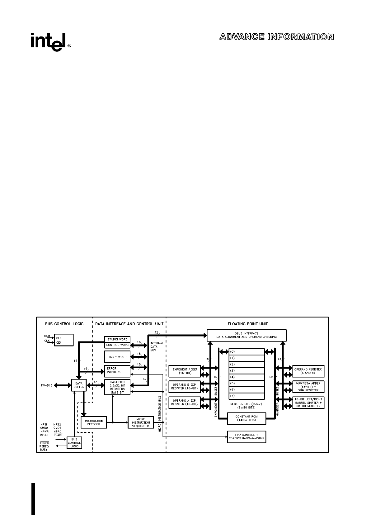
271092–1
Figure 1. M80C287 Block Diagram
M80C287
M80C287 Data Registers
79 78 64 63 0
R0 Sign Exponent Significand
R1
R2
R3
R4
R5
R6
R7
15 0 31 15 0
Control Register Instruction Pointer
Status Register Data Pointer
Tag Word
Figure 2. M80C287 Register Set
FUNCTIONAL DESCRIPTION
The M80C287 Numeric Processor Extension (NPX)
provides arithmetic instructions for a variety of numeric data types. It also executes numerous built-in
transcendental functions (e.g. tangent, sine, cosine,
and log functions). The M80C287 effectively extends the register and instruction set of the CPU for
existing data types and adds several new data types
as well. Figure 2 shows the additional registers visible to programs in a system that includes the
M80C287. Essentially, the M80C287 can be treated
as an additional resource or an extension to the
M80C286 CPU. The M80C286 CPU together with an
M80C287 NPX can be used as a single unified system.
The M80C287 has two operating modes. After reset,
the M80C287 is in the real-address mode. It can be
placed into protected mode by executing the
FSETPM instruction. It can be switched back to realaddress mode by executing the FRSTPM instruction
(note that this feature is useful only with CPU’s that
can also switch back to real-address mode). These
instructions control the format of the administrative
instructions FLDENV, FSTENV, FRSTOR, and
FSAVE. Regardless of operating mode, all references to memory for numerics data or status information are performed by the M80C286 CPU, and
therefore obey the memory-management and protection rules of the M80C286 CPU.
In real-address mode, a system that includes the
M80C287 is completely upward compatible with
software for the M8086/M8087 and for M80286/
M80287 real-address mode.
In protected mode, a system that includes the
M80C287 is completely upward compatible with
software for M80286/M80287 protected mode systems.
The only differences of operation that may appear
when M8086/M8087 programs are ported to a protected-mode M80C287 system are in the format of
operands for the administrative instructions
FLDENV, FSTENV, FRSTOR, and FSAVE. These instructions are normally used only by exception handlers and operating systems, not by applications
programs.
PROGRAMMING INTERFACE
The M80C287 adds to the CPU additional data
types, registers, instructions, and interrupts specifically designed to facilitate high-speed numerics processing. To use the M80C287 requires no special
programming tools, because all new instructions and
data types are directly supported by the assembler
and compilers for high-level languages. All 8086/
8088 development tools that support the M8087 can
also be used to develop software for the M80C286/
M80C287 in real-address mode. All M80286 development tools that support the M80287 can also be
used to develop software for the M80C286/
M80C287. The M80C287 supports all M387 NPX instructions, producing the same binary results.
All communication between the M80C286 CPU and
the M80C287 is transparent to applications software. The M80C286 CPU automatically controls the
M80C287 whenever a numerics instruction is executed. All physical memory and virtual memory of
the M80C286 CPU are available for storage of the
instructions and operands of programs that use the
M80C287. All memory addressing modes are available for addressing numerics operands.
The instructions that the M80C287 adds to the instruction set are listed at the end of this data sheet.
2

M80C287
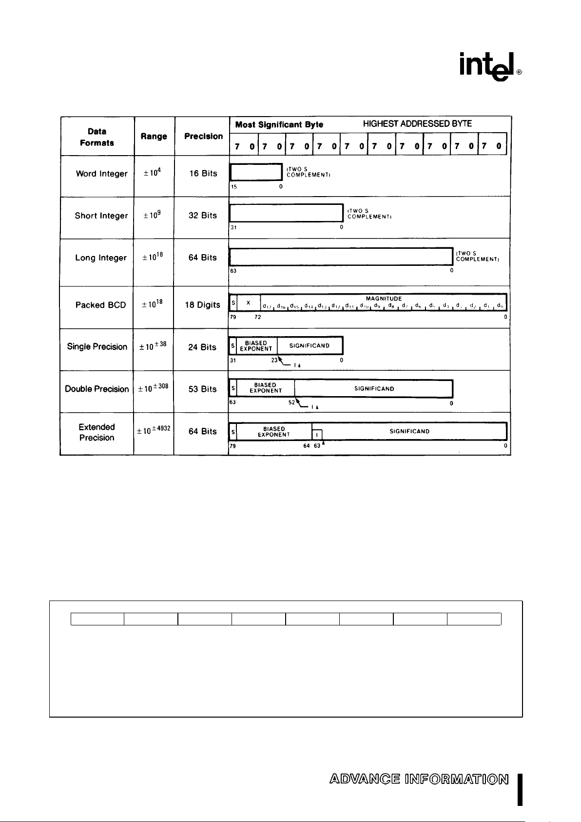
Data Types
Table 1 lists the seven data types that the M80C287
supports and presents the format for each type. Operands are stored in memory with the least significant digit at the lowest memory address. Programs
retrieve these values by generating the lowest address. For maximum system performance, all operands should start at physical-memory addresses
that correspond to the word size of the CPU; operands may begin at any other addresses, but will require extra memory cycles to access the entire operand.
Internally, the M80C287 holds all numbers in the extended-precision real format. Instructions that load
operands from memory automatically convert operands represented in memory as 16-, 32-, or 64-bit
integers, 32- or 64-bit floating-point numbers, or 18digit packed BCD numbers into extended-precision
real format. Instructions that store operands in memory perform the inverse type conversion.
Numeric Operands
A typical NPX instruction accepts one or two operands and produces one (or sometimes two) results.
In two-operand instructions, one operand is the contents of an NPX register, while the other may be a
memory location. The operands of some instructions
are predefined; for example, FSQRT always takes
the square root of the number in the top stack element.
Register Set
Figure 2 shows the M80C287 register set. When an
M80C287 is present in a system, programmers may
use these registers in addition to the registers normally available on the CPU.
DATA REGISTERS
M80C287 computations use the M80C287’s data
registers. These eight 80-bit registers provide the
equivalent capacity of 20 32-bit registers. Each of
the eight data registers in the M80C287 is 80 bits
wide and is divided into ‘‘fields’’ corresponding to
the NPX’s extended-precision real data type.
The M80C287 register set can be accessed either
as a stack, with instructions operating on the top one
or two stack elements, or as individually addressable
registers. The TOP field in the status word identifies
the current top-of-stack register. A ‘‘push’’ operation
decrements TOP by one and loads a value into the
new top register. A ‘‘pop’’ operation stores the value
from the current top register and then increments
TOP by one. The M80C287 register stack grows
‘‘down’’ toward lower-addressed registers.
Instructions may address the data registers either
implicitly or explicitly. Many instructions operate on
the register at the TOP of the stack. These instructions implicitly address the register at which TOP
points. Other instructions allow the programmer to
explicitly specify which register to use. This explicit
register addressing is also relative to TOP.
TAG WORD
The tag word marks the content of each numeric
data register, as Figure 3 shows. Each two-bit tag
represents one of the eight data registers. The principal function of the tag word is to optimize the
NPX’s performance and stack handling by making it
possible to distinguish between empty and nonempty register locations. It also enables exception handlers to identify special values (e.g. NaNs or denormals) in the contents of a stack location without the
need to perform complex decoding of the actual
data.
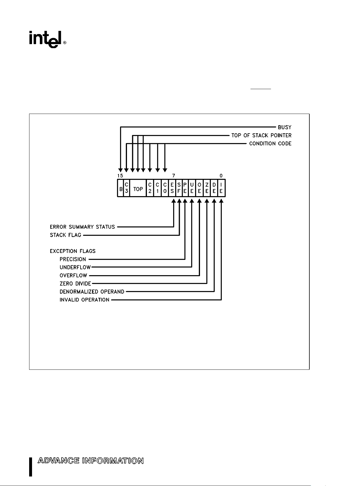
STATUS WORD
The 16-bit status word (in the status register) shown
in Figure 4 reflects the overall state of the M80C287.
It may be read and inspected by programs.
Bit 15, the B-bit (busy bit) is included for M8087
compatibility only. It always has the same value as
the ES bit (bit 7 of the status word); it does not
indicate the status of the BUSY
output of M80C287.
Bits 13– 11 (TOP) point to the M80C287 register that
is the current top-of-stack.
The four numeric condition code bits (C
3–C0
) are
similar to the flags in a CPU; instructions that perform arithmetic operations update these bits to reflect the outcome. The effects of these instructions
on the condition code are summarized in Tables 2
through 5.
Bit 7 is the error summary (ES) status bit. This bit is
set if any unmasked exception bit is set; it is clear
otherwise. If this bit is set, the ERROR
signal is as-
serted.
Bit 6 is the stack flag (SF). This bit is used to distinguish invalid operations due to stack overflow or underflow from other kinds of invalid operations. When
SF is set, bit 9 (C
1
) distinguishes between stack
overflow (C
1
e
1) and underflow (C
1
e
0).
3
M80C287
Table 1. M80C287 Data Type Representation in Memory
271092–2
NOTES:
1. S
e
Sign bit (0epositive, 1enegative)
2. d
n
e
Decimal digit (two per byte)
3. X
e
Bits have no significance: M80C287 ignores when loading, zeroes when storing
4.
U
e
Position of implicit binary point
5. I
e
Integer bit of significand; stored in temporary real, implicit in single and double precision
6. Exponent Bias (normalized values):
Single: 127 (7FH)
Double: 1023 (3FFH)
Extended Real: 16383 (3FFFH)
7. Packed BCD: (
b
1)S(D17...D0)
8. Real: (
b
1)S(2
E-BIAS
)(F0F1...)
15 0
TAG (7) TAG (6) TAG (5) TAG (4) TAG (3) TAG (2) TAG (1) TAG (0)
NOTE:
The index i of tag(i) is not top-relative. A program typically uses the ‘‘top’’ field of Status Word to determine which tag(i)
field refers to logical top of stack.
TAG VALUES:
00
e
Valid
01eZero
10
e
QNaN, SNaN, Infinity, Denormal and Unsupported Formats
11
e
Empty
Figure 3. M80C287 Tag Word
4
M80C287
Figure 4 shows the six exception flags in bits 5– 0 of
the status word. Bits 5 –0 are set to indicate that the
M80C287 has detected an exception while executing an instruction. A later section entitled ‘‘Exception
Handling’’ explains how they are set and used.
Note that when a new value is loaded into the status
word by the FLDENV or FRSTOR instruction, the
value of ES (bit 7) and its reflection in the B-bit (bit
15) are not derived from the values loaded from
memory but rather are dependent upon the values of
the exception flags (bits 5 – 0) in the status word and
their corresponding masks in the control word. If ES
is set in such a case, the ERROR
output of the
M80C287 is activated immediately.
271092–3
ES is set if any unmasked exception bit is set; cleared otherwise.
See Table 2.2 for interpretation of condition code.
TOP Values:
000
e
Register 0 is Top of Stack
001
e
Register 1 is Top of Stack
#
#
#
111eRegister 7 is Top of Stack
For definitions of exceptions, refer to the section entitled ‘‘Exception Handling.’’
Figure 4. Status Word
5
M80C287
Table 2. Condition Code Interpretation
Instruction C0 (S) C3 (Z) C1 (A) C2 (C)
FPREM, FPREM1 Three Least Significant Bits
Reduction
(See Table 3) of Quotient
0
e
Complete
Q2 Q0 Q1
1
e
Incomplete
or O/U
FCOM, FCOMP,
FCOMPP, FTST,
Result of Comparison Zero Operand is Not Comparable
FUCOM, FUCOMP,
(See Table 2.4) or O/U
(Table 2.4)
FUCOMPP, FICOM,
FICOMP
FXAM Operand Class Sign Operand Class
(See Table 2.5) or O/U
(Table 2.5)
FCHS, FABS, FXCH,
FINCTOP, FDECTOP,
Constant Loads,
UNDEFINED
Zero
UNDEFINED
FXTRACT, FLD, or O/U
FILD, FBLD,
FSTP (Ext Real)
FIST, FBSTP,
FRNDINT, FST
FSTP, FADD, FMUL,
FDIV, FDIVR,
UNDEFINED
Roundup
UNDEFINED
FSUB, FSUBR, or O/U
FSCALE, FSQRT,
FPATAN, F2XM1,
FYL2X, FYL2XP1
FPTAN, FSIN, Roundup
Reduction
FCOS, FSINCOS
UNDEFINED
or O/U
0eComplete
Undefined
1
e
Incomplete
if C2e1
FLDENV, FRSTOR Each Bit Loaded from Memory
FLDCW, FSTENV,
FSTCW, FSTSW,
UNDEFINED
FCLEX, FINIT,
FSAVE
O/U When both IE and SF bits of status word are set, indicating a stack exception, this bit distinguishes between
stack overflow (C1
e
1) and underflow (C1e0).
Reduction If FPREM or FPREM1 produces a remainder that is less than the modulus, reduction is complete. When
reduction is incomplete the value at the top of the stack is a partial remainder, which can be used as input to
further reduction. For FPTAN, FSIN, FCOS, and FSINCOS, the reduction bit is set if the operand at the top of
the stack is too large. In this case the original operand remains at the top of the stack.
Roundup When the PE bit of the status word is set, this bit indicates whether one was added to the least significant bit of
the result during the last rounding.
UNDEFINED Do not rely on finding any specific value in these bits.
6
M80C287
Table 3. Condition Code Interpretation after FPREM and FPREM1 Instructions
Condition Code Interpretation after
C2 C3 C1 C0
FPREM and FPREM1
1XXXIncomplete Reduction: Further iteration required for complete
reduction.
Q1 Q0 Q2 Q MOD 8 Complete Reduction: C0, C3, C1 contain three
least significant bits of quotient.
000 0
010 1
100 2
0
110 3
001 4
011 5
101 6
111 7
Table 4. Condition Code
Resulting from Comparison
Order C3 C2 C0
TOPlOperand 0 0 0
TOP
k
Operand 0 0 1
TOP
e
Operand 1 0 0
Unordered 1 1 1
Table 5. Condition Code
Defining Operand Class
C3 C2 C1 C0 Value at TOP
0000
a
Unsupported
0001
a
NaN
0010
b
Unsupported
0011
b
Nan
0100
a
Normal
0101
a
Infinity
0110
b
Normal
0111
b
Infinity
1000
a
0
1001
a
Empty
1010
b
0
1011
b
Empty
1100
a
Denormal
1110
b
Denormal
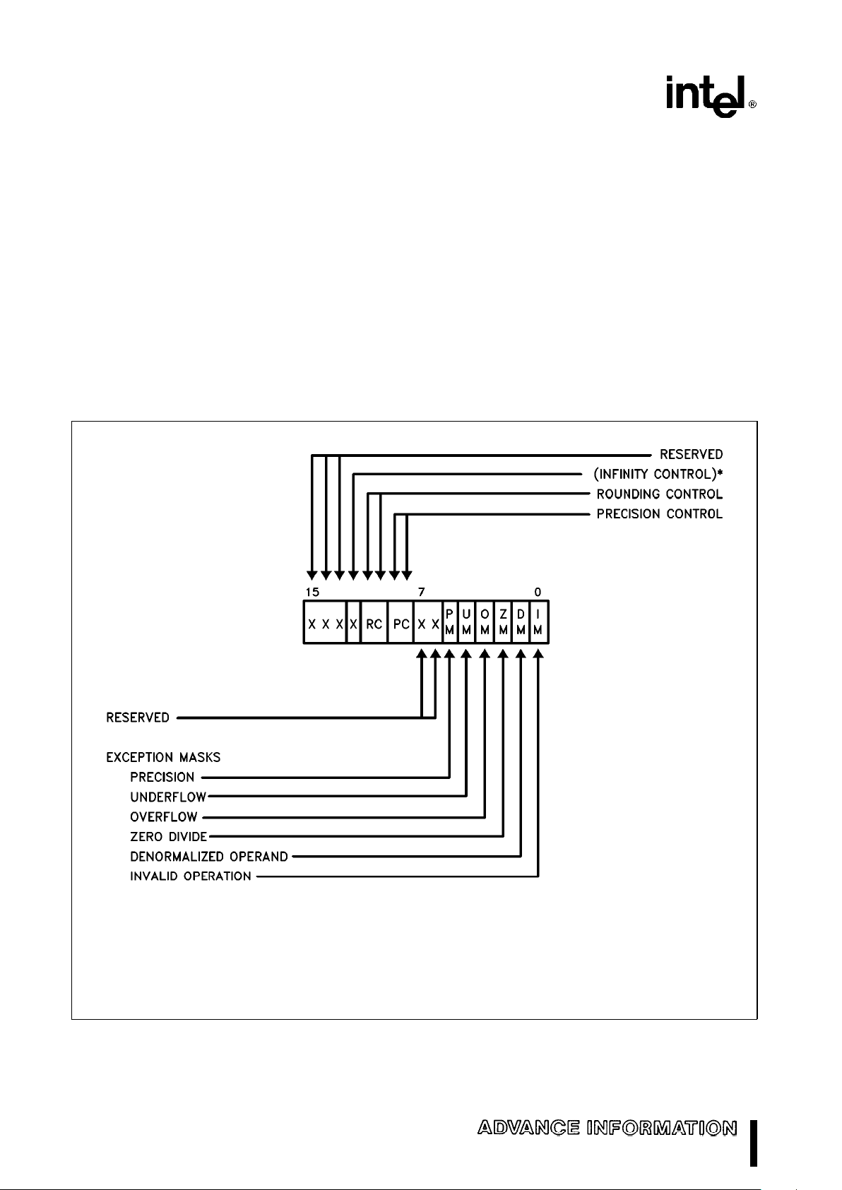
CONTROL WORD
The NPX provides several processing options that
are selected by loading a control word from memory
into the control register. Figure 5 shows the format
and encoding of fields in the control word.
The low-order byte of this control word configures
exception masking. Bits 5 –0 of the control word
contain individual masks for each of the six exceptions that the M80C287 recognizes.
The high-order byte of the control word configures
the M80C287 operating mode, including precision,
rounding, and infinity control.
#
The ‘‘infinity control bit’’ (bit 12) is not meaningful
to the M80C287, and programs must ignore its
value. To maintain compatibility with the M8087
and M80287, this bit can be programmed; however, regardless of its value, the M80C287 always
treats infinity in the affine sense (
b%ka %
).
This bit is initialized to zero both after a hardware
reset and after the FINIT instruction.
#
The rounding control (RC) bits (bits 11 – 10) provide for directed rounding and true chop, as well
as the unbiased round to nearest even mode
specified in the IEEE standard. Rounding control
affects only those instructions that perform
rounding at the end of the operation (and thus
can generate a precision exception); namely,
FST, FSTP, FIST, all arithmetic instructions (except FPREM, FPREM1, FXTRACT, FABS, and
FCHS), and all transcendental instructions.
#
The precision control (PC) bits (bits 9– 8) can be
used to set the M80C287 internal operating precision of the significand at less than the default of
64 bits (extended precision). This can be useful in
providing compatibility with early generation arithmetic processors of smaller precision. PC affects
only the instructions ADD, SUB, DIV, MUL, and
SQRT. For all other instructions, either the precision is determined by the opcode or extended
precision is used.
7
M80C287
INSTRUCTION AND DATA POINTERS
Because the NPX operates in parallel with the CPU,
any exceptions detected by the NPX may be reported after the CPU has executed the ESC instruction
which caused it. To allow identification of the failing
numeric instruction, the M80C287 contains registers
that aid in diagnosis. These registers supply the opcode of the failing numeric instruction, the address
of the instruction, and the address of its numeric
memory operand (if appropriate).
The instruction and data pointers are provided for
user-written exception handlers. Whenever the
M80C287 executes a new ESC instruction, it saves
the address of the instruction (including any prefixes
that may be present), the address of the operand (if
present), and the opcode. CPUs with 32-bit internal
architectures contain 32-bit versions of these registers and do not use the contents of the NPX registers. This difference is not apparent to programmers,
however.
The instruction and data pointers appear in one of
four formats depending on the operating mode of
the system (protected mode or real-address mode)
and (for CPUs with 32-bit internal architectures) depending on the operand-size attribute in effect (32bit operand or 16-bit operand). (See Figures 6 and 7)
The ESC instructions FLDENV, FSTENV, FSAVE,
and FRSTOR are used to transfer these values between the registers and memory. Note that the value
of the data pointer is
undefined
if the prior ESC in-
struction did not have a memory operand.
271092–4
Precision Control
00–24 bits (single precision)
01–(reserved)
10–53 bits (double precision)
11–64 bits (extended precision)
Rounding Control
00–Round to nearest or even
01–Round down (toward
b%
)
10–Round up (toward
a %
)
11–Chop (truncate toward zero)
*The ‘‘infinity control’’ bit is not meaningful to the M80C287. To maintain compatibility with the M80287, this bit can be
programmed; however, regardless of its value, the M80C287 treats infinity in the affine sense (
b%ka %
).
Figure 5. Control Word
8
M80C287
Protected Mode Format
15 7 0
Control Word
a
0
Status Word
a
2
Tag Word
a
4
IP Offset
a
6
CS Selector
a
8
Operand Offset
a
A
Operand Selector
a
C
Figure 6. Protected Mode Instruction and Data
Pointer Image in Memory
Real-Address Mode Format
15 7 0
Control Word
a
0
Status Word
a
2
Tag Word
a
4
Instruction Pointer
15..0
a
6
IP
19..16
0 OPCODE
10..0
a
8
Operand Pointer
15..0
a
A
OP
19..16
000000000000aC
Figure 7. Real Mode Instruction and Data
Pointer Image in Memory
Table 6. CPU Interrupt Vectors Reserved for NPX
Interrupt
Cause of Interrupt
Number
7 In a system with a CPU that has control registers, an ESC instruction was encountered when
EM or TS of CPU control register zero (CR0) was set. EM
e
1 indicates that software
emulation of the instruction is required. When TS is set, either an ESC or WAIT instruction
causes interrupt 7. This indicates that the current NPX context may not belong to the current
task.
9 In a protected-mode system, an operand of a coprocessor instruction wrapped around an
addressing limit (0FFFFH for expand-up segments, zero for expand-down segments) and
spanned inaccessible addresses (See Note). The failing numerics instruction is not restartable.
The address of the failing numerics instruction and data operand may be lost; an FSTENV does
not return reliable addresses. The segment overrun exception should be handled by executing
an FNINIT instruction (i.e., an FINIT without a preceding WAIT). The exception can be avoided
by never allowing numerics operands to cross the end of a segment.
13 In a protected-mode system, the first word of a numeric operand is not entirely within the limit
of its segment. The return address pushed onto the stack of the exception handler points at the
ESC instruction that caused the exception, including any prefixes. The M80C287 has not
executed this instruction; the instruction pointer and data pointer register refer to a previous,
correctly executed instruction.
16 The previous numerics instruction caused an unmasked exception. The address of the faulty
instruction and the address of its operand are stored in the instruction pointer and data pointer
registers. Only ESC and WAIT instructions can cause this interrupt. The CPU return address
pushed onto the stack of the exception handler points to a WAIT or ESC instruction (including
prefixes). This instruction can be restarted after clearing the exception condition in the NPX.
FNINIT, FNCLEX, FNSTSW, FNSTENV, and FNSAVE cannot cause this interrupt.
NOTE:
An operand may wrap around an addressing limit when the segment limit is near an addressing limit and the operand is near
the largest valid address in the segment. Because of the wrap-around, the beginning and ending addresses of such an
operand will be at opposite ends of the segment. There are two ways that such an operand may also span inaccessible
addresses: 1) if the segment limit is not equal to the addressing limit (e.g. addressing limit is FFFFH and segment limit is
FFFDH) the operand will span addresses that are not within the segment (e.g. an 8-byte operand that starts at valid offset
FFFCH will span addresses FFFC– FFFFH and 0000–0003H; however addresses FFFEH and FFFFH are not valid, because
they exceed the limit); 2) if the operand begins and ends in present and accessible segments but intermediate bytes of the
operand fall in a not-present segment or page or in a segment or page to which the procedure does not have access rights.
Interrupt Description
CPU interrupts are used to report exceptional conditions while executing numeric programs in either real
or protected mode. Table 6 shows these interrupts
and their functions.
Exception Handling
The M80C287 detects six different exception conditions that can occur during instruction execution. Table 7 lists the exception conditions in order of precedence, showing for each the cause and the
9
 Loading...