

Intel Corporation MD28F010 Datasheet
January 1996 Order Number: 271111-005
M28F010
1024K (128K x 8) CMOS FLASH MEMORY
Y
Flash Electrical Chip-Erase
Ð 5 Second Typical
Y
Quick-Pulse Programming Algorithm
Ð10 ms Typical Byte-Program
Ð 2 Second Typical Chip-Program
Y
Single High Voltage for Writing and
Erasing
Y
CMOS Low Power Consumption
Ð 30 mA Maximum Active Current
Ð 100 mA Maximum Standby Current
Y
Command Register Architecture for
Microprocessor/Microcontroller
Compatible Write Interface
Y
Noise Immunity Features
Ð
g
10% VCCTolerance
Ð Maximum Latch-Up Immunity
through EPI Processing
Y
ETOX-III Flash-Memory Technology
Ð EPROM-Compatible Process Base
Ð High-Volume Manufacturing
Experience
Y
Compatible with JEDEC-Standard
Byte-Wide EPROM Pinouts
Y
10,000 Program/Erase Cycles Minimum
Y
Available in Three Product Grades:
Ð QML:
b
55§Ctoa125§C(TC)
Ð SE2:
b
40§Ctoa125§C(TC)
Ð SE3:
b
40§Ctoa110§C(TC)
Intel’s M28F010 is a 1024-Kbit byte-wide, in-system re-writable, CMOS nonvolatile flash memory. It is organized as 131,072 bytes of 8 bits and is available in a 32-pin hermetic CERDIP package. The M28F010 is also
available in 32-contact leadless chip carrier, J-lead, and Flatpack surface mount packages. It offers the most
cost-effective and reliable alternative for updatable nonvolatile memory. The M28F010 adds electrical chiperasure and reprogramming to EPROM technology. Memory contents of the M28F010 can be erased and
reprogrammed 1) in a socket; 2) in a PROM programmer socket; 3) on-board during subassembly test; 4) insystem during final test; and 5) in-system after-sale.
The M28F010 increases memory flexibility while contributing to time- and cost-savings. It is targeted for
alterable code-, data-storage applications where traditional EEPROM functionality (byte erasure) is either not
required or is not cost-effective. Use of the M28F010 is also appropriate where EPR OM ultraviolet erasure is
impractical or too time consuming.
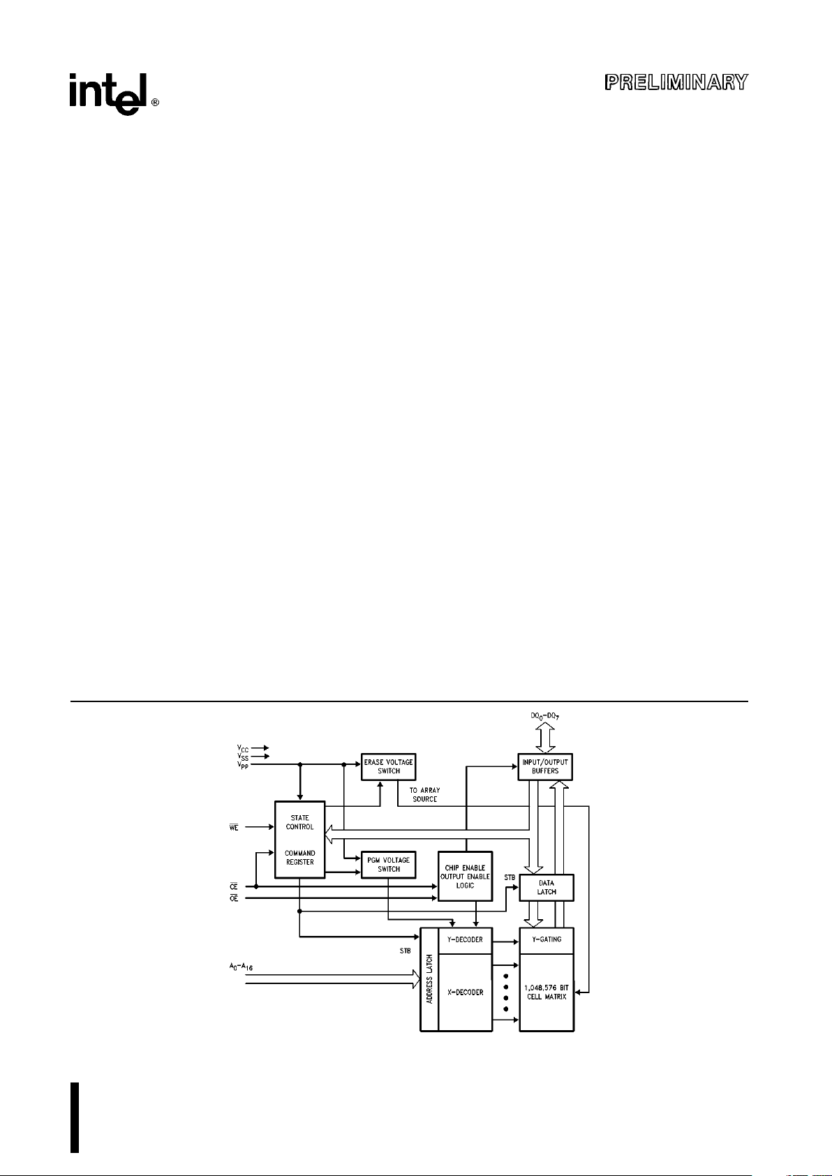
271111–1
Figure 1. M28F010 Block Diagram

M28F010
271111–2
271111–16
271111–3
Figure 2. M28F010 Pin Configurations
Table 1. Pin Description
Symbol Type Name and Function
A0–A
16
INPUT ADDRESS INPUTS for memory addresses. Addresses are internally
latched during a write cycle.
DQ0–DQ
7
INPUT/OUTPUT DATA INPUT/OUTPUT: Inputs data during memory write cycles;
outputs data during memory read cycles. The data pins are active high
and float to tri-state OFF when the chip is deselected or the outputs
are disabled. Data is internally latched during a write cycle.
CE INPUT CHIP ENABLE: Activates the device’s control logic, input buffers,
decoders and sense amplifiers. CE
is active low; CE high deselects the
memory device and reduces power consumption to standby levels.
OE INPUT OUTPUT ENABLE: Gates the devices output through the data buffers
during a read cycle. OE
is active low.
WE INPUT WRITE ENABLE: Controls writes to the control register and the array.
Write enable is active low. Addresses are latched on the falling edge
and data is latched on the rising edge of the WE
pulse.
Note: With V
PP
s
V
CC
a
2V, memory contents cannot be altered.
V
PP
ERASE/PROGRAM POWER SUPPLY for writing the command
register, erasing the entire array, or programming bytes in the array.
V
CC
DEVICE POWER SUPPLY (5Vg10%)
V
SS
GROUND
NC NO INTERNAL CONNECTION to device. Pin may be driven or left
floating.
2
M28F010
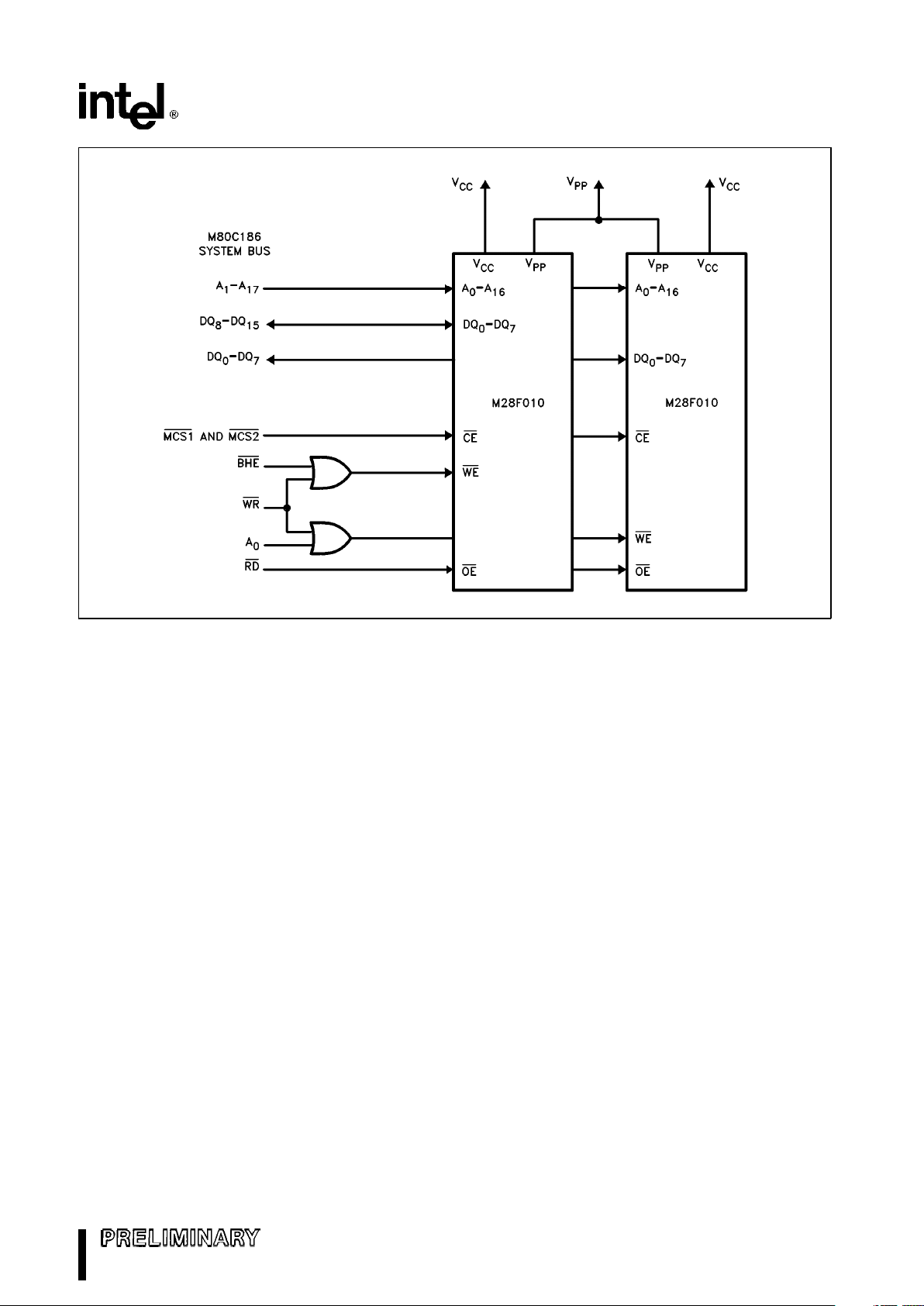
271111–4
Figure 3. M28F010 in a M80C186 System
PRINCIPLES OF OPERATION
Flash-memory augments EPROM functionality with
in-circuit electrical erasure and reprogramming. The
M28F010 introduces a command register to manage
this new functionality. The command register allows
for: 100% TTL-level control inputs; fixed power supplies during erasure and programming; and maximum EPROM compatibility.
In the absence of high voltage on the V
PP
pin, the
M28F010 is a read-only memory. Manipulation of the
external memory-control pins yields the standard
EPROM read, standby, output disable, and intelligent Identifier operations.
The same EPROM read, standby, and output disable
operations are available when high voltage is applied to the V
PP
pin. In addition, high voltage on V
PP
enables erasure and programming of the device. All
functions associated with altering memory contentsÐintelligent Identifier, erase, erase verify, program, and program verifyÐare accessed via the
command register.
Commands are written to the register using standard
microprocessor write timings. Register contents
serve as input to an internal state-machine which
controls the erase and programming circuitry. Write
cycles also internally latch addresses and data
needed for programming or erase operations. With
the appropriate command written to the register,
standard microprocessor read timings output array
data, access the intelligent Identifier codes, or output data for erase and program verification.
The command register is only alterable when V
PP
is
at high voltage. Depending upon the application, the
system designer may choose to make the V
PP
power supply switchableÐavailable only when memory
updates are desired. When high voltage is removed,
the contents of the register default to the read command, making the M28F010 a read-only memory.
Memory contents cannot be altered.
3
M28F010
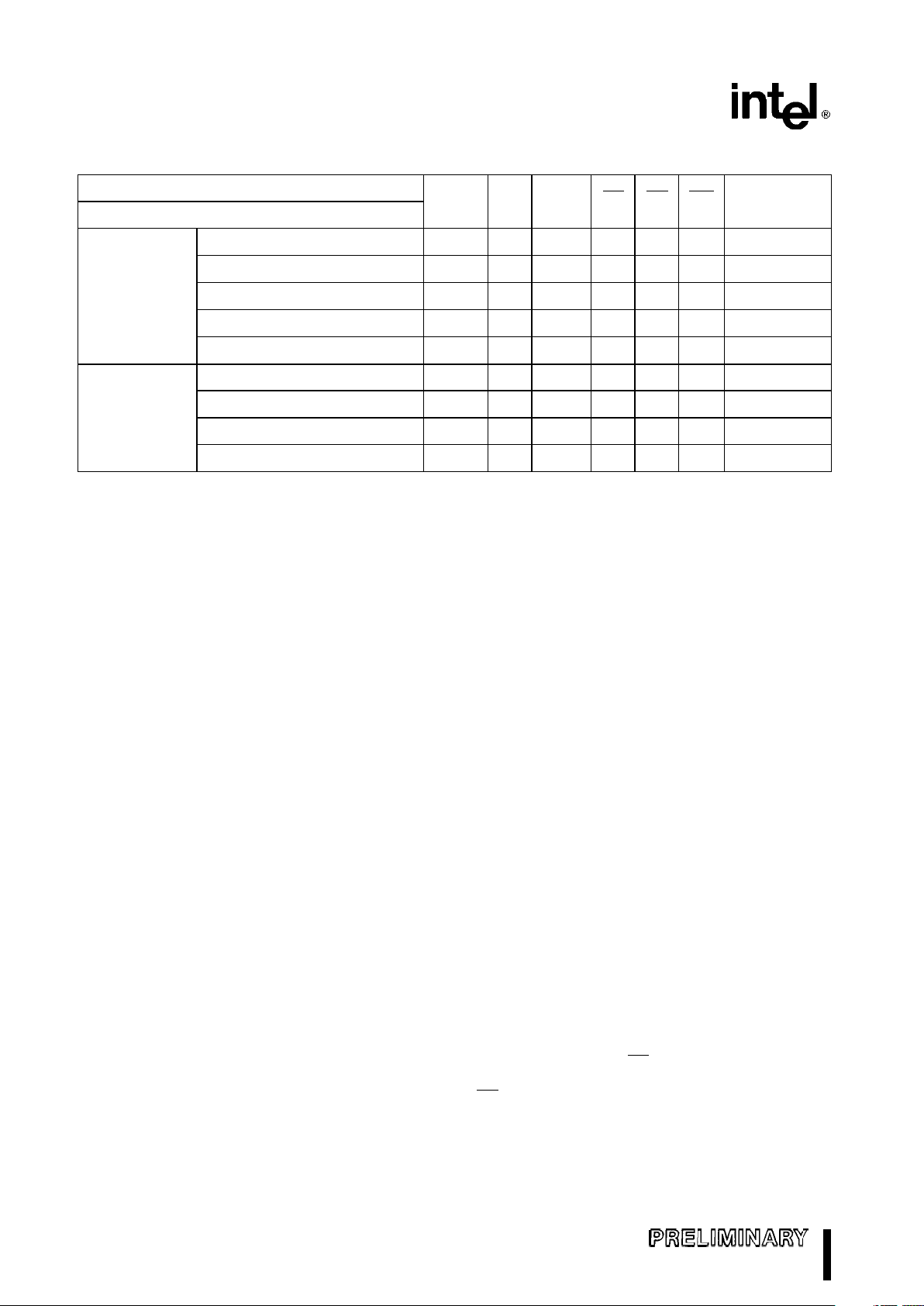
Table 2. M28F010 Bus Operations
Pins
V
PP
(1)
A
0
A
9
CE OE WE DQ0–DQ
7
Operation
Read V
PPL
A
0
A
9
V
IL
V
IL
V
IH
Data Out
Output Disable V
PPL
XXVILV
IH
V
IH
Tri-State
READ-ONLY
Standby V
PPL
XXVIHX X Tri-State
intelligent Identifier (Mfr)
(2)
V
PPL
V
IL
V
ID
(7)
V
IL
V
IL
V
IH
Datae89H
intelligent Identifier (Device)
(2)
V
PPL
V
IHVID
(7)
V
IL
V
IL
V
IH
DataeB4H
Read V
PPH
A
0
A
9
V
IL
V
IL
V
IH
Data Out
(3)
READ/WRITE
Output Disable V
PPH
XXVILV
IH
V
IH
Tri-State
Standby
(4)
V
PPH
XXVIHX X Tri-State
Write V
PPH
A
0
A
9
V
IL
V
IH
V
IL
Data In
(5)
NOTES:
1. V
PPL
may be ground, a no-connect with a resistor tied to ground, or as defined in the Characteristics Section. V
PPH
is the
programming voltage specified for the device. Refer to DC Characteristics. When V
PP
e
V
PPL
memory contents can be
read but not written or erased.
2. Manufacturer and device codes may also be accessed via a command register write sequence. Refer to Table 3. All other
addresses low.
3. Read operations with V
PP
e
V
PPH
may access array data or the intelligent Identifier codes.
4. With V
PP
at high voltage, the standby current equals I
CC
a
I
PP
(standby).
5. Refer to Table 3 for valid Data-In during a write operation.
6. X can be V
IL
or VIH.
7. V
ID
is the intelligent Identifier high voltage. Refer to DC Characteristics.
Or, the system designer may choose to ‘‘hardwire’’
V
PP
, making the high voltage supply constantly
available. In this instance, all operations are performed in conjunction with the command register.
The M28F010 is designed to accommodate either
design practice, and to encourage optimization of
the processor-memory interface.
Integrated Stop Timer
Sucessive command write cycles define the durations of program and erase operations; specifically,
the program or erase time durations are normally
terminated by associated program or erase verify
commands. An integrated stop timer provides simplified timing control over these operations; thus eliminating the need for maximum program/erase timing
specifications. Programming and erase pulse durations are minimums only. When the stop timer terminates a program or erase operation, the device
enters an inactive state and remains inactive until
receiving the appropriate verify or reset command.
Write Protection
The command register is only active when VPPis at
high voltage. Depending upon the application, the
system designer may choose to make the V
PP
pow-
er supply switchableÐavailable only when memory
updates are desired. When V
PP
e
V
PPL
, the contents of the register default to the read command,
making the 28F010 a read-only memory. In this
mode, the memory contents cannot be altered.
Or, the system designer may choose to ‘‘hardwire’’
V
PP
, making the high voltage supply constantly
available. In this case, all Command Register functions are inhibited whenever V
CC
is below the write
lockout voltage V
LKO
. (See Power Up/Down Protection) The 28F010 is designed to accommodate either design practice, and to encourage optimization
of the processor-memory interface.
BUS OPERATIONS
Read
The M28F010 has two control functions, both of
which must be logically active, to obtain data at the
outputs. Chip-Enable (CE
) is the power control and
should be used for device selection. Output-Enable
(OE
) is the output control and should be used
to gate data from the output pins, independent of
device selection. Figure 6 illustrates read timing
waveforms.
4

M28F010
When VPPis high (V
PPH
), the read operation can be
used to access array data, to output the intelligent
Identifier codes, and to access data for program/
erase verification. When V
PP
is low (V
PPL
), the read
operation can only access the array data.
Output Disable
With Output-Enable at a logic-high level (V
IH
), output
from the device is disabled. Output pins are placed
in a high-impedance state.
Standby
With Chip-Enable at a logic-high level, the standby
operation disables most of the M28F010’s circuitry
and substantially reduces device power consumption. The outputs are placed in a high-impedance
state, independent of the Output-Enable signal.
If the M28F010 is deselected during erasure, programming, or program/erase verification, the
device draws active current until the operation is
terminated.
intelligent Identifier Operation
The intelligent Identifier operation outputs the manufacturer code (89H) and device code (B4H). Programming equipment automatically matches the device with its proper erase and programming algorithms.
With Chip-Enable and Output-Enable at a logic low
level, raising A9 to high voltage V
ID
activates the
operation. Data read from locations 0000H and
0001H represent the manufacturer’s code and the
device code, respectively.
The manufacturer- and device-codes can also be
read via the command register, for instances where
the M28F010 is erased and reprogrammed in the
target system. Following a write of 90H to the command register, a read from address location 0000H
outputs the manufacturer code (89H). A read from
address 0001H outputs the device code (B4H).
Write
Device erasure and programming are accomplished
via the command register, when high voltage is applied to the V
PP
pin. The contents of the register
serve as input to the internal state-machine. The
state-machine outputs dictate the function of the
device.
The command register itself does not occupy an addressable memory location. The register is a latch
used to store the command, along with address and
data information needed to execute the command.
The command register is written by bringing WriteEnable to a logic-low level (V
IL
), while Chip-Enable is
low. Addresses are latched on the falling edge of
Write-Enable, while data is latched on the rising
edge of the Write-Enable pulse. Standard microprocessor write timings are used.
The three high-order register bits (R7, R6, R5) encode the control functions. All other register bits, R4
to R0, must be zero. The only exception is the reset
command, when FFH is written to the register. Register bits R7 –R0 correspond to data inputs D7 – D0.
Refer to AC Write Characteristics and the Erase/
Programming Waveforms for specific timing
parameters.
5
M28F010
COMMAND DEFINITIONS
When low voltage is applied to the VPPpin, the contents of the command register default to 00H, enabling read-only operations.
Placing high voltage on the V
PP
pin enables read/
write operations. Device operations are selected by
writing specific data patterns into the command register. Table 3 defines these M28F010 register
commands.
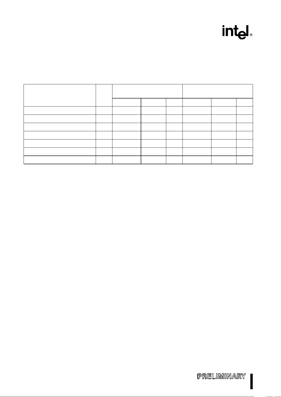
Table 3. Command Definitions
Bus
First Bus Cycle Second Bus Cycle
Command Cycles
Req’d Operation
(1)
Address
(2)
Data
(3)
Operation
(1)
Address
(2)
Data
(3)
Read Memory 1 Write X 00H
Read intelligent Identifier Codes
(4)
2 Write X 90H Read IA ID
Set-up Erase/Erase
(5)
2 Write X 20H Write X 20H
Erase Verify
(5)
2 Write EA A0H Read X EVD
Set-up Program/Program
(6)
2 Write X 40H Write PA PD
Program Verify
(6)
2 Write X C0H Read X PVD
Reset
(7)
2 Write X FFH Write X FFH
NOTES:
1. Bus operations are defined in Table 2.
2. IA
e
Identifier address: 00H for manufacturer code, 01H for device code.
EA
e
Address of memory location to be read during erase verify.
PA
e
Address of memory location to be programmed.
Addresses are latched on the falling edge of the Write-Enable pulse.
3. ID
e
Data read from location IA during device identification (Mfre89H, DeviceeB4H).
EVD
e
Data read from location EA during erase verify.
PD
e
Data to be programmed at location PA. Data is latched on the rising edge of Write-Enable.
PVD
e
Data read from location PA during program verify. PA is latched on the Program command.
4. Following the Read inteligent ID command, two read operations access manufacturer and device codes.
5. Figure 5 illustrates the Quick-Erase Algorithm.
6. Figure 4 illustrates the Quick-Pulse Programming Algorithm.
7. The second bus cycle must be followed by the desired command register write.
6

M28F010
Read Command
While VPPis high, for erasure and programming,
memory contents can be accessed via the read
command. The read operation is initiated by writing
00H into the command register. Microprocessor
read cycles retrieve array data. The device remains
enabled for reads until the command register contents are altered.
The default contents of the register upon V
PP
power-up is 00H. This default value ensures that no spurious alteration of memory contents occurs during
the V
PP
power transition. Where the VPPsupply is
hard-wired to the M28F010, the device powers-up
and remains enabled for reads until the commandregister contents are changed. Refer to the AC
Read Characteristics and Waveforms for specific
timing parameters.
Intelligent Identifier Command
Flash-memories are intended for use in applications
where the local CPU alters memory contents. As
such, manufacturer- and device-codes must be accessible while the device resides in the target system. PROM programmers typically access signature
codes by raising A9 to a high voltage. However, multiplexing high voltage onto address lines is not a desired system-design practice.
The M28F010 contains an intelligent Identifier operation to supplement traditional PROM-programming
methodology. The operation is initiated by writing
90H into the command register. Following the command write, a read cycle from address 0000H retrieves the manufacturer code of 89H. A read cycle
from address 0001H returns the device code of
B4H. To terminate the operation, it is necessary to
write another valid command into the register.
Set-up Erase/Erase Commands
Set-up Erase is a command-only operation that
stages the device for electrical erasure of all bytes in
the array. The set-up erase operation is performed
by writing 20H to the command register.
To commence chip-erasure, the erase command
(20H) must again be written to the register. The
erase operation begins with the rising edge of the
Write-Enable pulse and terminates with the rising
edge of the next Write-Enable pulse (i.e., Erase-Verify Command).
This two-step sequence of set-up followed by execution ensures that memory contents are not accidentally erased. Also, chip-erasure can only occur when
high voltage is applied to the V
PP
pin. In the absence
of this high voltage, memory contents are protected
against erasure. Refer to AC Erase Characteristics
and Waveforms for specific timing parameters.
Erase-Verify Command
The erase command erases all bytes of the array in
parallel. After each erase operation, all bytes must
be verified. The erase verify operation is initiated by
writing A0H into the command register. The address
for the byte to be verified must be supplied as it is
latched on the falling edge of the Write-Enable
pulse. The register write terminates the erase operation with the rising edge of its Write-Enable pulse.
The M28F010 applies an internally-generated margin voltage to the addressed byte. Reading FFH
from the addressed byte indicates that all bits in the
byte are erased.
The erase-verify command must be written to the
command register prior to each byte verification to
latch its address. The process continues for each
byte in the array until a byte does not return FFH
data, or the last address is accessed.
In the case where the data read is not FFH, another
erase operation is performed. (Refer to Set-up
Erase/Erase). Verification then resumes from the
address of the last-verified byte. Once all bytes in
the array have been verified, the erase step is complete. The device can be programmed. At this point,
the verify operation is terminated by writing a valid
command (e.g. Program Set-up) to the command
register. Figure 5, the Quick-Erase algorithm, illustrates how commands and bus operations are combined to perform electrical erasure of the M28F010.
Refer to AC Erase Characteristics and Waveforms
for specific timing parameters.
Set-up Program/Program Commands
Set-up program is a command-only operation that
stages the device for byte programming. Writing 40H
into the command register performs the set-up
operation.
Once the program set-up operation is performed,
the next Write-Enable pulse causes a transition to
an active programming operation. Addresses are internally latched on the falling edge of the Write-Enable pulse. Data is internally latched on the rising
edge of the Write-Enable pulse. The rising edge of
Write-Enable also begins the programming operation. The programming operation terminates with the
next rising edge of Write-Enable, used to write the
program-verify command. Refer to AC Program-
7
 Loading...