Intel Corporation MQ80C286, MA80C286 Datasheet
February 1990 Order Number: 271103-001
M80C286
HIGH PERFORMANCE CHMOS MICROPROCESSOR
WITH MEMORY MANAGEMENT AND PROTECTION
Military
Y
High Speed CHMOS III Technology
Y
Pin for Pin, Clock for Clock, and
Functionally Compatible with the HMOS
M80286
(See M80286 Data Sheet, OrderÝ271028-003)
Y
Stop Clock Capability
Ð Uses Less Power (see I
CCS
Specification)
Y
10 MHz Clock Rate
Y
68 Lead Pin Grid Array Package
Y
68 Lead Ceramic Quad Flatpack
Package
(See Packaging Spec., OrderÝ231369)
Y
Military Temperature Range:
b
55§Ctoa125§C(TC)
INTRODUCTION
The M80C286 is an advanced 16 bit CHMOS III microprocessor designed for multi-user and multi-tasking
applications that require low power and high performance. The M80C286 is fully compatible with its predecessor the HMOS M80286 and object-code compatible with the M8086 and M80386 family of products. In
addition, the M80C286 has a power down mode which uses less power, making it ideal for mobile applications.
The M80C286 has built-in memory protection that maintains a four level protection mechanism for task isolation, a hardware task switching facility and memory mangement capabilities that map 2
30
bytes (one gigabyte)
of virtual address space per task (per user) into 2
24
bytes (16 megabytes) of physical memory.
The M80C286 is upward compatible with M8086 and M8088 software. Using M8086 real address mode, the
M80C286 is object code compatible with existing M8086, M8088 software. In protected virtual address mode,
the M80C286 is source code compatible with M8086, M8088 software which may require upgrading to use
virtual addresses supported by the M80C286’s integrated memory management and protection mechanism.
Both modes operate at full M80C286 performance and execute a superset of the M8086 and M8088 instructions.
The M80C286 provides special operations to support the efficient implementation and execution of operating
systems. For example, one instruction can end execution of one task, save its state, switch to a new task, load
its state, and start execution of the new task. The M80C286 also supports virtual memory systems by providing
a segment-not-present exception and restartable instructions.
271103–1
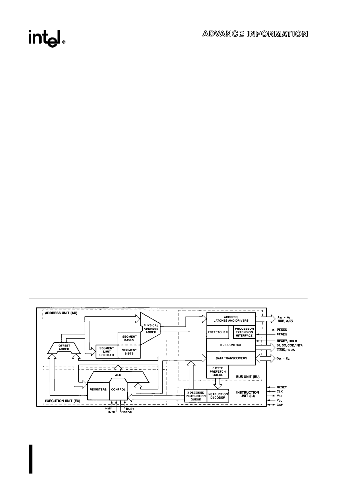
Figure 1. M80C286 Internal Block Diagram
M80C286
FUNCTIONAL DESCRIPTION
Introduction
The M80C286 is an advanced, high-performance microprocessor with specially optimized capabilities for
multiple user and multi-tasking systems. Depending
on the application, a 10 MHz M80C286’s performance is up to eight times faster than the standard 5
MHz M8086’s, while providing complete upward
software compatibility with Intel’s M8086, 88, and
186 family of CPU’s.
The M80C286 operates in two modes: M8086 real
address mode and protected virtual address mode.
Both modes execute a superset of the M8086 and
88 instruction set.
In M8086 real address mode programs use real addresses with up to one megabyte of address space.
Programs use virtual addresses in protected virtual
address mode, also called protected mode. In protected mode, the M80C286 CPU automatically maps
1 gigabyte of virtual addresses per task into a 16
megabyte real address space. This mode also provides memory protection to isolate the operating
system and ensure privacy of each tasks’ programs
and data. Both modes provide the same base instruction set, registers, and addressing modes.
The following Functional Description describes first,
the base M80C286 architecture common to both
modes, second, M8086 real address mode, and
third, protected mode.
M80C286 BASE ARCHITECTURE
The M8086, 88, 186, and 286 CPU family all contain
the same basic set of registers, instructions, and
addressing modes. The M80C286 processor is upward compatible with the M8086, M8088, and 80186
CPU’s and fully compatible with the HMOS M80286.
Register Set
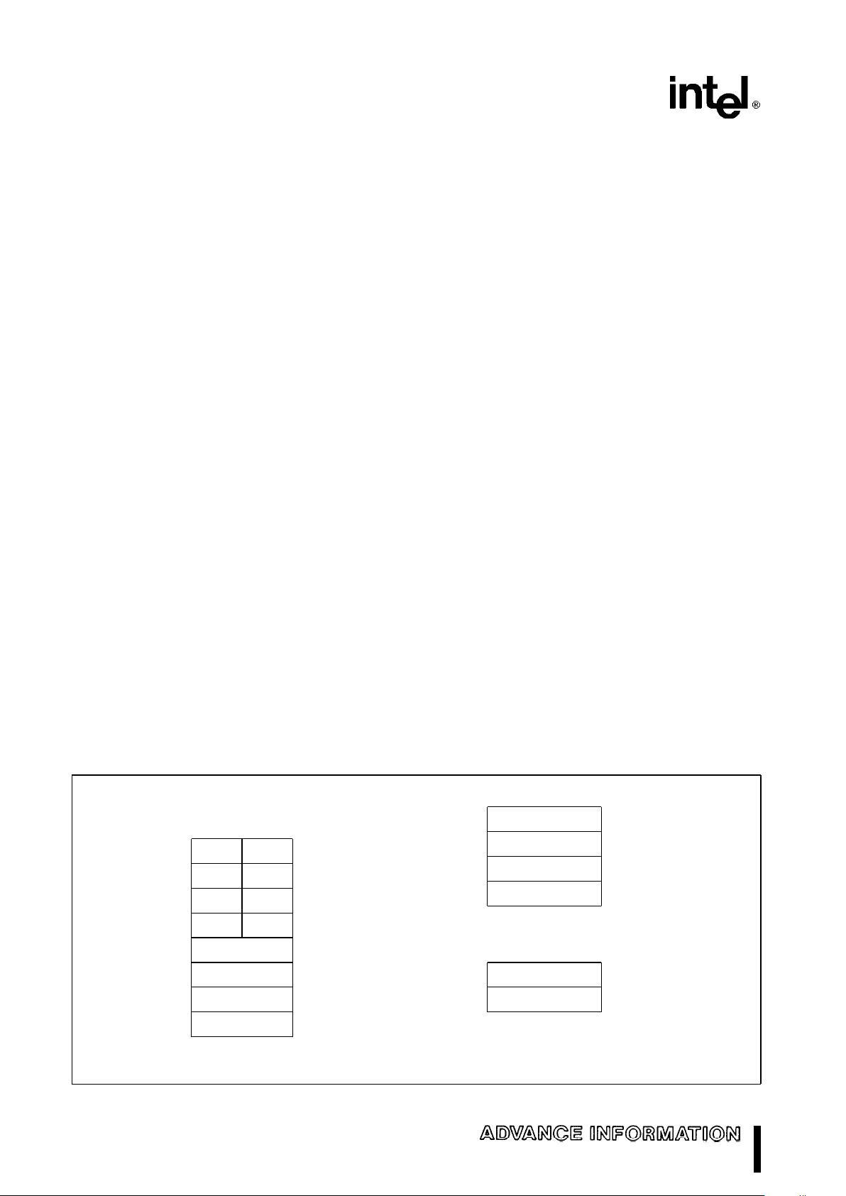
The M80C286 base architecture has fifteen registers
as shown in Figure 2. These registers are grouped
into the following four categories:
General Registers: Eight 16-bit general purpose
registers used to contain arithmetic and logical operands. Four of these (AX, BX, CX, and DX) can be
used either in their entirety as 16-bit words or split
into pairs of separate 8-bit registers.
Segment Registers: Four 16-bit special purpose
registers select, at any given time, the segments of
memory that are immediately addressable for code,
stack, and data. (For usage, refer to Memory Organization.)
Base and Index Registers: Four of the general purpose registers may also be used to determine offset
addresses of operands in memory. These registers
may contain base addresses or indexes to particular
locations within a segment. The addressing mode
determines the specific registers used for operand
address calculations.
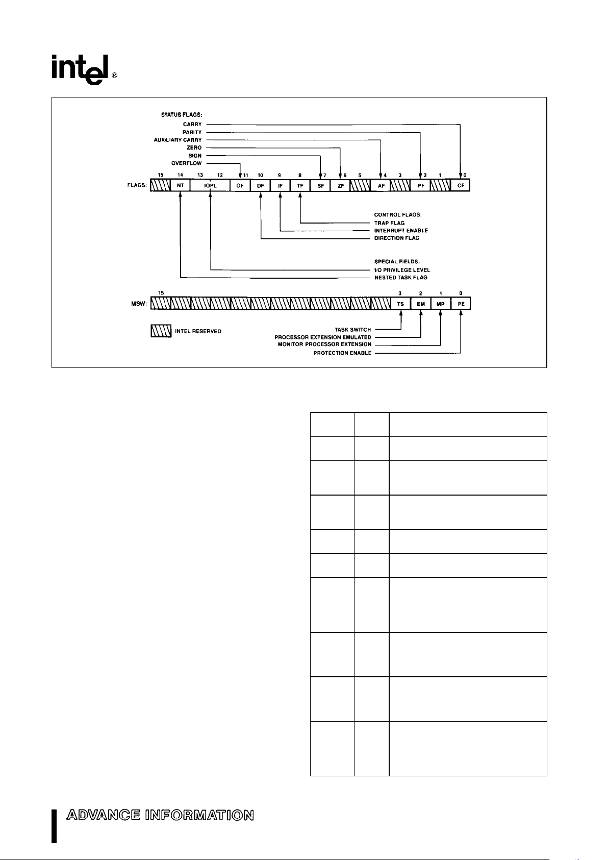
Status and Control Registers: The 3 16-bit special
purpose registers in Figure 3 record or control certain aspects of the M80C286 processor state including the Instruction Pointer, which contains the offset
address of the next sequential instruction to be executed.
16-BIT SPECIAL
REGISTER REGISTER
NAME FUNCTIONS
7070
BYTE
ADDRESSABLE
AX AH AL
MULTIPLY/DIVIDE
REGISTER
(8-BIT
DX DH DL
I/O INSTRUCTIONS
*
SHOWN)
NAMES
CX CH CL
(
LOOP/SHIFT/REPEAT/COUNT
%
BX BH BL
BASE REGISTERS
BP
*
SI
INDEX REGISTERS
DI
*
SP
(
STACK POINTER
15 0
GENERAL
REGISTERS
15 0
CS CODE SEGMENT SELECTOR
DS DATA SEGMENT SELECTOR
SS STACK SEGMENT SELECTOR
ES EXTRA SEGMENT SELECTOR
SEGMENT REGISTERS
15 0
F STATUS WORD
IP INSTRUCTION POINTER
STATUS AND CONTROL
REGISTERS
Figure 2. Register Set
2
M80C286
271103–2
Figure 3. Status and Control Register Bit Functions
Flags Word Description
The Flags word (Flags) records specific characteristics of the result of logical and arithmetic instructions
(bits 0, 2, 4, 6, 7, and 11) and controls the operation
of the M80C286 within a given operating mode (bits
8 and 9). Flags is a 16-bit register. The function of
the flag bits is given in Table 1.
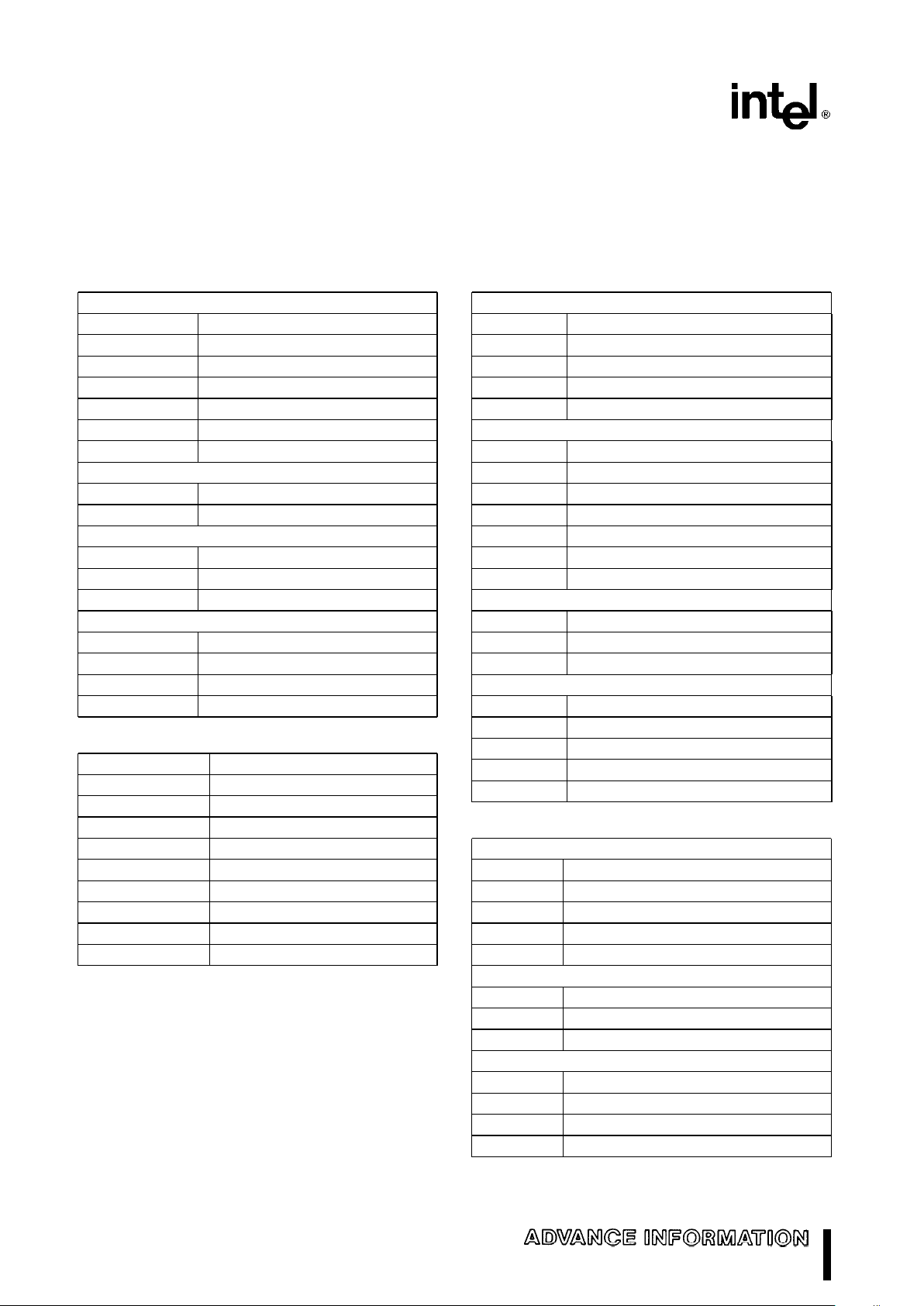
Instruction Set
The instruction set is divided into seven categories:
data transfer, arithmetic, shift/rotate/logical, string
manipulation, control transfer, high level instructions, and processor control. These categories are
summarized in Table 2.
An M80C286 instruction can reference zero, one, or
two operands; where an operand resides in a register, in the instruction itself, or in memory. Zero-operand instructions (e.g. NOP and HLT) are usually one
byte long. One-operand instructions (e.g. INC and
DEC) are usually two bytes long but some are encoded in only one byte. One-operand instructions
may reference a register or memory location. Twooperand instructions permit the following six types of
instruction operations:
ÐRegister to Register
ÐMemory to Register
ÐImmediate to Register
ÐMemory to Memory
ÐRegister to Memory
ÐImmediate to Memory
Table 1. Flags Word Bit Functions
Bit
Name Function
Position
0 CF Carry FlagÐSet on high-order bit
carry or borrow; cleared otherwise
2 PF Parity FlagÐSet if low-order 8 bits
of result contain an even number of
1-bits; cleared otherwise
4 AF Set on carry from or borrow to the
low order four bits of AL; cleared
otherwise
6 ZF Zero FlagÐSet if result is zero;
cleared otherwise
7 SF Sign FlagÐSet equal to high-order
bit of result (0 if positive, 1 if negative)
11 OF Overflow FlagÐSet if result is a too-
large positive number or a too-small
negative number (excluding sign-bit)
to fit in destination operand; cleared
otherwise
8 TF Single Step FlagÐOnce set, a sin-
gle step interrupt occurs after the
next instruction executes. TF is
cleared by the single step interrupt.
9 IF Interrupt-enable FlagÐWhen set,
maskable interrupts will cause the
CPU to transfer control to an interrupt vector specified location.
10 DF Direction FlagÐCauses string
instructions to auto decrement
the appropriate index registers
when set. Clearing DF causes
auto increment.
3
M80C286
Two-operand instructions (e.g. MOV and ADD) are
usually three to six bytes long. Memory to memory
operations are provided by a special class of string
instructions requiring one to three bytes. For detailed instruction formats and encodings refer to the
instruction set summary at the end of this document.
For detailed operation and usage of each instruction, see Appendix B of the 80286/80287 Programmer’s Reference Manual (Order No. 210498).
Table 2. Instruction Set
GENERAL PURPOSE
MOV Move byte or word
PUSH Push word onto stack
POP Pop word off stack
PUSHA Push all registers on stack
POPA Pop all registers from stack
XCHG Exchange byte or word
XLAT Translate byte
INPUT/OUTPUT
IN Input byte or word
OUT Output byte or word
ADDRESS OBJECT
LEA Load effective address
LDS Load pointer using DS
LES Load pointer using ES
FLAG TRANSFER
LAHF Load AH register from flags
SAHF Store AH register in flags
PUSHF Push flags onto stack
POPF Pop flags off stack
Data Transfer Instructions
MOVS Move byte or word string
INS Input bytes or word string
OUTS Output bytes or word string
CMPS Compare byte or word string
SCAS Scan byte or word string
LODS Load byte or word string
STOS Store byte or word string
REP Repeat
REPE/REPZ Repeat while equal/zero
REPNE/REPNZ Repeat while not equal/not zero
String Instructions
ADDITION
ADD Add byte or word
ADC Add byte or word with carry
INC Increment byte or word by 1
AAA ASCII adjust for addition
DAA Decimal adjust for addition
SUBTRACTION
SUB Subtract byte or word
SBB Subtract byte or word with borrow
DEC Decrement byte or word by 1
NEG Negate byte or word
CMP Compare byte or word
AAS ASCII adjust for subtraction
DAS Decimal adjust for subtraction
MULTIPLICATION
MUL Multiple byte or word unsigned
IMUL Integer multiply byte or word
AAM ASCII adjust for multiply
DIVISION
DIV Divide byte or word unsigned
IDIV Integer divide byte or word
AAD ASCII adjust for division
CBW Convert byte to word
CWD Convert word to doubleword
Arithmetic Instructions
LOGICALS
NOT ‘‘Not’’ byte or word
AND ‘‘And’’ byte or word
OR ‘‘Inclusive or’’ byte or word
XOR ‘‘Exclusive or’’ byte or word
TEST ‘‘Test’’ byte or word
SHIFTS
SHL/SAL Shift logical/arithmetic left byte or word
SHR Shift logical right byte or word
SAR Shift arithmetic right byte or word
ROTATES
ROL Rotate left byte or word
ROR Rotate right byte or word
RCL Rotate through carry left byte or word
RCR Rotate through carry right byte or word
Shift/Rotate Logical Instructions
4
M80C286
Table 2. Instruction Set (Continued)
CONDITIONAL TRANSFERS
JA/JNBE Jump if above/not below nor equal
JAE/JNB Jump if above or equal/not below
JB/JNAE Jump if below/not above nor equal
JBE/JNA Jump if below or equal/not above
JC Jump if carry
JE/JZ Jump if equal/zero
JG/JNLE Jump if greater/not less nor equal
JGE/JNL Jump if greater or equal/not less
JL/JNGE Jump if less/not greater nor equal
JLE/JNG Jump if less or equal/not greater
JNC Jump if not carry
JNE/JNZ Jump if not equal/not zero
JNO Jump if not overflow
JNP/JPO Jump if not parity/parity odd
JNS Jump if not sign
JO Jump if overflow
JP/JPE Jump if parity/parity even
JS Jump if sign
UNCONDITIONAL TRANSFERS
CALL Call procedure
RET Return from procedure
JMP Jump
ITERATION CONTROLS
LOOP Loop
LOOPE/LOOPZ Loop if equal/zero
LOOPNE/LOOPNZ Loop if not equal/not zero
JCXZ Jump if register CXe0
INTERRUPTS
INT Interrupt
INTO Interrupt if overflow
IRET Interrupt return
Program Transfer Instructions
FLAG OPERATIONS
STC Set carry flag
CLC Clear carry flag
CMC Complement carry flag
STD Set direction flag
CLD Clear direction flag
STI Set interrupt enable flag
CLI Clear interrupt enable flag
EXTERNAL SYNCHRONIZATION
HLT Halt until interrupt or reset
WAIT Wait for BUSY not active
ESC Escape to extension processor
LOCK Lock bus during next instruction
NO OPERATION
NOP No operation
EXECUTION ENVIRONMENT CONTROL
LMSW Load machine status word
SMSW Store machine status word
Process Control Instructions
ENTER Format stack for procedure entry
LEAVE Restore stack for procedure exit
BOUND Detects values outside
prescribed range
High Level Instructions
Memory Organization
Memory is organized as sets of variable length segments. Each segment is a linear contiguous sequence of up to 64K (2
16
) 8-bit bytes. Memory is
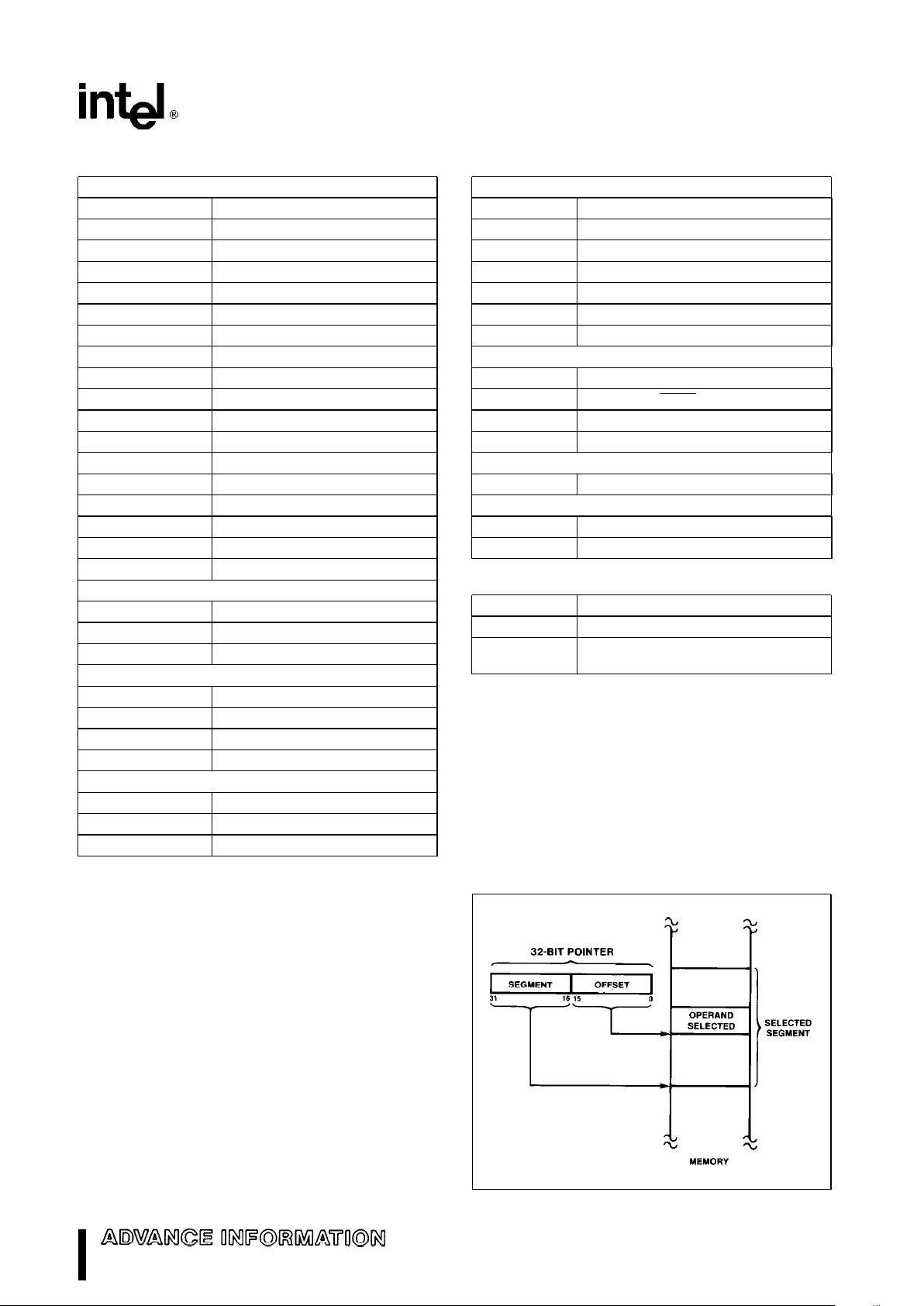
addressed using a two component address (a pointer) that consists of a 16-bit segment selector, and a
16-bit offset, see Figure 4. The segment selector indicates the desired segment in memory. The offset
component indicates the desired byte address within
the segment.
271103–3
Figure 4. Two Component Address
5
M80C286
Table 3. Segment Register Selection Rules
Memory Segment Register Implicit Segment
Reference Needed Used Selection Rule
Instructions Code (CS) Automatic with instruction prefetch
Stack Stack (SS) All stack pushes and pops. Any memory reference which uses BP
as a base register.
Local Data Data (DS) All data references except when relative to stack or
string destination
External (Global) Data Extra (ES) Alternate data segment and destination of string operation
All instructions that address operands in memory
must specify the segment and the offset. For speed
and compact instruction encoding, segment selectors are usually stored in the high speed segment
registers. An instruction need specify only the desired segment register and an offset in order to address a memory operand.
Most instructions need not explicitly specify which
segment register is used. The correct segment register is automatically chosen according to the rules
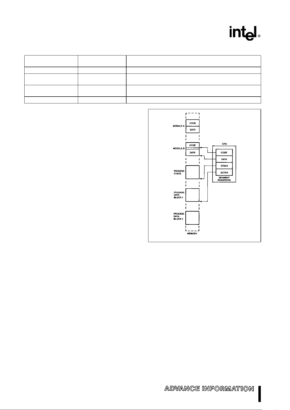
of Table 3. These rules follow the way programs are
written (see Figure 5) as independent modules that
require areas for code and data, a stack, and access
to external data areas.
Special segment override instruction prefixes allow
the implicit segment register selection rules to be
overridden for special cases. The stack, data, and
extra segments may coincide for simple programs.
To access operands not residing in one of the four
immediately available segments, a full 32-bit pointer
or a new segment selector must be loaded.
Addressing Modes
The M80C286 provides a total of eight addressing
modes for instructions to specify operands. Two addressing modes are provided for instructions that
operate on register or immediate operands:
Register Operand Mode: The operand is located in one of the 8 or 16-bit general registers.
Immediate Operand Mode: The operand is included in the instruction.
Six modes are provided to specify the location of an
operand in a memory segment. A memory operand
address consists of two 16-bit components: segment selector and offset. The segment selector is
supplied by a segment register either implicitly chosen by the addressing mode or explicitly chosen by
a segment override prefix. The offset is calculated
by summing any combination of the following three
address elements:
the displacement (an 8 or 16-bit immediate value contained in the instruction)
the base (contents of either the BX or BP base
registers)
271103–4
Figure 5. Segmented Memory Helps
Structure Software
the index (contents of either the SI or DI index
registers)
Any carry out from the 16-bit addition is ignored.
Eight-bit displacements are sign extended to 16-bit
values.
Combinations of these three address elements define the six memory addressing modes, described
below.
Direct Mode: The operand’s offset is contained in
the instruction as an 8 or 16-bit displacement element.
Register Indirect Mode: The operand’s offset is in
one of the registers SI, DI, BX, or BP.
Based Mode: The operand’s offset is the sum of an
8 or 16-bit displacement and the contents of a base
register (BX or BP).
6
M80C286
Indexed Mode: The operand’s offset is the sum of
an 8 or 16-bit displacement and the contents of an
index register (SI or DI).
Based Indexed Mode: The operand’s offset is the
sum of the contents of a base register and an index
register.
Based Indexed Mode with Displacement: The operand’s offset is the sum of a base register’s contents, an index register’s contents, and an 8 or 16-bit
displacement.
Data Types
The M80C286 directly supports the following data
types:
Integer: A signed binary numeric value con-
tained in an 8-bit byte or a 16-bit
word. All operations assume a 2’s
complement representation. Signed
32 and 64-bit integers are supported
using the Numeric Data Processor,
the M80C287.
Ordinal: An unsigned binary numeric value
contained in an 8-bit byte or 16-bit
word.
Pointer: A 32-bit quantity, composed of a
segment selector component and an
offset component. Each component
is a 16-bit word.
String: A contiguous sequence of bytes or
words. A string may contain from 1
byte to 64K bytes.
ASCII: A byte representation of alphanu-
meric and control characters using
the ASCII standard of character representation.
BCD: A byte (unpacked) representation of
the decimal digits 0 –9.
Packed BCD: A byte (packed) representation of
two decimal digits 0 – 9 storing one
digit in each nibble of the byte.
Floating Point: A signed 32, 64, or 80-bit real num-
ber representation. (Floating point
operands are supported using the
M80C287 Numeric Processor).
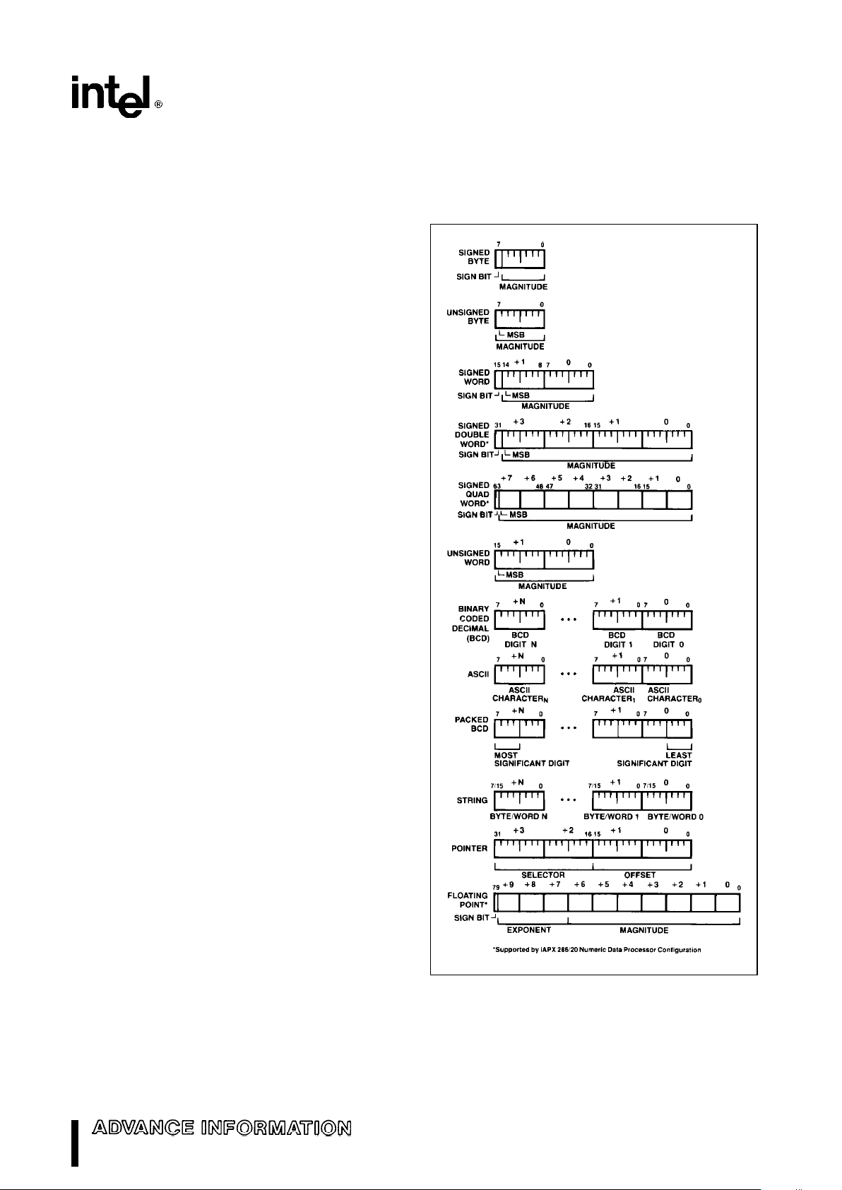
Figure 6 graphically represents the data types supported by the M80C286.
I/O Space
The I/O space consists of 64K 8-bit or 32K 16-bit
ports. I/O instructions address the I/O space with
either an 8-bit port address, specified in the instruction, or a 16-bit port address in the DX register. 8-bit
port addresses are zero extended such that A
15–A8
are LOW. I/O port addresses 00F8(H) through
00FF(H) are reserved.
271103–5
Figure 6. M80C286 Supported Data Types
7

M80C286
Table 4. Interrupt Vector Assignments
Interrupt Related
Does Return Address
Function
Number Instructions
Point to Instruction
Causing Exception?
Divide error exception 0 DIV, IDIV Yes
Single step interrupt 1 All
NMI interrupt 2 INT 2 or NMI pin
Breakpoint interrupt 3 INT 3
INTO detected overflow exception 4 INTO No
BOUND range exceeded exception 5 BOUND Yes
Invalid opcode exception 6 Any undefined opcode Yes
Processor extension not available exception 7 ESC or WAIT Yes
Intel reserved –do not use 8-15
Processor extension error interrupt 16 ESC or WAIT
Intel reserved –do not use 17-31
User defined 32-255
Interrupts
An interrupt transfers execution to a new program
location. The old program address (CS:IP) and machine state (Flags) are saved on the stack to allow
resumption of the interrupted program. Interrupts fall
into three classes: hardware initiated, INT instructions, and instruction exceptions. Hardware initiated
interrupts occur in response to an external input and
are classified as non-maskable or maskable. Programs may cause an interrupt with an INT instruction. Instruction exceptions occur when an unusual
condition, which prevents further instruction processing, is detected while attempting to execute an
instruction. The return address from an exception
will always point at the instruction causing the exception and include any leading instruction prefixes.
A table containing up to 256 pointers defines the
proper interrupt service routine for each interrupt. Interrupts 0– 31, some of which are used for instruction exceptions, are reserved. For each interrupt, an
8-bit vector must be supplied to the M80C286 which
identifies the appropriate table entry. Exceptions
supply the interrupt vector internally. INT instructions
contain or imply the vector and allow access to all
256 interrupts. The Interrupt Vector Assignments are
listed in Table 4. Maskable hardware initiated interrupts supply the 8-bit vector to the CPU during an
interrupt acknowledge bus sequence. Non-maskable hardware interrupts use a predefined internally
supplied vector.
MASKABLE INTERRUPT (INTR)
The M80C286 provides a maskable hardware interrupt request pin, INTR. Software enables this input
by setting the interrupt flag bit (IF) in the flag word.
All 224 user-defined interrupt sources can share this
input, yet they can retain separate interrupt handlers. An 8-bit vector read by the CPU during the
interrupt acknowledge sequence (discussed in System Interface section) identifies the source of the
interrupt.
Further maskable interrupts are disabled while servicing an interrupt by resetting the IF but as part of
the response to an interrupt or exception. The saved
flag word will reflect the enable status of the processor prior to the interrupt. Until the flag word is restored to the flag register, the interrupt flag will be
zero unless specifically set. The interrupt return instruction includes restoring the flag word, thereby
restoring the original status of IF.
NON-MASKABLE INTERRUPT REQUEST (NMI)
A non-maskable interrupt input (NMI) is also provided. NMI has higher priority than INTR. A typical use
of NMI would be to activate a power failure routine.
The activation of this input causes an interrupt with
an internally supplied vector value of 2. No external
interrupt acknowledge sequence is performed.
While executing the NMI servicing procedure, the
M80C286 will service neither further NMI requests,
INTR requests, nor the processor extension segment overrun interrupt until an interrupt return (IRET)
instruction is executed or the CPU is reset. If NMI
occurs while currently servicing an NMI, its presence
will be saved for servicing after executing the first
IRET instruction. IF is cleared at the beginning of an
NMI interrupt to inhibit INTR interrupts.
8
M80C286
SINGLE STEP INTERRUPT
The M80C286 has an internal interrupt that allows
programs to execute one instruction at a time. It is
called the single step interrupt and is controlled by
the single step flag bit (TF) in the flag word. Once
this bit is set, an internal single step interrupt will
occur after the next instruction has been executed.
The interrupt clears the TF bit and uses an internally
supplied vector of 1. The IRET instruction is used to
set the TF bit and transfer control to the next instruction to be single stepped.
Interrupt Priorities
When simultaneous interrupt requests occur, they
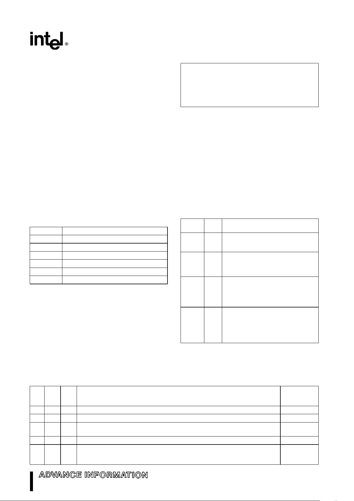
are processed in a fixed order as shown in Table 5.
Interrupt processing involves saving the flags, return
address, and setting CS:IP to point at the first instruction of the interrupt handler. If other interrupts
remain enabled they are processed before the first
instruction of the current interrupt handler is executed. The last interrupt processed is therefore the first
one serviced.
Table 5. Interrupt Processing Order
Order Interrupt
1 Instruction exception
2 Single step
3 NMI
4 Processor extension segment overrun
5 INTR
6 INT instruction
Initialization and Processor Reset
Processor initialization or start up is accomplished
by driving the RESET input pin HIGH. RESET forces
the M80C286 to terminate all execution and local
bus activity. No instruction or bus activity will occur
as long as RESET is active. After RESET becomes
inactive and an internal processing interval elapses,
the M80C286 begins execution in real address
mode with the instruction at physical location
FFFFF0(H). RESET also sets some registers to predefined values as shown in Table 6.
Table6. M80C286 InitialRegisterState after RESET
Flag word 0002(H)
Machine Status Word FFF0(H)
Instruction pointer FFF0(H)
Code segment F000(H)
Data segment 0000(H)
Extra segment 0000(H)
Stack segment 0000(H)
HOLD must not be active during the time from the
leading edge of RESET to 34 CLKs after the trailing
edge of RESET.
Machine Status Word Description
The machine status word (MSW) records when a
task switch takes place and controls the operating
mode of the M80C286. It is a 16-bit register of which
the lower four bits are used. One bit places the CPU
into protected mode, while the other three bits, as
shown in Table 7, control the processor extension
interface. After RESET, this register contains
FFF0(H) which places the M80C286 in M8086 real
address mode.
Table 7. MSW Bit Functions
Bit
Name Function
Position
0 PE Protected mode enable places the
M80C286 into protected mode and
cannot be cleared except by RESET.
1 MP Monitor processor extension allows
WAIT instructions to cause a processor
extension not present exception
(number 7).
2 EM Emulate processor extension causes a
processor extension not present
exception (number 7) on ESC
instructions to allow emulating a
processor extension.
3 TS Task switched indicates the next
instruction using a processor extension
will cause exception 7, allowing software
to test whether the current processor
extension context belongs to the current
task.
The LMSW and SMSW instructions can load and
store the MSW in real address mode. The recommended use of TS, EM, and MP is shown in Table 8.
Table 8. Recommended MSW Encodings For Processor Extension Control
Instructions
TS MP EM Recommended Use Causing
Exception 7
0 0 0 Initial encoding after RESET. M80C286 operation is identical to M8086, 88. None
0 0 1 No processor extension is available. Software will emulate its function. ESC
1 0 1 No processor extension is available. Software will emulate its function. The current ESC
processor extension context may belong to another task.
0 1 0 A processor extension exists. None
1 1 0 A processor extension exists. The current processor extension context may belong to ESC or
another task. The Exception 7 on WAIT allows software to test for an error pending WAIT
from a previous processor extension operation.
9
M80C286
Halt
The HLT instruction stops program execution and
prevents the CPU from using the local bus until restarted. Either NMI, INTR with IF
e
1, or RESET will
force the M80C286 out of halt. If interrupted, the
saved CS:IP will point to the next instruction after
the HLT.
M8086 REAL ADDRESS MODE
The M80C286 executes a fully upward-compatible
superset of the M8086 instruction set in real address
mode. In real address mode the M80C286 is object
code compatible with M8086 and M8088 software.
The real address mode architecture (registers and
addressing modes) is exactly as described in the
M80C286 Base Architecture section of this Functional Description.
Memory Size
Physical memory is a contiguous array of up to
1,048,576 bytes (one megabyte) addressed by pins
A
0
through A19and BHE.A20through A23should be
ignored.
Memory Addressing
In real address mode physical memory is a contiguous array of up to 1,048,576 bytes (one megabyte)
addressed by pins A
0
through A19and BHE. Ad-
dress bits A
20–A23
may not always be zero in real
mode. A
20–A23
should not be used by the system
while the M80C286 is operating in Real Mode.
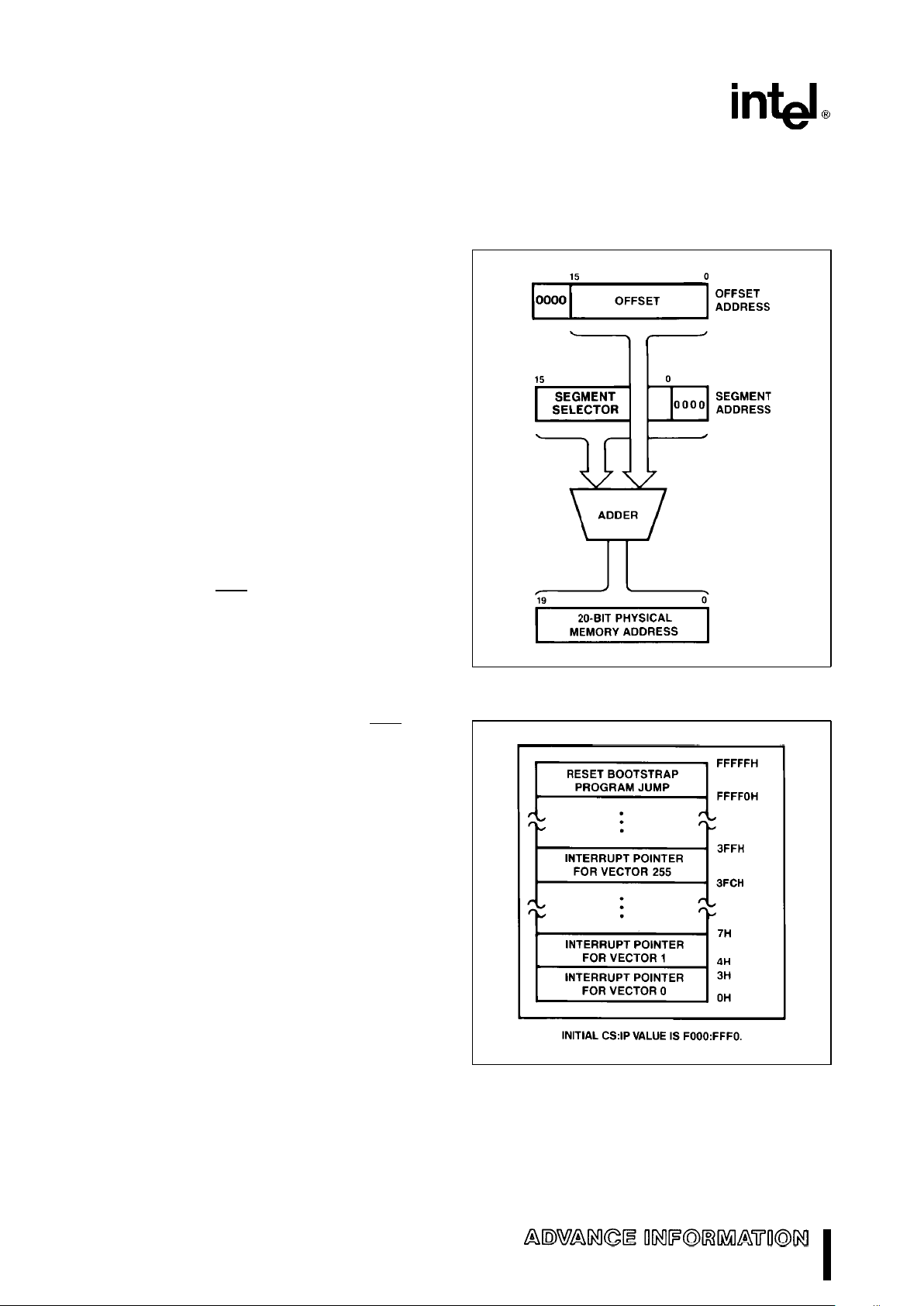
The selector portion of a pointer is interpreted as the
upper 16 bits of a 20-bit segment address. The lower
four bits of the 20-bit segment address are always
zero. Segment addresses, therefore, begin on multiples of 16 bytes. See Figure 7 for a graphic representation of address information.
All segments in real address mode are 64K bytes in
size and may be read, written, or executed. An exception or interrupt can occur if data operands or
instructions attempt to wrap around the end of a
segment (e.g. a word with its low order byte at offset
FFFF(H) and its high order byte at offset 0000(H). If,
in real address mode, the information contained in a
segment does not use the full 64K bytes, the unused
end of the segment may be overlayed by another
segment to reduce physical memory requirements.
Reserved Memory Locations
The M80C286 reserves two fixed areas of memory
in real address mode (see Figure 8); system initiali-
zation area and interrupt table area. Locations from
addresses FFFF0(H) through FFFFF(H) are reserved for system initialization. Initial execution begins at location FFFF0(H). Locations 00000(H)
through 003FF(H) are reserved for interrupt vectors.
271103–6
Figure 7. M8086 Real Address Mode
Address Calculation
271103–7
Figure 8. M8086 Real Address Mode Initially
Reserved Memory Locations
10

M80C286
Table 9. Real Address Mode Addressing Interrupts
Function
Interrupt Related Return Address
Number Instructions Before Instruction?
Interrupt table limit too small exception 8 INT vector is not within table limit Yes
Processor extension segment overrun 9 ESC with memory operand extend- No
interrupt ing beyond offset FFFF(H)
Segment overrun exception 13 Word memory reference with offset Yes
e
FFFF(H) or an attempt to exe-
cute past the end of a segment
Interrupts
Table 9 shows the interrupt vectors reserved for exceptions and interrupts which indicate an addressing
error. The exceptions leave the CPU in the state existing before attempting to execute the failing instruction (except for PUSH, POP, PUSHA, or POPA).
Refer to the next section on protected mode initialization for a discussion on exception 8.
Protected Mode Initialization
To prepare the M80C286 for protected mode, the
LIDT instruction is used to load the 24-bit interrupt
table base and 16-bit limit for the protected mode
interrupt table. This instruction can also set a base
and limit for the interrupt vector table in real address
mode. After reset, the interrupt table base is initialized to 000000(H) and its size set to 03FF(H). These
values are compatible with M8086, 88 software.
LIDT should only be executed in preparation for protected mode.
Shutdown
Shutdown occurs when a severe error is detected
that prevents further instruction processing by the
CPU. Shutdown and halt are externally signalled via
a halt bus operation. They can be distinguished by
A1HIGH for halt and A1LOW for shutdown. In real
address mode, shutdown can occur under two conditions:
#
Exceptions 8 or 13 happen and the IDT limit does
not include the interrupt vector.
#
A CALL INT or PUSH instruction attempts to wrap
around the stack segment when SP is not even.
An NMI input can bring the CPU out of shutdown if
the IDT limit is at least 000F(H) and SP is greater
than 0005(H), otherwise shutdown can only be exited via the RESET input.
PROTECTED VIRTUAL ADDRESS
MODE
The M80C286 executes a fully upward-compatible
superset of the M8086 instruction set in protected
virtual address mode (protected mode). Protected
mode also provides memory management and protection mechanisms and associated instructions.
The M80C286 enters protected virtual address
mode from real address mode by setting the PE
(Protection Enable) bit of the machine status word
with the Load Machine Status Word (LMSW) instruction. Protected mode offers extended physical and
virtual memory address space, memory protection
mechanisms, and new operations to support operating systems and virtual memory.
All registers, instructions, and addressing modes described in the M80C286 Base Architecture section
of this Functional Description remain the same. Programs for the M8086, 88, 186, and real address
mode M80C286 can be run in protected mode; however, embedded constants for segment selectors
are different.
Memory Size
The protected mode M80C286 provides a 1 gigabyte
virtual address space per task mapped into a 16
megabyte physical address space defined by the address pin A
23–A0
and BHE. The virtual address
space may be larger than the physical address
space since any use of an address that does not
map to a physical memory location will cause a restartable exception.
Memory Addressing
As in real address mode, protected mode uses 32bit pointers, consisting of 16-bit selector and offset
components. The selector, however, specifies an index into a memory resident table rather than the upper 16-bits of a real memory address. The 24-bit
base address of the desired segment is obtained
11
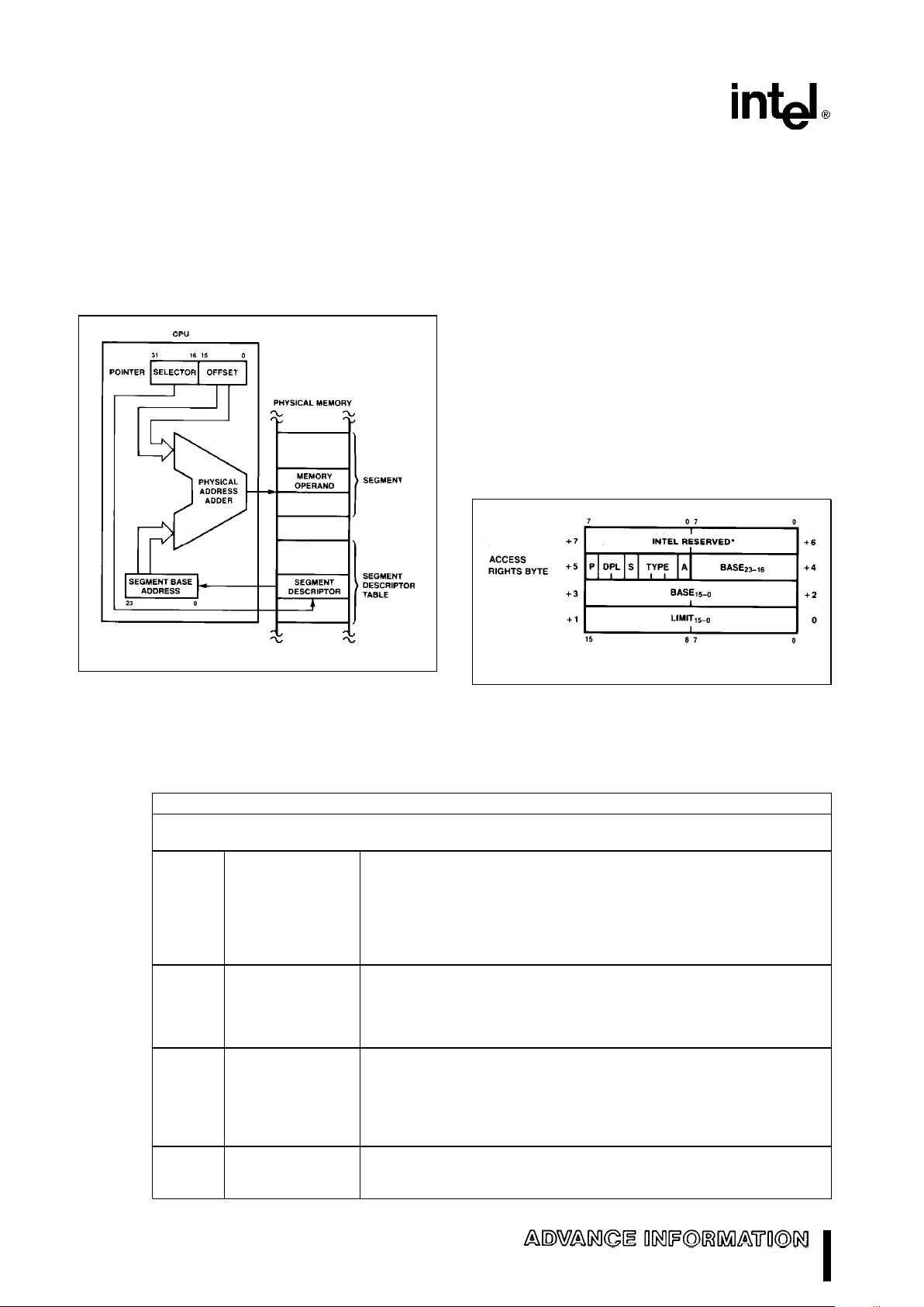
M80C286
from the tables in memory. The 16-bit offset is added to the segment base address to form the physical
address as shown in Figure 10. The tables are automatically referenced by the CPU whenever a segment register is loaded with a selector. All M80C286
instructions which load a segment register will reference the memory based tables without additional
software. The memory based tables contain 8 byte
values called descriptors.
271103–8
Figure 9. Protected Mode Memory Addressing
DESCRIPTORS
Descriptors define the use of memory. Special types
of descriptors also define new functions for transfer
of control and task switching. The M80C286 has
segment descriptors for code, stack and data segments, and system control descriptors for special
system data segments and control transfer operations, see Figure 10. Descriptor accesses are performed as locked bus operations to assure descriptor integrity in multi-processor systems.
CODE AND DATA SEGMENT DESCRIPTORS
(S
e
1)
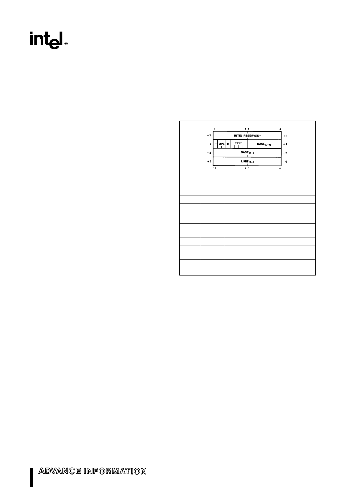
Besides segment base addresses, code and data
descriptors contain other segment attributes including segment size (1 to 64K bytes), access rights
(read only, read/write, execute only, and execute/
read), and presence in memory (for virtual memory
systems) (See Figure 11). Any segment usage violating a segment attribute indicated by the segment
descriptor will prevent the memory cycle and cause
an exception or interrupt.
271103–9
*Must be set to 0 for compatibility with 80386.
Figure 10. Code or Data Segment Descriptor
Access Rights Byte Definition
Bit
Name Function
Position
7 Present (P) Pe1 Segment is mapped into physical memory.
P
e
0 No mapping to physical memory exits, base and limit are
not used.
6–5 Descriptor Privilege Segment privilege attribute used in privilege tests.
Level (DPL)
4 Segment Descrip- Se1 Code or Data (includes stacks) segment descriptor
tor (S) S
e
0 System Segment Descriptor or Gate Descriptor
3 Executable (E) Ee0 Data segment descriptor type is: If
2 Expansion Direc- EDe0 Expand up segment, offsets must beslimit. Data
tion (ED) ED
e
1 Expand down segment, offsets must bellimit. Segment
1 Writeable (W) W
e
0 Data segment may not be written into. (Se1,
Type
W
e
1 Data segment may be written into. *E
e
0)
Field
3 Executable (E) E
e
1 Code Segment Descriptor type is: If
Definition
2 Conforming (C) C
e
1 Code segment may only be executed Code
when CPL
t
DPL and CPL Segment
remains unchanged.
1 Readable (R) R
e
0 Code segment may not be read (Se1,
R
e
1 Code segment may be read. *E
e
1)
0 Accessed (A) Ae0 Segment has not been accessed.
A
e
1 Segment selector has been loaded into segment register
or used by selector test instructions.
Figure 11. Code and Data Segment Descriptor Formats
12
M80C286
Code and data (including stack data) are stored in
two types of segments: code segments and data
segments. Both types are identified and defined by
segment descriptors (S
e
1). Code segments are
identified by the executable (E) bit set to 1 in the
descriptor access rights byte. The access rights byte
of both code and data segment descriptor types
have three fields in common: present (P) bit, Descriptor Privilege Level (DPL), and accessed (A) bit.
If P
e
0, any attempted use of this segment will
cause a not-present exception. DPL specifies the
privilege level of the segment descriptor. DPL controls when the descriptor may be used by a task
(refer to privilege discussion below). The A bit shows
whether the segment has been previously accessed
for usage profiling, a necessity for virtual memory
systems. The CPU will always set this bit when accessing the descriptor.
Data segments (S
e
1, Ee0) may be either readonly or read-write as controlled by the W bit of the
access rights byte. Read-only (W
e
0) data segments may not be written into. Data segments may
grow in two directions, as determined by the Expansion Direction (ED) bit: upwards (ED
e
0) for data
segments, and downwards (ED
e
1) for a segment
containing a stack. The limit field for a data segment
descriptor is interpreted differently depending on the
ED bit (see Figure 11).
A code segment (S
e
1, Ee1) may be executeonly or execute/read as determined by the Readable (R) bit. Code segments may never be written
into and execute-only code segments (R
e
0) may
not be read. A code segment may also have an attribute called conforming (C). A conforming code segment may be shared by programs that execute at
different privilege levels. The DPL of a conforming
code segment defines the range of privilege levels
at which the segment may be executed (refer to privilege discussion below). The limit field identifies the
last byte of a code segment.
SYSTEM SEGMENT DESCRIPTORS (S
e
0,
TYPE
e
1–3)
In addition to code and data segment descriptors,
the protected mode M80C286 defines System Segment Descriptors. These descriptors define special
system data segments which contain a table of descriptors (Local Descriptor Table Descriptor) or segments which contain the execution state of a task
(Task State Segment Descriptor).
Figure 12 gives the formats for the special system
data segment descriptors. The descriptors contain a
24-bit base address of the segment and a 16-bit limit. The access byte defines the type of descriptor, its
state and privilege level. The descriptor contents are
valid and the segment is in physical memory if P
e
1.
If P
e
0, the segment is not valid. The DPL field is
only used in Task State Segment descriptors and
indicates the privilege level at which the descriptor
may be used (see Privilege). Since the Local Descriptor Table descriptor may only be used by a special privileged instruction, the DPL field is not used.
Bit 4 of the access byte is 0 to indicate that it is a
system control descriptor. The type field specifies
the descriptor type as indicated in Figure 12.
System Segment Descriptor
271103–10
*Must be set to 0 for compatibility with 80386.
System Segment Descriptor Fields
Name Value Description
TYPE 1 Available Task State Segment (TSS)
2 Local Descriptor Table
3 Busy Task State Segment (TSS)
P 0 Descriptor contents are not valid
1 Descriptor contents are valid
DPL 0 – 3 Descriptor Privilege Level
BASE 24-bit Base Address of special system data
number segment in real memory
LIMIT 16-bit Offset of last byte in segment
number
Figure 12. System Segment Descriptor Format
GATE DESCRIPTORS (S
e
0, TYPEe4–7)
Gates are used to control access to entry points
within the target code segment. The gate descriptors are call gates, task gates, interrupt gates and
trap gates. Gates provide a level of indirection between the source and destination of the control
transfer. This indirection allows the CPU to automatically perform protection checks and control entry
point of the destination. Call gates are used to
change privilege levels (see Privilege), task gates
are used to perform a task switch, and interrupt and
trap gates are used to specify interrupt service routines. The interrupt gate disables interrupts (resets
IF) while the trap gate does not.
Figure 13 shows the format of the gate descriptors.
The descriptor contains a destination pointer that
points to the descriptor of the target segment and
the entry point offset. The destination selector in an
interrupt gate, trap gate, and call gate must refer to a
code segment descriptor. These gate descriptors
contain the entry point to prevent a program from
constructing and using an illegal entry point. Task
gates may only refer to a task state segment. Since
task gates invoke a task switch, the destination offset is not used in the task gate.
13
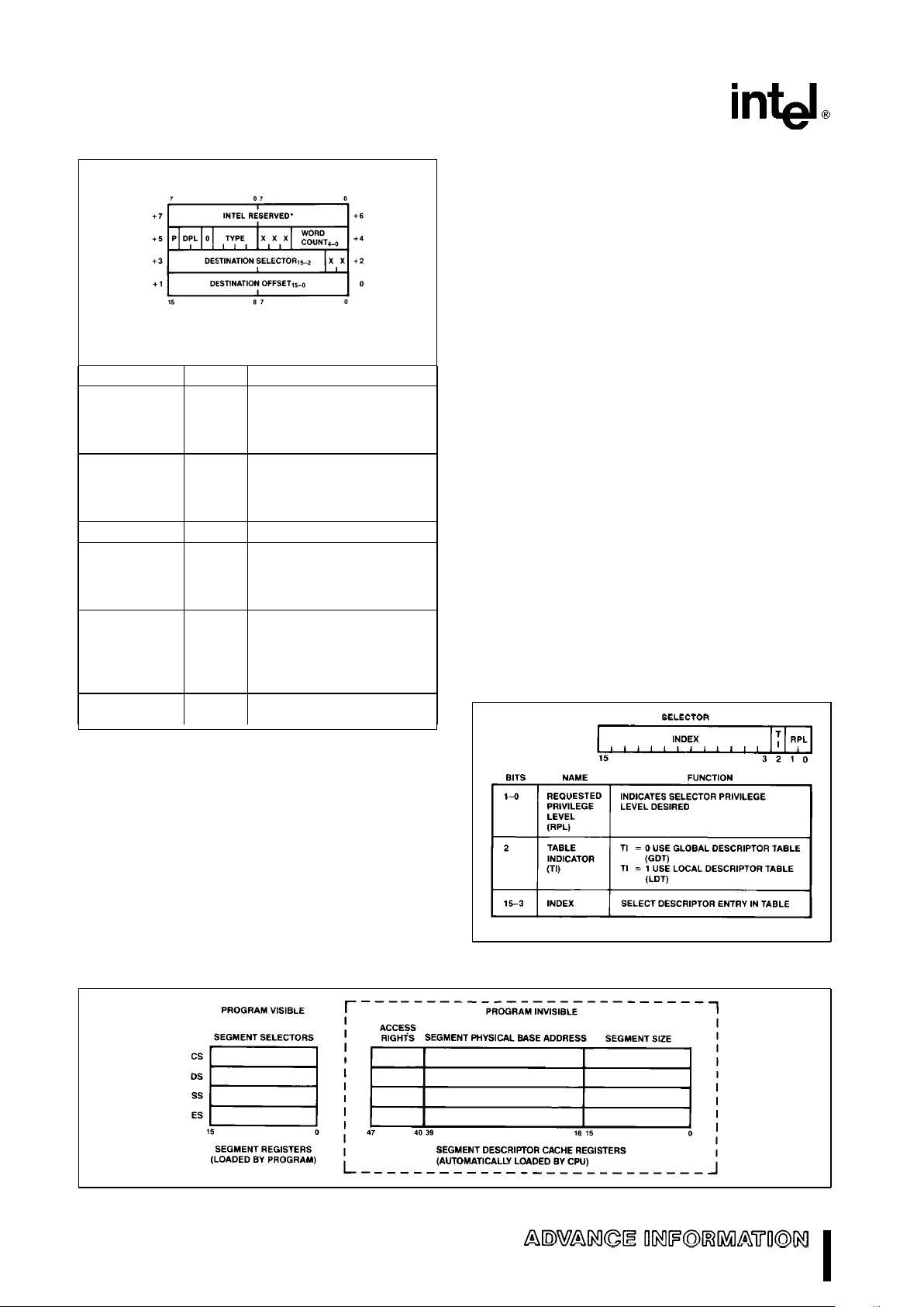
M80C286
Gate Descriptor
271103–11
*Must be set to 0 for compatibility with 80386 (X is don’t care)
Gate Descriptor Fields
Name Value Description
4 –Call Gate
TYPE
5 –Task Gate
6 –Interrupt Gate
7 –Trap Gate
P 0 – Descriptor Contents are not
valid
1 –Descriptor Contents are
valid
DPL 0–3 Descriptor Privilege Level
WORD Number of words to copy
COUNT
0–31
from callers stack to called
procedures stack. Only used
with call gate.
Selector to the target code
DESTINATION 16-bit
segment (Call, Interrupt or
SELECTOR selector
Trap Gate)
Selector to the target task
state segment (Task Gate)
DESTINATION 16-bit Entry point within the target
OFFSET offset code segment
Figure 13. Gate Descriptor Format
Exception 13 is generated when the gate is used if a
destination selector does not refer to the correct descriptor type. The word count field is used in the call
gate descriptor to indicate the number of parameters
(0– 31 words) to be automatically copied from the
caller’s stack to the stack of the called routine when
a control transfer changes privilege levels. The word
count field is not used by any other gate descriptor.
The access byte format is the same for all gate descriptors. P
e
1 indicates that the gate contents are
valid. P
e
0 indicates the contents are not valid and
causes exception 11 if referenced. DPL is the descriptor privilege level and specifies when this descriptor may be used by a task (refer to privilege
discussion below). Bit 4 must equal 0 to indicate a
system control descriptor. The TYPE field specifies
the descriptor type as indicated in Figure 13.
SEGMENT DESCRIPTOR CACHE REGISTERS
A segment descriptor cache register is assigned to
each of the four segment registers (CS, SS, DS, ES).
Segment descriptors are automatically loaded
(cached) into a segment descriptor cache register
(Figure 14) whenever the associated segment register is loaded with a selector. Only segment descriptors may be loaded into segment descriptor cache
registers. Once loaded, all references to that segment of memory use the cached descriptor information instead of reaccessing the descriptor. The descriptor cache registers are not visible to programs.
No instructions exist to store their contents. They
only change when a segment register is loaded.
SELECTOR FIELDS
A protected mode selector has three fields: descriptor entry index, local or global descriptor table indicator (TI), and selector privilege (RPL) as shown in
Figure 15. These fields select one of two memory
based tables of descriptors, select the appropriate
table entry and allow highspeed testing of the selector’s privilege attribute (refer to privilege discussion
below).
271103–12
Figure 15. Selector Fields
271103–13
Figure 14. Descriptor Cache Registers
14
M80C286
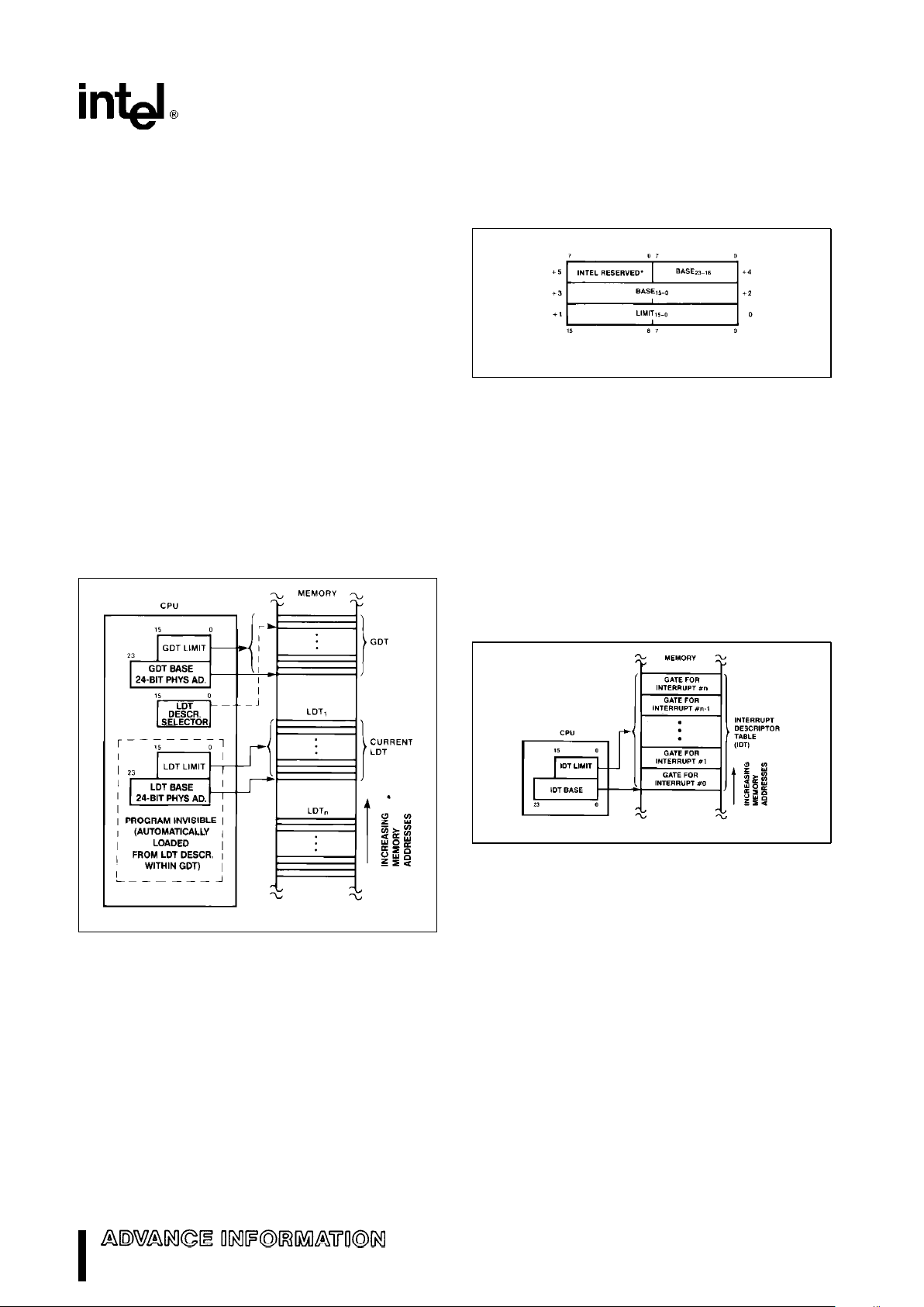
LOCAL AND GLOBAL DESCRIPTOR TABLES
Two tables of descriptors, called descriptor tables,
contain all descriptors accessible by a task at any
given time. A descriptor table is a linear array of up
to 8192 descriptors. The upper 13 bits of the selector value are an index into a descriptor table. Each
table has a 24-bit base register to locate the descriptor table in physical memory and a 16-bit limit register that confine descriptor access to the defined limits of the table as shown in Figure 16. A restartable
exception (13) will occur if an attempt is made to
reference a descriptor outside the table limits.
One table, called the Global Descriptor table (GDT),
contains descriptors available to all tasks. The other
table, called the Local Descriptor Table (LDT), contains descriptors that can be private to a task. Each
task may have its own private LDT. The GDT may
contain all descriptor types except interrupt and trap
descriptors. The LDT may contain only segment,
task gate, and call gate descriptors. A segment cannot be accessed by a task if its segment descriptor
does not exist in either descriptor table at the time of
access.
271103–14
Figure 16. Local and Global
Descriptor Table Definition
The LGDT and LLDT instructions load the base and
limit of the global and local descriptor tables. LGDT
and LLDT are privileged, i.e. they may only be executed by trusted programs operating at level 0. The
LGDT instruction loads a six byte field containing the
16-bit table limit and 24-bit physical base address of
the Global Descriptor Table as shown in Figure 17.
The LDT instruction loads a selector which refers to
a Local Descriptor Table descriptor containing the
base address and limit for an LDT, as shown in Figure 16.
271103–15
*Must be set to 0 for compatibility with 80386.
Figure 17. Global Descriptor Table and
Interrupt Descriptor Table Data Type
INTERRUPT DESCRIPTOR TABLE
The protected mode M80C286 has a third descriptor
table, called the Interrupt Descriptor Table (IDT)
(see Figure 18), used to define up to 256 interrupts.
It may contain only task gates, interrupt gates and
trap gates. The IDT (Interrupt Descriptor Table) has
a 24-bit physical base and 16-bit limit register in the
CPU. The privileged LIDT instruction loads these
registers with a six byte value of identical form to
that of the LGDT instruction (see Figure 17 and Protected Mode Initialization).
271103–16
Figure 18. Interrupt Descriptor Table Definition
References to IDT entries are made via INT instructions, external interrupt vectors, or exceptions. The
IDT must be at least 256 bytes in size to allocate
space for all reserved interrupts.
Privilege
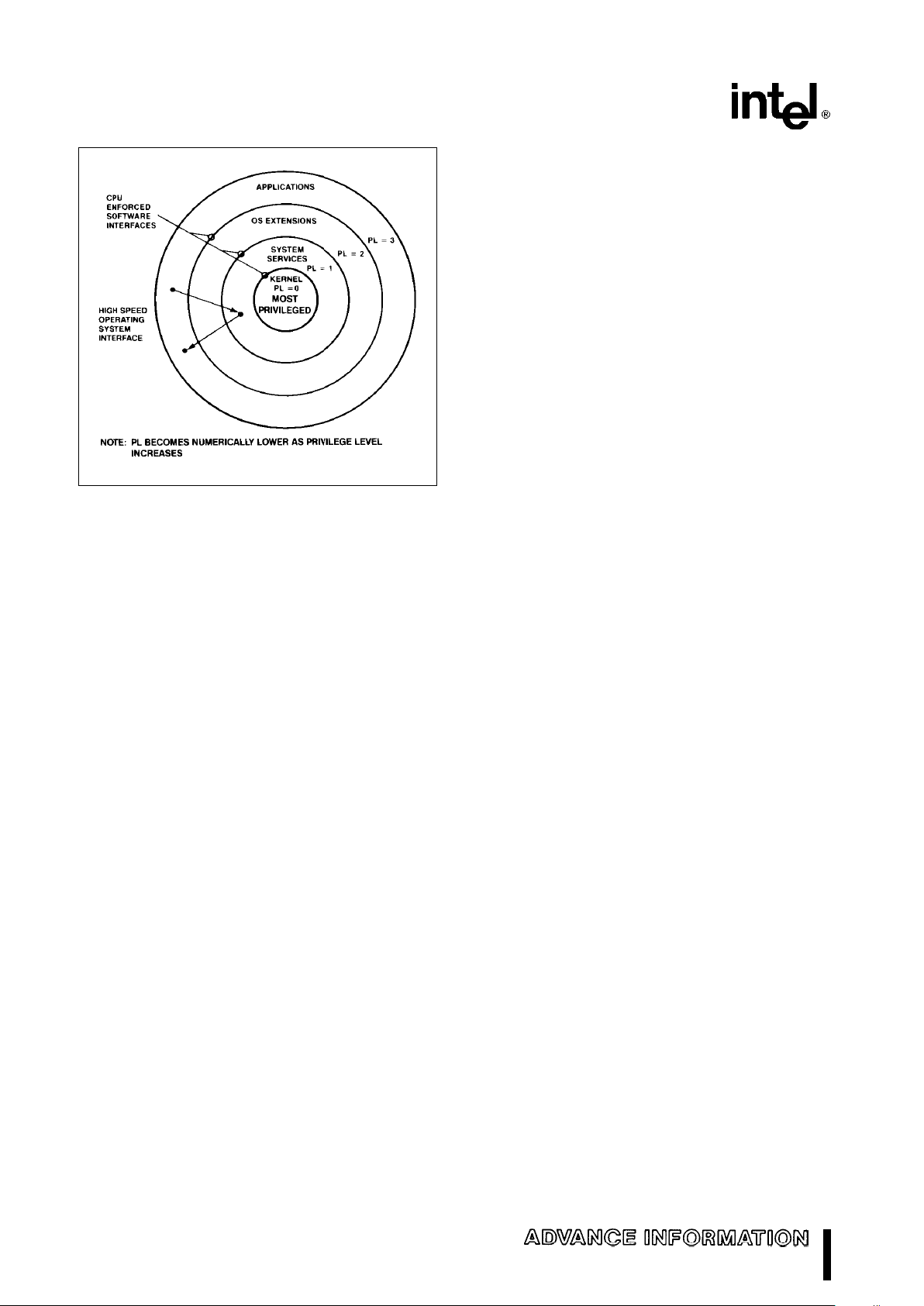
The M80C286 has a four-level hierarchical privilege
system which controls the use of privileged instructions and access to descriptors (and their associated segments) within a task. Four-level privilege, as
shown in Figure 19, is an extension of the user/supervisor mode commonly found in minicomputers.
The privilege levels are numbered 0 through 3.
15
M80C286
271103–17
Figure 19. Privilege Levels
Level 0 is the most privileged level. Privilege levels
provide protection within a task. (Tasks are isolated
by providing private LDT’s for each task.) Operating
system routines, interrupt handlers, and other system software can be included and protected within
the virtual address space of each task using the four
levels of privilege. Each task in the system has a
separate stack for each of its privilege levels.
Tasks, descriptors, and selectors have a privilege
level attribute that determines whether the descriptor may be used. Task privilege effects the use of
instructions and descriptors. Descriptor and selector
privilege only effect access to the descriptor.
TASK PRIVILEGE
A task always executes at one of the four privilege
levels. The task privilege level at any specific instant
is called the Current Privilege Level (CPL) and is defined by the lower two bits of the CS register. CPL
cannot change during execution in a single code
segment. A task’s CPL may only be changed by control transfers through gate descriptors to a new code
segment (See Control Transfer). Tasks begin executing at the CPL value specified by the code segment selector within TSS when the task is initiated
via a task switch operation (See Figure 20). A task
executing at Level 0 can access all data segments
defined in the GDT and the task’s LDT and is considered the most trusted level. A task executing a
Level 3 has the most restricted access to data and is
considered the least trusted level.
DESCRIPTOR PRIVILEGE
Descriptor privilege is specified by the Descriptor
Privilege Level (DPL) field of the descriptor access
byte. DPL specifies the least trusted task privilege
level (CPL) at which a task may access the descriptor. Descriptors with DPL
e
0 are the most protected. Only tasks executing at privilege level 0
(CPL
e
0) may access them. Descriptors with DPL
e
3 are the least protected (i.e. have the least restricted access) since tasks can access them when
CPL
e
0, 1, 2, or 3. This rule applies to all descrip-
tors, except LDT descriptors.
SELECTOR PRIVILEGE
Selector privilege is specified by the Requested Privilege Level (RPL) field in the least significant two bits
of a selector. Selector RPL may establish a less
trusted privilege level than the current privilege level
for the use of a selector. This level is called the
task’s effective privilege level (EPL). RPL can only
reduce the scope of a task’s access to data with this
selector. A task’s effective privilege is the numeric
maximum of RPL and CPL. A selector with RPL
e
0
imposes no additional restriction on its use while a
selector with RPL
e
3 can only refer to segments at
privilege Level 3 regardless of the task’s CPL. RPL
is generally used to verify that pointer parameters
passed to a more trusted procedure are not allowed
to use data at a more privileged level than the caller
(refer to pointer testing instructions).
Descriptor Access and Privilege
Validation
Determining the ability of a task to access a segment involves the type of segment to be accessed,
the instruction used, the type of descriptor used and
CPL, RPL, and DPL. The two basic types of segment
accesses are control transfer (selectors loaded into
CS) and data (selectors loaded into DS, ES or SS).
DATA SEGMENT ACCESS
Instructions that load selectors into DS and ES must
refer to a data segment descriptor or readable code
segment descriptor. The CPL of the task and the
RPL of the selector must be the same as or more
privileged (numerically equal to or lower than) than
the descriptor DPL. In general, a task can only access data segments at the same or less privileged
levels than the CPL or RPL (whichever is numerically
higher) to prevent a program from accessing data it
cannot be trusted to use.
An exception to the rule is a readable conforming
code segment. This type of code segment can be
read from any privilege level.
If the privilege checks fail (e.g. DPL is numerically
less than the maximum of CPL and RPL) or an incorrect type of descriptor is referenced (e.g. gate de-
16
M80C286
scriptor or execute only code segment) exception 13
occurs. If the segment is not present, exception 11
is generated.
Instructions that load selectors into SS must refer to
data segment descriptors for writable data segments. The descriptor privilege (DPL) and RPL must
equal CPL. All other descriptor types or a privilege
level violation will cause exception 13. A not present
fault causes exception 12.
CONTROL TRANSFER
Four types of control transfer can occur when a selector is loaded into CS by a control transfer operation (see Table 10). Each transfer type can only occur if the operation which loaded the selector references the correct descriptor type. Any violation of
these descriptor usage rules (e.g. JMP through a call
gate or RET to a Task State Segment) will cause
exception 13.
The ability to reference a descriptor for control transfer is also subject to rules of privilege. A CALL or
JUMP instruction may only reference a code segment descriptor with DPL equal to the task CPL or a
conforming segment with DPL of equal or greater
privilege than CPL. The RPL of the selector used to
reference the code descriptor must have as much
privilege as CPL.
RET and IRET instructions may only reference code
segment descriptors with descriptor privilege equal
to or less privileged than the task CPL. The selector
loaded into CS is the return address from the stack.
After the return, the selector RPL is the task’s new
CPL. If CPL changes, the old stack pointer is popped
after the return address.
When a JMP or CALL references a Task State Segment descriptor, the descriptor DPL must be the
same or less privileged than the task’s CPL. Refer-
ence to a valid Task State Segment descriptor causes a task switch (see Task Switch Operation). Reference to a Task State Segment descriptor at a more
privileged level than the task’s CPL generates exception 13.
When an instruction or interrupt references a gate
descriptor, the gate DPL must have the same or less
privilege than the task CPL. If DPL is at a more privileged level than CPL, exeception 13 occurs. If the
destination selector contained in the gate references a code segment descriptor, the code segment descriptor DPL must be the same or more privileged than the task CPL. If not, Exception 13 is issued. After the control transfer, the code segment
descriptors DPL is the task’s new CPL. If the destination selector in the gate references a task state
segment, a task switch is automatically performed
(see Task Switch Operation).
The privilege rules on control transfer require:
Ð JMP or CALL direct to a code segment (code
segment descriptor) can only be to a conforming
segment with DPL of equal or greater privilege
than CPL or a non-conforming segment at the
same privilege level.
Ð interrupts within the task or calls that may
change privilege levels, can only transfer control
through a gate at the same or a less privileged
level than CPL to a code segment at the same or
more privileged level than CPL.
Ð return instructions that don’t switch tasks can
only return control to a code segment at the
same or less privileged level.
Ð task switch can be performed by a call, jump or
interrupt which references either a task gate or
task state segment at the same or less privileged
level.
Table 10. Descriptor Types Used for Control Transfer
Control Transfer Types Operation Types
Descriptor Descriptor
Referenced Table
Intersegment within the same privilege level JMP, CALL, RET, IRET* Code Segment GDT/LDT
Intersegment to the same or higher privilege level Interrupt CALL Call Gate GDT/LDT
within task may change CPL.
Interrupt Instruction, Trap or IDT
Exception, External Interrupt
Interrupt Gate
Intersegment to a lower privilege level (changes task CPL) RET, IRET* Code Segment GDT/LDT
CALL, JMP Task State GDT
Segment
Task Switch
CALL, JMP Task Gate GDT/LDT
IRET**
Interrupt Instruction,
Task Gate IDT
Exception, External
Interrupt
*NT (Nested Task bit of flag word)e0
**NT (Nested Task bit of flag word)
e
1
17

M80C286
PRIVILEGE LEVEL CHANGES
Any control transfer that changes CPL within the
task, causes a change of stacks as part of the operation. Initial values of SS:SP for privilege levels 0, 1,
and 2 are kept in the task state segment (refer to
Task Switch Operation). During a JMP or CALL control transfer, the new stack pointer is loaded into the
SS and SP registers and the previous stack pointer
is pushed onto the new stack.
When returning to the original privilege level, its
stack is restored as part of the RET or IRET instruction operation. For subroutine calls that pass parameters on the stack and cross privilege levels, a fixed
number of words, as specified in the gate, are copied from the previous stack to the current stack. The
inter-segment RET instruction with a stack adjustment value will correctly restore the previous stack
pointer upon return.
Protection
The M80C286 includes mechanisms to protect critical instructions that affect the CPU execution state
(e.g. HLT) and code or data segments from improper
usage. These protection mechanisms are grouped
into three forms:
Restricted
usage
of segments (e.g. no write allowed to read-only data segments). The only segments available for use are defined by descriptors in the Local Descriptor Table (LDT) and
Global Descriptor Table (GDT).
Restricted
access
to segments via the rules of
privilege and descriptor usage.
Privileged instructions
or operations that may
only be executed at certain privilege levels as determined by the CPL and I/O Privilege Level
(IOPL). The IOPL is defined by bits 14 and 13 of
the flag word.
These checks are performed for all instructions and
can be split into three categories: segment load
checks (Table 11), operand reference checks (Table
12), and privileged instruction checks (Table 13).
Any violation of the rules shown will result in an exception. A not-present exception related to the stack
segment causes exception 12.
The IRET and POPF instructions do not perform
some of their defined functions if CPL is not of sufficient privilege (numerically small enough). Precisely
these are:
#
The IF bit is not changed if CPLlIOPL.
#
The IOPL field of the flag word is not changed if
CPL
l
0.
No exceptions or other indication are given when
these conditions occur.
Table 11. Segment Register Load Checks
Error Description
Exception
Number
Descriptor table limit exceeded 13
Segment descriptor not-present 11 or 12
Privilege rules violated 13
Invalid descriptor/segment type segment register load:
ÐRead only data segment load to
SS
ÐSpecial Control descriptor load to
DS, ES, SS 13
ÐExecute only segment load to
DS, ES, SS
ÐData segment load to CS
ÐRead/Execute code segment
load to SS
Table 12. Operand Reference Checks
Error Description
Exception
Number
Write into code segment 13
Read from execute-only code
segment 13
Write to read-only data segment 13
Segment limit exceeded
1
12 or 13
NOTE:
Carry out in offset calculations is ignored.
Table 13. Privileged Instruction Checks
Error Description
Exception
Number
CPLi0 when executing the following
instructions:
13
LIDT, LLDT, LGDT, LTR, LMSW,
CTS, HLT
CPLlIOPL when executing the following instructions:
13
INS, IN, OUTS, OUT, STI, CLI,
LOCK
EXCEPTIONS
The M80C286 detects several types of exceptions
and interrupts, in protected mode (see Table 14).
Most are restartable after the exceptional condition
is removed. Interrupt handlers for most exceptions
can read an error code, pushed on the stack after
the return address, that identifies the selector involved (0 if none). The return address normally
points to the failing instruction, including all leading
prefixes. For a processor extension segment overrun exception, the return address will not point at the
ESC instruction that caused the exception; however,
the processor extension registers may contain the
address of the failing instruction.
18
 Loading...