Intel Corporation MQ80C186, MA80C186 Datasheet
November 1993 Order Number: 270500-008
M80C186
CHMOS HIGH INTEGRATION 16-BIT MICROPROCESSOR
Military
Y
Operation Modes Include:
Ð Enhanced Mode Which Has
Ð DRAM Refresh
Ð Power-Save Logic
Ð Direct Interface to New CMOS
Numerics Coprocessor
Ð Compatible Mode
Ð NMOS M80186 Pin-for-Pin
Replacement for Non-Numerics
Applications
Y
Integrated Feature Set
Ð Enhanced M80C86/C88 CPU
Ð Clock Generator
Ð 2 Independent DMA Channels
Ð Programmable Interrupt Controller
Ð 3 Programmable 16-Bit Timers
Ð Dynamic RAM Refresh Control Unit
Ð Programmable Memory and
Peripheral Chip Select Logic
Ð Programmable Wait State Generator
Ð Local Bus Controller
Ð Power Save Logic
Ð System-Level Testing Support (High
Impedance Test Mode)
Y
Available in 10 MHz and 12.5 MHz
Versions
Y
Direct Addressing Capability to
1 Mbyte and 64 Kbyte I/O
Y
Completely Object Code Compatible
with All Existing M8086/M8088
Software and Also Has 10 Additional
Instructions over M8086/M8088
Y
Complete System Development
Support
Ð All M8086 and NMOS M80186
Software Development Tools Can Be
Used for M80C186 System
Development
Ð Assembler, PL/M, Pascal, Fortran,
and System Utilities
Ð In-Circuit-Emulator (ICE
TM
-C186)
Y
Available in 68-Pin Ceramic Pin Grid
Array (PGA) and 68-Lead Ceramic Quad
Flat Pack
(See Packaging Outlines and Dimensions, OrderÝ231369)
Y
Available in Two Product Grades:
Ð MIL-STD-883,
b
55§Ctoa125§C(TC)
Ð Military Temperature Only (MTO),
b
55§Ctoa125§C(TC)
The Intel M80C186 is a CHMOS high integration microprocessor. It has features which are new to the M80186
family which include a DRAM refresh control unit, power-save mode and a direct numerics interface. When
used in ‘‘compatible’’ mode, the M80C186 is 100% pin-for-pin compatible with the NMOS M80186 (except for
M8087 applications). The ‘‘enhanced’’ mode of operation allows the full feature set of the M80C186 to be
used. The M80C186 is upward compatible with M8086 and M8088 software and fully compatible with M80186
and M80188 software.
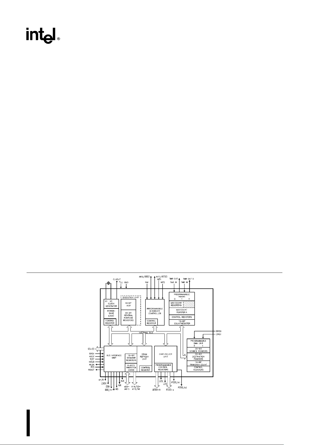
270500–1
Figure 1. M80C186 Block Diagram
M80C186
Pin Grid Array
270500–30
Quad Flat Pack
270500–31
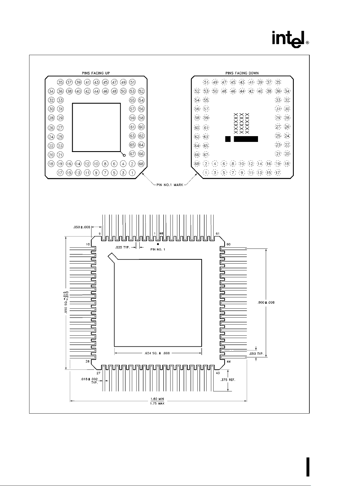
Figure 2. M80C186 Pinout Diagram
For additional packaging information refer to ‘‘Packaging Outlines and Dimensions’’, Order Number 231369
2
M80C186
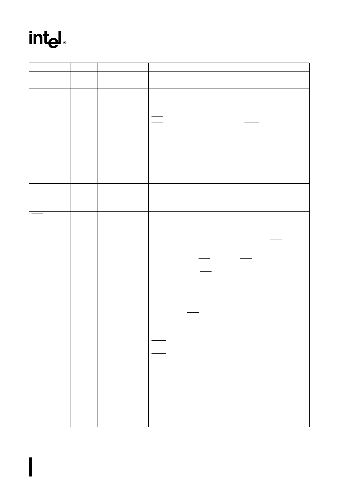
Table 1. M80C186 Pin Description
Symbol PGA QFP Type Name and Function
VCC,V
CC
9, 43 1, 35 I System Power:a5 volt power supply.
VSS,V
SS
26, 60 52, 18 I System Ground.
RESET 57 21 O Reset Output indicates that the M80C186 CPU is being
reset, and can be used as a system reset. It is active HIGH,
synchronized with the processor clock, and lasts an integer
number of clock periods corresponding to the length of the
RES
signal. Reset goes inactive 2 clockout periods after
RES
goes inactive. When tied to the TEST/BUSY pin, Reset
forces the M80C186 into enhanced mode.
X1, X2 59, 58 19, 20 I Crystal Inputs X1 and X2 provide external connections for a
fundamental mode or third overtone parallel resonant crystal
for the internal oscillator. X1 can connect to an external
clock instead of a crystal. In this case, minimize the
capacitance on X2 or drive X2 with complemented X1. The
input or oscillator frequency is internally divided by two to
generate the clock signal (CLKOUT).
CLKOUT 56 22 O Clock Output provides the system with a 50% duty cycle
waveform. All device pin timings are specified relative to
CLKOUT. CLKOUT has sufficient MOS drive capabilities for
the Numeric Processor Extension.
RES 24 54 I System Reset causes the M80C186 to immediately
terminate its present activity, clear the internal logic, and
enter a dormant state. This signal may be asynchronous to
the M80C186 clock. The M80C186 begins fetching
instructions approximately 7 clock cycles after RES is
returned HIGH. For proper initialization, V
CC
must be within
specifications and the clock signal must be stable for more
than 4 clocks with RES
held LOW. RES is internally
synchronized. This input is provided with a Schmitt-trigger to
facilitate power-on RES
generation via an RC network. When
RES
occurs, the M80C186 will drive the status lines to an
inactive level for one clock, and then float them.
TEST/BUSY 47 31 I The TEST pin is sampled during and after reset to determine
whether the M80C186 is to enter Compatible or Enhanced
Mode. Enhanced Mode requires TEST
to be HIGH on the
rising edge of RES
and LOW four clocks later. Any other
combination will place the M80C186 in Compatible Mode. A
weak internal pullup insures a HIGH state when the pin is not
driven.
TEST
ÐIn Compatible Mode this pin is configured to operate
as TEST
. This pin is examined by the WAIT instruction. If the
TEST
input is HIGH when WAIT execution begins, instruction
execution will suspend. TEST
will be resampled every five
clocks until it goes LOW, at which time execution will resume.
If interrupts are enabled while the M80C186 is waiting for
TEST
, interrupts will be serviced.
BUSYÐIn Enhanced Mode, this pin is configured to operate
as BUSY. The BUSY input is used to notify the M80C186 of
Numerics Processor Extension activity. Floating point
instructions executing in the M80C186 sample the BUSY pin
to determine when the Numerics Processor is ready to
accept a new command. BUSY is active HIGH.
3
M80C186
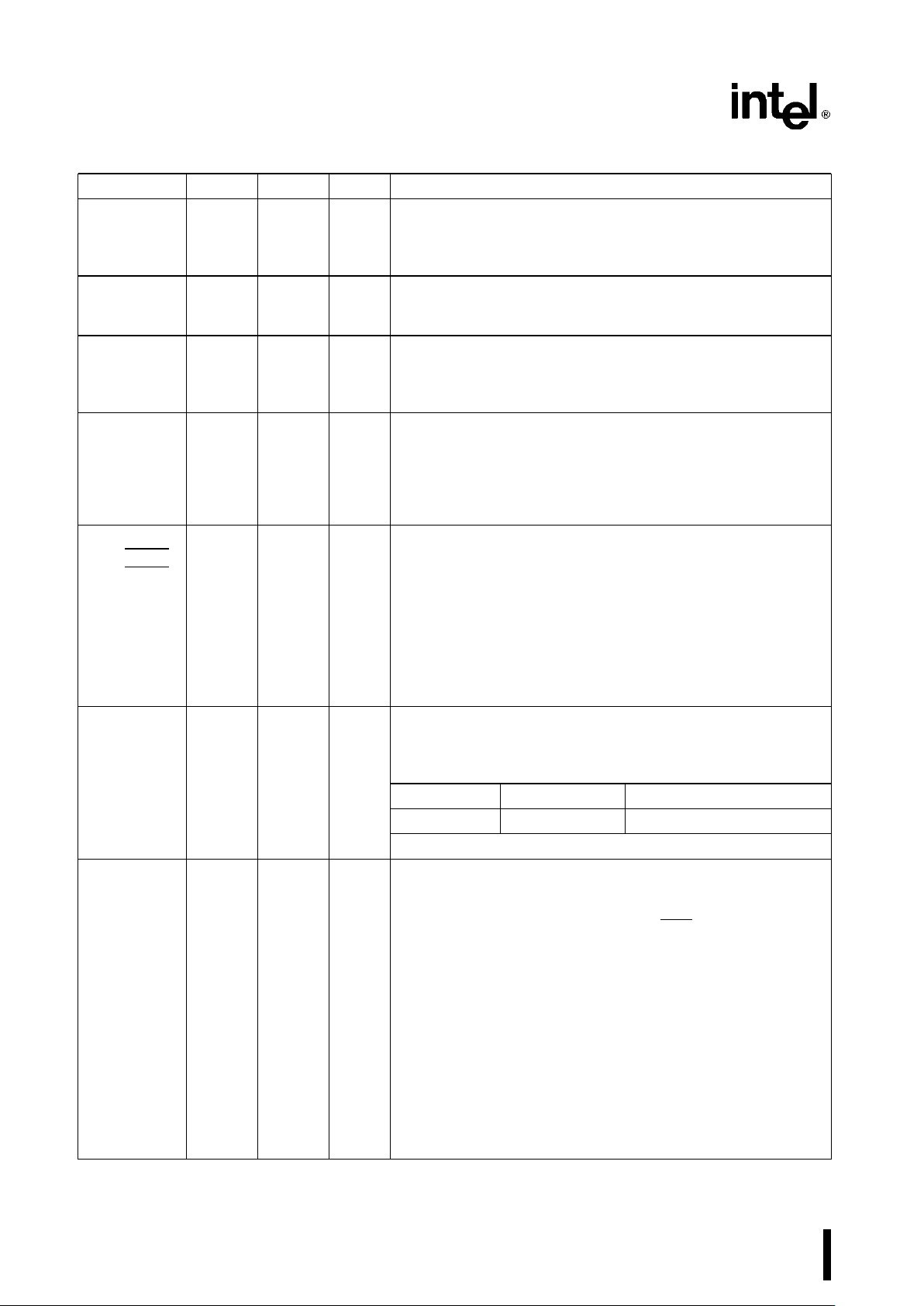
Table 1. M80C186 Pin Description (Continued)
Symbol PGA QFP Type Name and Function
TMR IN 1
TMR IN 0, 20
21
58
57 I
I Timer Inputs are used either as clock or control signals,
depending upon the programmed timer mode. These inputs
are active HIGH (or LOW-to-HIGH transitions are counted) and
internally synchronized.
TMR OUT 0,
TMR OUT 1 23
22 56
55 O
O Timer outputs are used to provide single pulse or continous
waveform generation, depending upon the timer mode
selected.
DRQ1
DRQ0 18
19 59
60 I
I
DMA Request is driven HIGH by an external device when it
desires that a DMA channel (Channel 0 or 1) perform a
transfer. These signals are active HIGH, level-triggered, and
internally synchronized.
NMI 46 32 I Non-Maskable Interrupt is an edge-triggered input which
causes a type 2 interrupt. NMI is not maskable internally. A
transition from a LOW to HIGH initiates the interrupt at the
next instruction boundary. NMI is latched internally. An NMI
duration of one clock or more will guarantee service. This input
is internally synchronized.
INT0, INT1
INT3/INTA1
INT2/INTA0
45, 44
41
42
33, 34
37
36
I/O
I/O
I Maskable Interrupt Requests can be requested by activating
one of these pins. When configured as inputs, these pins are
active HIGH. Interrupt Requests are synchronized internally.
INT2 and INT3 may be configured via software to provide
active-LOW interrupt-acknowledge output signals. All interrupt
inputs may be configured via software to be either edge- or
level-triggered. To ensure recognition, all interrupt requests
must remain active until the interrupt is acknowledged. When
slave mode is selected, the function of these pins changes
(see Interrupt Controller section of this data sheet).
A19/S6,
A16/S3
A17/S4,
A18/S5,
65
68
67
66
13
10
11
12
O
O
O
O
Address Bus Outputs (16 –19) and Bus Cycle Status (3 –6)
reflect the four most significant address bits during T1. These
signals are active HIGH. During T
2,T3,TW
, and T4, status
information is available on these lines as encoded below:
Low High
S6 Processor Cycle DMA Cycle
S3, S4, and S5 are defined as LOW during T2–T4.
AD15 1 9 I/O Address/Data Bus (0– 15) signals constitute the time
multiplexed memory or I/O address (T
1
) and data (T2,T3,TW,
AD14 3 7
and T
4
) bus. The
AD13 5 5
AD12 7 3 bus is active HIGH. A
0
is analogous to BHE for the lower byte
of the data bus, pins D
7
through D0. It is LOW during T1when
AD11 10 68
a byte is to be transferred onto the lower portion of the bus in
AD10 12 66
memory or I/O operations.
AD9 14 64
AD8 16 62
AD7 2 8
AD6 4 6
AD5 6 4
AD4 8 2
AD3 11 67
AD2 13 65
AD1 15 63
AD0 17 61
4
M80C186
Table 1. M80C186 Pin Description (Continued)
Symbol PGA QFP Type Name and Function
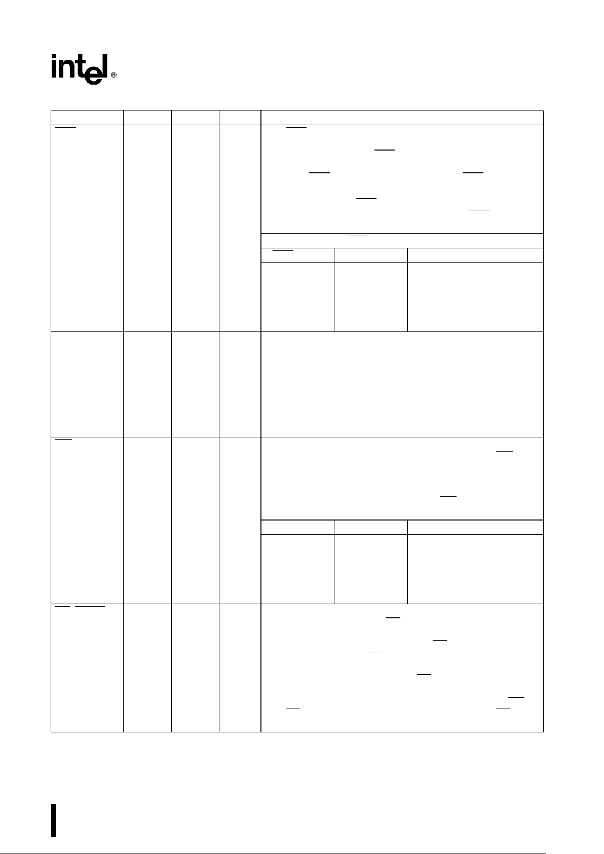
BHE 64 14 O The BHE (Bus High Enable) signal is analogous to A0 in that
it is used to enable data on to the most significant half of the
data bus, pins D15 –D8. BHE
will be LOW during T1when the
upper byte is transferred and will remain LOW through T
3
AND TW. BHE does not need to be latched. BHE will float
during HOLD.
In Enhanced Mode, BHE will also be used to signify DRAM
refresh cycles. A refresh cycle is indicated by BHE
and A0
being HIGH.
BHE and A0 Encodings
BHE Value A0 Value Function
0 0 Word Transfer
0 1 Byte Transfer on upper half
of data bus (D15 –D8)
1 0 Byte Transfer on lower half
of data bus (D
7–D0
)
1 1 Refresh
ALE/QS0 61 17 O Address Latch Enable/Queue Status 0 is provided by the
M80C186 to latch the address. ALE is active HIGH.
Addresses are guaranteed to be valid on the trailing edge of
ALE. The ALE rising edge is generated off the rising edge of
the CLKOUT immediately preceding T1of the associated bus
cycle, effectively one-half clock cycle earlier than in the
standard M8086. The trailing edge is generated off the
CLKOUT rising edge in T
1
as in the M8086. Note that ALE is
never floated.
WR/QS1 63 15 O Write Strobe/Queue Status 1 indicates that the data on the
bus is to be written into a memory or an I/O device. WR
is
active for T
2,T3
, and TWof any write cycle. It is active LOW,
and floats during ‘‘HOLD.’’ It is driven HIGH for one clock
during Reset, and then floated. When the M80C186 is in
queue status mode, the ALE/QS0 and WR
/QS1 pins provide
information about processor/instruction queue interaction.
QS1 QS0 Queue Operation
0 0 No queue operation
0 1 First opcode byte fetched
from the queue
1 1 Subsequent byte fetched
from the queue
1 0 Empty the queue
RD/QSMD 62 16 O Read Strobe indicates that the M80C186 is performing a
memory or I/O read cycle. RD
is active LOW for T2,T3, and
T
W
of any read cycle. It is guaranteed not to go LOW in T
2
until after the Address Bus is floated. RD is active LOW, and
floats during ‘‘HOLD’’. RD is driven HIGH for one clock
during Reset, and then the output driver is floated. A weak
internal pull-up mechanism of the RD
line holds it HIGH when
the line is not driven. During RESET the pin is sampled to
determine whether the M80C186 should provide ALE, WR
and RD, or if the Queue-Status should be provided. RD
should be connected to GND to provide Queue-Status data.
5
M80C186
Table 1. M80C186 Pin Description (Continued)
Symbol PGA QFP Type Name and Function
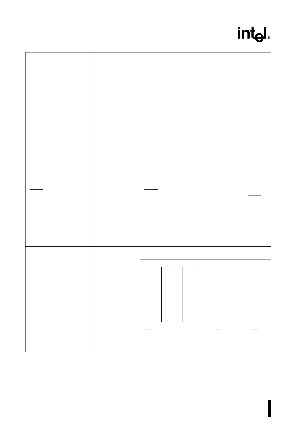
ARDY 55 23 I Asynchronous Ready informs the M80C186 that the
addressed memory space or I/O device will complete
a data transfer. The ARDY input pin will accept an
asynchronous input, and is active HIGH. Only the rising
edge is internally synchronized by the M80C186. This
means that the falling edge of ARDY must be
synchronized to the M80C186 clock. If connected to
V
CC
, no WAIT states are inserted. Asynchronous ready
(ARDY) or synchronous ready (SRDY) must be active
to terminate a bus cycle. If unused, this line should be
tied LOW to yield control to the SRDY pin.
SRDY 49 29 I Synchronous Ready must be synchronized externally
to the M80C186. The use of SRDY provides a relaxed
system-timing specification on the Ready input. This is
accomplished by eliminating the one-half clock cycle
which is required for internally resolving the signal level
when using the ARDY input. This line is active HIGH. If
this line is connected to V
CC
, no WAIT states are
inserted. Asynchronous ready (ARDY) or synchronous
ready (SRDY) must be active before a bus cycle is
terminated. If unused, this line should be tied LOW to
yield control to the ARDY pin.
LOCK 48 30 O LOCK output indicates that other system bus masters
are not to gain control of the system bus while LOCK
is
active LOW. The LOCK
signal is requested by the
LOCK prefix instruction and is activated at the
beginning of the first data cycle associated with the
instruction following the LOCK prefix. It remains active
until the completion of the instruction following the
LOCK prefix. No prefetches will occur while LOCK is
asserted. LOCK
is active LOW, is driven HIGH for one
clock during RESET, and then floated.
S0,S1,S2 52, 53, 54 26, 25, 24 O Bus cycle status S0–S2 are encoded to provide bus-
transaction information:
M80C186 Bus Cycle Status Information
S2 S1 S0 Bus Cycle Initiated
0 0 0 Interrupt Acknowledge
0 0 1 Read I/O
0 1 0 Write I/O
0 1 1 Halt
1 0 0 Instruction Fetch
1 0 1 Read Data from Memory
1 1 0 Write Data to Memory
1 1 1 Passive (no bus cycle)
The status pins float during HOLD/HLDA.
S2
may be used as a logical M/IO indicator, and S1 as
a DT/R
indicator.
The status lines are driven HIGH for one clock during
Reset, and then floated until a bus cycle begins.
6
M80C186
Table 1. M80C186 Pin Description (Continued)
Symbol PGA QFP Type Name and Function
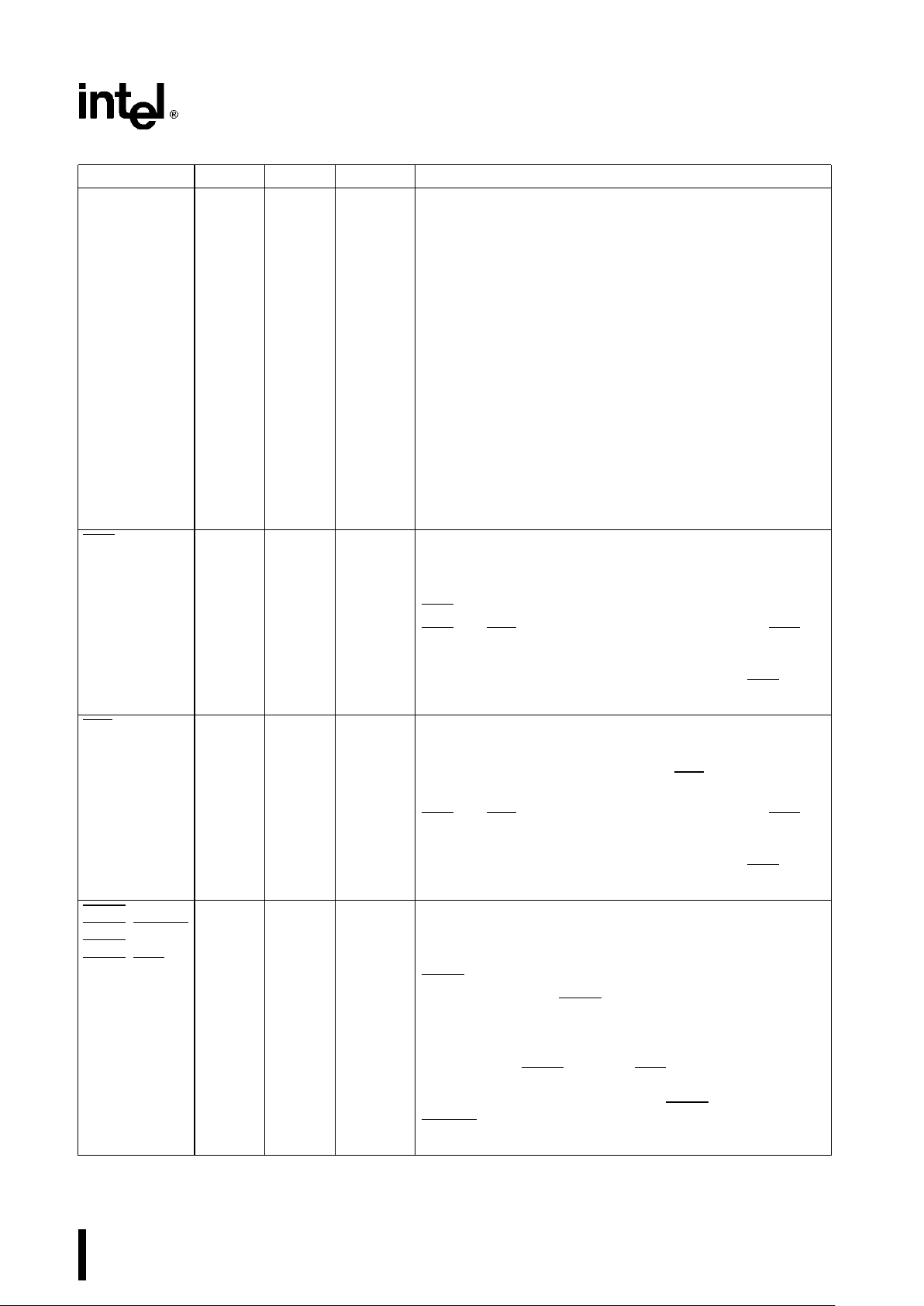
HLDA (output)
HOLD (input)
51
50
27
28
O
I HOLD indicates that another bus master is requesting the
local bus. The HOLD input is active HIGH. HOLD may be
asynchronous with respect to the M80C186 clock. The
M80C186 will issue a HLDA (HIGH) in response to a HOLD
request at the end of T
4
or Ti. Simultaneous with the
issuance of HLDA, the M80C186 will float the local bus and
control lines. After HOLD is detected as being LOW, the
M80C186 will lower HLDA. When the M80C186 needs to
run another bus cycle, it will again drive the local bus and
control lines.
In Enhanced Mode, HLDA will go low when a DRAM
refresh cycle is pending in the M80C186 and an external
bus master has control of the bus. It will be up to the
external master to relinquish the bus by lowering HOLD so
that the M80C186 may execute the refresh cycle. Lowering
HOLD for four clocks and returning HIGH will insure only
one refresh cycle to the external master. HLDA will
immediately go active after the refresh cycle has taken
place.
UCS 34 44 O Upper Memory Chip Select is an active LOW output
whenever a memory reference is made to the defined
upper portion (1K– 256K block) of memory. This line is not
floated during bus HOLD. The address range activating
UCS
is software programmable.
UCS and LCS are sampled upon the rising edge of RES.If
both pins are held low, the M80C186 will enter ONCE
Mode. In ONCE Mode all pins assume a high impedance
state and remain so until a subsequent RESET. UCS
has a
weak internal pullup for normal operation.
LCS 33 45 O Lower Memory Chip Select is active LOW whenever a
memory reference is made to the defined lower portion
(1K– 256K) of memory. This line is not floated during bus
HOLD. The address range activating LCS
is software
programmable.
UCS
and LCS are sampled upon the rising edge of RES.If
both pins are held low, the M80C186 will enter ONCE
Mode. In ONCE Mode all pins assume a high impedance
state and remain so until a subsequent RESET. UCS
has a
weak internal pullup for normal operation.
MCS0/PEREQ 38 40 I/O Mid-Range Memory Chip Select signals are active LOW
MCS1
/ERROR 37 41 I/O when a memory reference is made to the defined mid-
MCS2
36 42 O range portion of memory (8K – 512K). These lines are not
MCS3
/NPS 35 43 O floated during bus HOLD. The address ranges activating
MCS0
–3 are software programmable.
In Enhanced Mode, MCS0 becomes a PEREQ input
(Processor Extension Request). When connected to the
Numerics Processor Extension, this input is used to signal
the M80C186 when to make numeric data transfers to and
from the NPX. MCS3 becomes NPS (Numeric Processor
Select) which may only be activated by communication to
the Numerics Processor Extension. MCS1
becomes
ERROR in enhanced mode and is used to signal numerics
coprocessor errors.
7
M80C186
Table 1. M80C186 Pin Description (Continued)
Symbol PGA QFP Type Name and Function
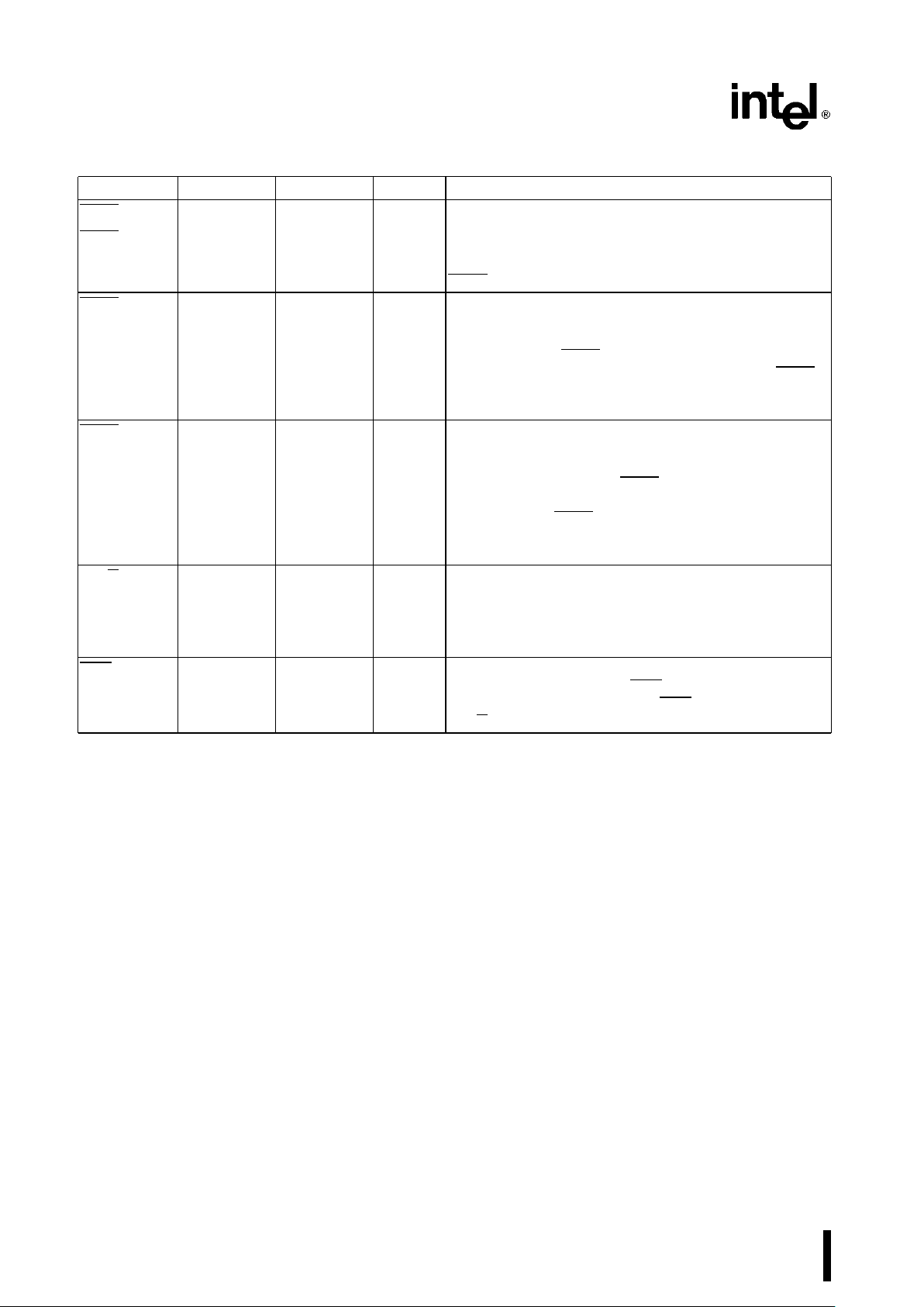
PCS0
PCS1–4 27, 28, 29, 302551, 50, 49, 48
53
O
O Peripheral Chip Select signals 0 –4 are active LOW
when a reference is made to the defined peripheral
area (64K byte I/O space). These lines are not floated
during bus HOLD. The address ranges activating
PCS0
–4 are software programmable.
PCS5/A1 31 47 O Peripheral Chip Select 5 or Latched A1 may be
programmed to provide a sixth peripheral chip select, or
to provide an internally latched A1 signal. The address
range activating PCS5
is software programmable. When
programmed to provide latched. A1, rather than PCS5
,
this pin will retain the previously latched value of A1
during a bus HOLD. A1 is active HIGH.
PCS6/A2 32 46 O Peripheral Chip Select 6 or Latched A2 may be
programmed to provide a seventh peripheral chip
select, or to provide an internally latched A2 signal. The
address range activating PCS6
is software
programmable. When programmed to provide latched
A2, rather than PCS6
, this pin will retain the previously
latched value of A2 during a bus HOLD. A2 is active
HIGH.
DT/R 40 38 O Data Transmit/Receive controls the direction of data
flow through the external M8286/M8287 data bus
transceiver. When LOW, data is transferred to the
M80C186. When HIGH the M80C186 places write data
on the data bus.
DEN 39 39 O Data Enable is provided as an M8286/M8287 data bus
transceiver output enable. DEN
is active LOW during
each memory and I/O access. DEN
is HIGH whenever
DT/R
changes state.
8

M80C186
FUNCTIONAL DESCRIPTION
Introduction
The following Functional Description describes the
base architecture of the M80C186. This architecture
is common to the M8086, M8088, M80186 and
M80286 microprocessor families as well. The
M80C186 is a very high integration 16-bit microprocessor. It combines 15 –20 of the most common microprocessor system components onto one chip.
The M80C186 is object code compatible with the
M8086/M8088 microprocessors and adds 10 new
instruction types to the existing M8086/M8088 instruction set.
The M80C186 has two major modes of operation,
Compatible and Enhanced. In Compatible Mode the
M80C186 is completely compatible with NMOS
M80186, with the exception of M8087 support. All
pin functions, timings, and drive capabilities are
identical. The Enhanced mode adds three new features to the system design. These are Power-Save
control, Dynamic RAM refresh, and an asynchronous Numerics Co-processor interface.
M80C186 BASE ARCHITECTURE
The M8086, M8088, M80186, and M80286 family all
contain the same basic set of registers, instructions,
and addressing modes. The M80C186 processor is
upward compatible with the M8086, M8088, and
M80286 CPUs.
Register Set
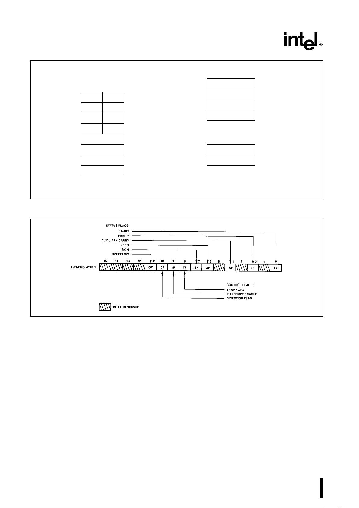
The M80C186 base architecture has fourteen registers as shown in Figures 3a and 3b. These registers
are grouped into the following categories.
General Registers
Eight 16-bit general purpose registers may be used
to contain arithmetic and logical operands. Four of
these (AX, BX, CX, and DX) can be used as 16-bit
registers or split into pairs of separate 8-bit registers.
Segment Registers
Four 16-bit special purpose registers select, at any
given time, the segments of memory that are immediately addressable for code, stack, and data. (For
usage, refer to Memory Organization.)
Base and Index Registers
Four of the general purpose registers may also be
used to determine offset addresses of operands in
memory. These registers may contain base addresses or indexes to particular locations within a segment. The addressing mode selects the specific registers for operand and address calculations.
Status and Control Registers
Two 16-bit special purpose registers record or alter
certain aspects of the M80C186 processor state.
These are the Instruction Pointer Register, which
contains the offset address of the next sequential
instruction to be executed, and the Status Word
Register, which contains status and control flag bits
(see Figures 3a and 3b).
Status Word Description
The Status Word records specific characteristics of
the result of logical and arithmetic instructions (bits
0, 2, 4, 6, 7, and 11) and controls the operation of
the M80C186 within a given operating mode (bits 8,
9, and 10). The Status Word Register is 16-bits wide.
The function of the Status Word bits is shown in
Table 2.
9
M80C186
16-BIT SPECIAL
REGISTER REGISTER
NAME FUNCTIONS
7070
BYTE
ADDRESSABLE
AX AH AL
MULTIPLY/DIVIDE
REGISTER
(8-BIT
DX DH DL
I/O INSTRUCTIONS
*
SHOWN)
NAMES
CX CH CL
(
LOOP/SHIFT/REPEAT/COUNT
%
BX BH BL
BASE REGISTERS
BP
*
SI
INDEX REGISTERS
DI
*
SP
(
STACK POINTER
15 0
GENERAL
REGISTERS
15 0
CS CODE SEGMENT SELECTOR
DS DATA SEGMENT SELECTOR
SS STACK SEGMENT SELECTOR
ES EXTRA SEGMENT SELECTOR
SEGMENT REGISTERS
15 0
F STATUS WORD
IP INSTRUCTION POINTER
STATUS AND CONTROL
REGISTERS
Figure 3a. M80C186 Register Set
270500–4
Figure 3b. Status Word Format
10

M80C186
Table 2. Status Word Bit Functions
Bit
Name Function
Position
0 CF Carry FlagÐSet on high-order
bit carry or borrow; cleared
otherwise
2 PF Parity FlagÐSet if low-order 8
bits of result contain an even
number of 1-bits; cleared
otherwise
4 AF Set on carry from or borrow to
the low order four bits of AL;
cleared otherwise
6 ZF Zero FlagÐSet if result is zero;
cleared otherwise
7 SF Sign FlagÐSet equal to high-
order bit of result (0 if positive,
1 if negative)
8 TF Single Step FlagÐOnce set, a
single step interrupt occurs
after the next instruction
executes. TF is cleared by the
single step interrupt.
9 IF Interrupt-enable FlagÐWhen
set, maskable interrupts will
cause the CPU to transfer
control to an interrupt vector
specified location.
10 DF Direction FlagÐCauses string
instructions to auto decrement
the appropriate index register
when set. Clearing DF causes
auto increment.
11 OF Overflow FlagÐSet if the
signed result cannot be
expressed within the number
of bits in the destination
operand; cleared otherwise
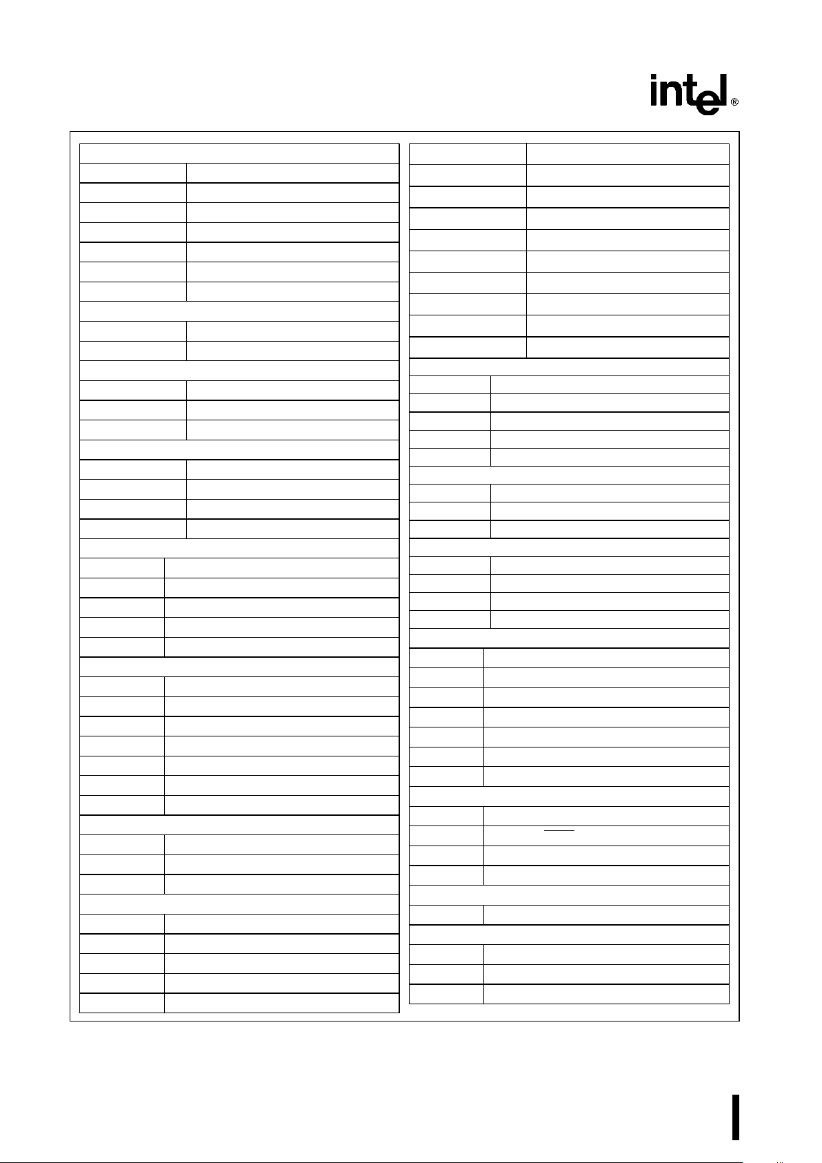
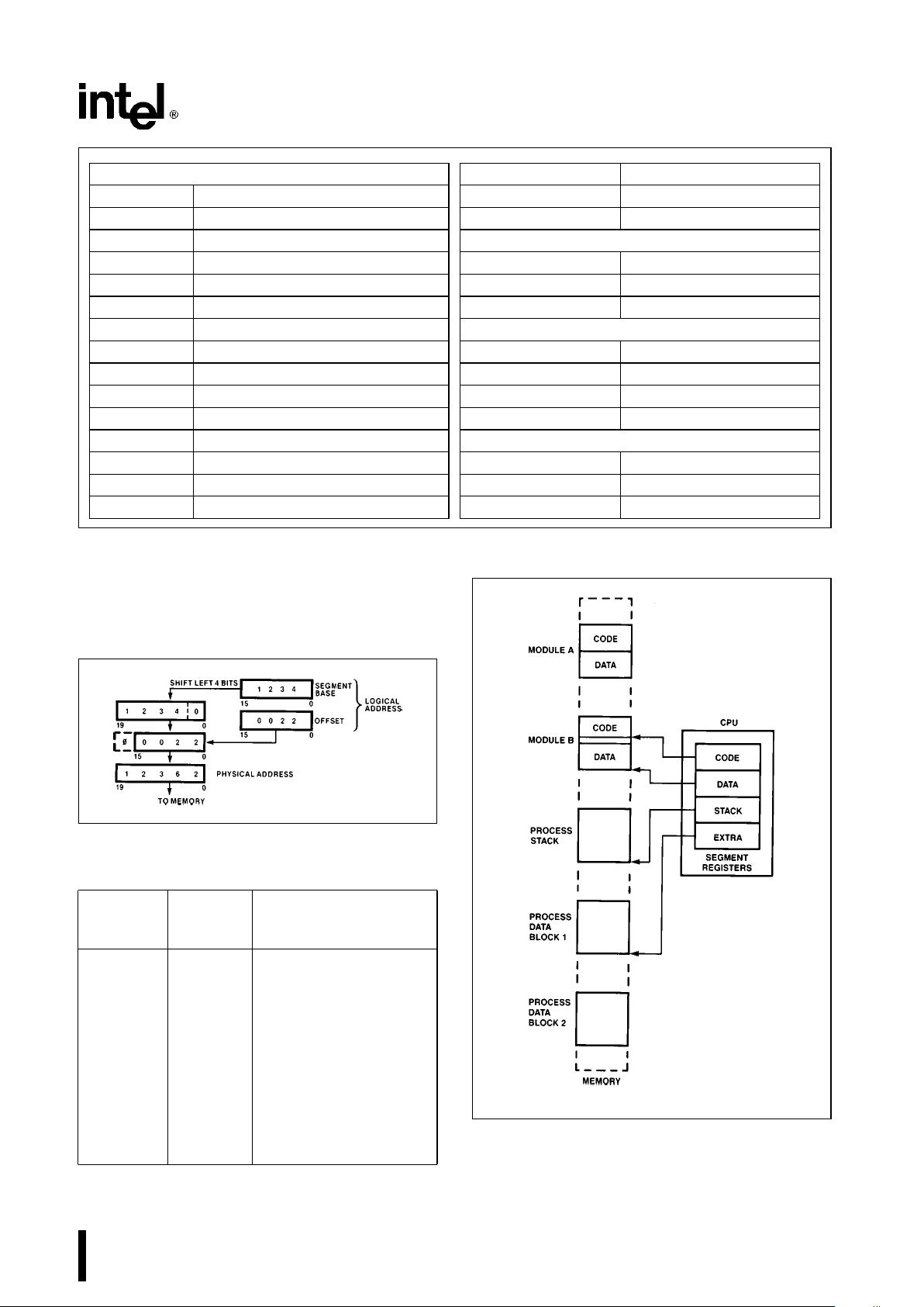
Instruction Set
The instruction set is divided into seven categories:
data transfer, arithmetic, shift/rotate/logical, string
manipulation, control transfer, high-level instructions, and processor control. These categories are
summarized in Figure 4.
An M80C186 instruction can reference anywhere
from zero to several operands. An operand can reside in a register, in the instruction itself, or in memory. Specific operand addressing modes are discussed later in this data sheet.
Memory Organization
Memory is organized in sets of segments. Each segment is a linear contiguous sequence of up to 64K
(2
16
) 8-bit bytes. Memory is addressed using a twocomponent address (a pointer) that consists of a 16bit base segment and a 16-bit offset. The 16-bit
base values are contained in one of four internal
segment register (code, data, stack, extra). The
physical address is calculated by shifting the base
value LEFT by four bits and adding the 16-bit offset
value to yield a 20-bit physical address (see Figure
5). This allows for a 1 MByte physical address size.
All instructions that address operands in memory
must specify the base segment and the 16-bit offset
value. For speed and compact instruction encoding,
the segment register used for physical address generation is implied by the addressing mode used (see
Table 3). These rules follow the way programs are
written (see Figure 6) as independent modules that
require areas for code and data, a stack, and access
to external data areas.
Special segment override instruction prefixes allow
the implicit segment register selection rules to be
overridden for special cases. The stack, data, and
extra segments may coincide for simple programs.
11
M80C186
GENERAL PURPOSE
MOV Move byte or word
PUSH Push word onto stack
POP Pop word off stack
PUSHA Push all registers on stack
POPA Pop all registers from stack
XCHG Exchange byte or word
XLAT Translate byte
INPUT/OUTPUT
IN Input byte or word
OUT Output byte or word
ADDRESS OBJECT
LEA Load effective address
LDS Load pointer using DS
LES Load pointer using ES
FLAG TRANSFER
LAHF Load AH register from flags
SAHF Store AH register in flags
PUSHF Push flags onto stack
POPF Pop flags off stack
ADDITION
ADD Add byte or word
ADC Add byte or word with carry
INC Increment byte or word by 1
AAA ASCII adjust for addition
DAA Decimal adjust for addition
SUBTRACTION
SUB Subtract byte or word
SBB Subtract byte or word with borrow
DEC Decrement byte or word by 1
NEG Negate byte or word
CMP Compare byte or word
AAS ASCII adjust for subtraction
DAS Decimal adjust for subtraction
MULTIPLICATION
MUL Multiply byte or word unsigned
IMUL Integer multiply byte or word
AAM ASCII adjust for multiplyASCII
DIVISION
DIV Divide byte or word unsigned
IDIV Integer divide byte or word
AAD ASCII adjust for division
CBW Convert byte to word
CWD Convert word to doubleword
MOVS Move byte or word string
INS Input bytes or word string
OUTS Output bytes or word string
CMPS Compare byte or word string
SCAS Scan byte or word string
LODS Load byte or word string
STOS Store byte or word string
REP Repeat
REPE/REPZ Repeat while equal/zero
REPNE/REPNZ Repeat while not equal/not zero
LOGICALS
NOT ‘‘Not’’ byte or word
AND ‘‘And’’ byte or word
OR ‘‘Inclusive or’’ byte or word
XOR ‘‘Exclusive or’’ byte or word
TEST ‘‘Test’’ byte or word
SHIFTS
SHL/SAL Shift logical/arithmetic left byte or word
SHR Shift logical right byte or word
SAR Shift arithmetic right byte or word
ROTATES
ROL Rotate left byte or word
ROR Rotate right byte or word
RCL Rotate through carry left byte or word
RCR Rotate through carry right byte or word
FLAG OPERATIONS
STC Set carry flag
CLC Clear carry flag
CMC Complement carry flag
STD Set direction flag
CLD Clear direction flag
STI Set interrupt enable flag
CLI Clear interrupt enable flag
EXTERNAL SYNCHRONIZATION
HLT Halt until interrupt or reset
WAIT Wait for TEST pin active
ESC Escape to extension processor
LOCK Lock bus during next instruction
NO OPERATION
NOP No operation
HIGH LEVEL INSTRUCTIONS
ENTER Format stack for procedure entry
LEAVE Restore stack for procedure exit
BOUND Detects values outside prescribed range
Figure 4. M80C186 Instruction Set
12
M80C186
CONDITIONAL TRANSFERS
JA/JNBE Jump if above/not below nor equal
JAE/JNB Jump if above or equal/not below
JB/JNAE Jump if below/not above nor equal
JBE/JNA Jump if below or equal/not above
JC Jump if carry
JE/JZ Jump if equal/zero
JG/JNLE Jump if greater/not less nor equal
JGE/JNL Jump if greater or equal/not less
JL/JNGE Jump if less/not greater nor equal
JLE/JNG Jump if less or equal/not greater
JNC Jump if not carry
JNE/JNZ Jump if not equal/not zero
JNO Jump if not overflow
JNP/JPO Jump if not parity/parity odd
JNS Jump if not sign
JO Jump if overflow
JP/JPE Jump if parity/parity even
JS Jump if sign
UNCONDITIONAL TRANSFERS
CALL Call procedure
RET Return from procedure
JMP Jump
ITERATION CONTROLS
LOOP Loop
LOOPE/LOOPZ Loop if equal/zero
LOOPNE/LOOPNZ Loop if not equal/not zero
JCXZ Jump if register CXe0
INTERRUPTS
INT Interrupt
INTO Interrupt if overflow
IRET Interrupt return
Figure 4. M80C186 Instruction Set (Continued)
To access operands that do not reside in one of the
four immediately available segments, a full 32-bit
pointer can be used to reload both the base (segment) and offset values.
270500–5
Figure 5. Two Component Address
Table 3. Segment Register Selection Rules
Memory Segment
Implicit Segment
Reference Register
Selection Rule
Needed Used
Instructions Code (CS) Instruction prefetch and
immediate data.
Stack Stack (SS) All stack pushes and
pops; any memory
references which use BP
Register as a base
register.
External Extra (ES) All string instruction
Data references which use
(Global) the DI register as an
index.
Local Data Data (DS) All other data references.
270500–6
Figure 6. Segmented Memory Helps
Structure Software
13

M80C186
Addressing Modes
The M80C186 provides eight categories of addressing modes to specify operands. Two addressing
modes are provided for instructions that operate on
register or immediate operands:
#
Register Operand Mode:
The operand is located
in one of the 8- or 16-bit general registers.
#
Immediate Operand Mode:
The operand is in-
cluded in the instruction.
Six modes are provided to specify the location of an
operand in a memory segment. A memory operand
address consists of two 16-bit components: a segment base and an offset. The segment base is supplied by a 16-bit segment register either implicitly
chosen by the addressing mode or explicitly chosen
by a segment override prefix. The offset, also called
the effective address, is calculated by summing any
combination of the following three address elements:
#
the
displacement
(an 8- or 16-bit immediate value
contained in the instruction);
#
the
base
(contents of either the BX or BP base
registers); and
#
the
index
(contents of either the SI or DI index
registers).
Any carry out from the 16-bit addition is ignored.
Eight-bit displacements are sign extended to 16-bit
values.
Combinations of these three address elements define the six memory addressing modes, described
below.
#
Direct Mode:
The operand’s offset is contained in
the instruction as an 8- or 16-bit displacement element.
#
Register Indirect Mode:
The operand’s offset is in
one of the registers SI, DI, BX, or BP.
#
Based Mode:
The operand’s offset is the sum of
an 8- or 16-bit displacement and the contents of
a base register (BX or BP).
#
Indexed Mode:
The operand’s offset is the sum
of an 8- or 16-bit displacement and the contents
of an index register (SI or DI).
#
Based Indexed Mode:
The operand’s offset is the
sum of the contents of a base register and an
Index register.
#
Based indexed Mode with Displacement:
The operand’s offset is the sum of a base register’s contents, an index register’s contents, and an 8- or
16-bit displacement.
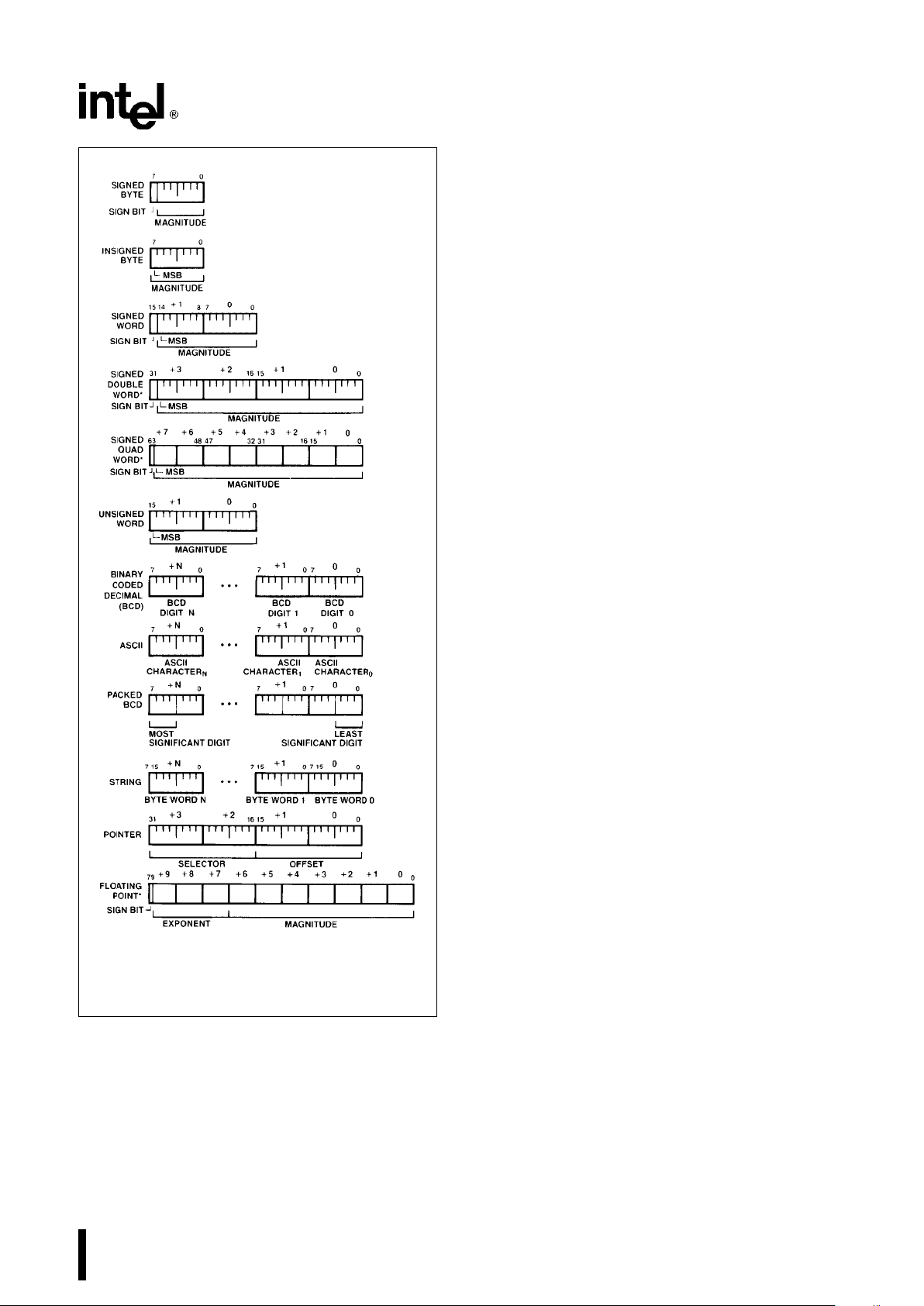
Data Types
The M80C186 directly supports the following data
types:
#
Integer:
A signed binary numeric value contained
in an 8-bit byte or a 16-bit word. All operations
assume a 2’s complement representation.
Signed 32- and 64-bit integers are supported using a Numeric Data Coprocessor with the
M80C186.
#
Ordinal:
An unsigned binary numeric value con-
tained in an 8-bit byte or a 16-bit word.
#
Pointer:
A 16- or 32-bit quantity, composed of a
16-bit offset component or a 16-bit segment base
component in addition to a 16-bit offset component.
#
String:
A contiguous sequence of bytes or words.
A string may contain from 1 to 64K bytes.
#
ASCII:
A byte representation of alphanumeric and
control characters using the ASCII standard of
character representation.
#
BCD:
A byte (unpacked) representation of the
decimal digits 0 – 9.
#
Packed BCD:
A byte (packed) representation of
two decimal digits (0– 9). One digit is stored in
each nibble (4-bits) of the byte.
#
Floating Point:
A signed 32-, 64-, or 80-bit real
number representation. (Floating point operands
are supported using a Numeric Data Coprocessor
with the M80C186.)
In general, individual data elements must fit within
defined segment limits. Figure 7 graphically represents the data types supported by the M80C186.
I/O Space
The I/O space consists of 64K 8-bit or 32K 16-bit
ports. Separate instructions address the I/O space
with either an 8-bit port address, specified in the instruction, or a 16-bit port address in the DX register.
8-bit port addresses are zero extended such that
A
15–A8
are LOW. I/O port addresses 00F8(H)
through 00FF(H) are reserved.
Interrupts
An interrupt transfers execution to a new program
location. The old program address (CS:IP) and machine state (Status Word) are saved on the stack to
allow resumption of the interrupted program. Interrupts fall into three classes: hardware initiated, INT
instructions, and instruction exceptions. Hardware
initiated interrupts occur in response to an external
input and are classified as non-maskable or maskable.
14
M80C186
270500–7
NOTE:
*Supported by using a Numeric Data Coprocessor with
the M80C186.
Figure 7. M80C186 Supported Data Types
Programs may cause an interrupt with an INT instruction. Instruction exceptions occur when an unusual condition, which prevents further instruction
processing, is detected while attempting to execute
an instruction. If the exception was caused by executing an ESC instruction with the ESC trap bit set in
the relocation register, the return instruction will
point to the ESC instruction, or to the segment override prefix immediately preceding the ESC instruc-
tion if the prefix was present. In all other cases, the
return address from an exception will point at the
instruction immediately following the instruction
causing the exception.
A table containing up to 256 pointers defines the
proper interrupt service routine for each interrupt. Interrupts 0– 31, some of which are used for instruction exceptions, are reserved. Table 4 shows the
M80C186 predefined types and default priority levels. For each interrupt, an 8-bit vector must be supplied to the M80C186 which identifies the appropriate table entry. Exceptions supply the interrupt
vector internally. In addition, internal peripherals and
noncascaded external interrupts will generate their
own vectors through the internal interrupt controller.
INT instructions contain or imply the vector and allow access to all 256 interrupts. Maskable hardware
initiated interrupts supply the 8-bit vector to the CPU
during an interrupt acknowledge bus sequence.
Non-maskable hardware interrupts use a predefined
internally supplied vector.
Interrupt Sources
The M80C186 can service interrupts generated by
software or hardware. The software interrupts are
generated by specific instructions (INT, ESC, unused
OP, etc.) or the results of conditions specified by
instructions (array bounds check, INT0, DIV, IDIV,
etc.). All interrupt sources are serviced by an indirect
call through an element of a vector table. This vector
table is indexed by using the interrupt vector type
(Table 4), multiplied by four. All hardware-generated
interrupts are sampled at the end of each instruction. Thus, the software interrupts will begin service
first. Once the service routine is entered and interrupts are enabled, any hardware source of sufficient
priority can interrupt the service routine in progress.
The software generated M80C186 interrupts are described below.
DIVIDE ERROR EXCEPTION (TYPE 0)
Generated when a DIV or IDIV instruction quotient
cannot be expressed in the number of bits in the
destination.
SINGLE-STEP INTERRUPT (TYPE 1)
Generated after most instructions if the TF flag is
set. Interrupts will not be generated after prefix instructions (e.g., REP), instructions which modify segment registers (e.g., POP DS), or the WAIT instruction.
NON-MASKABLE INTERRUPTÐNMI (TYPE 2)
An external interrupt source which cannot be
masked.
15
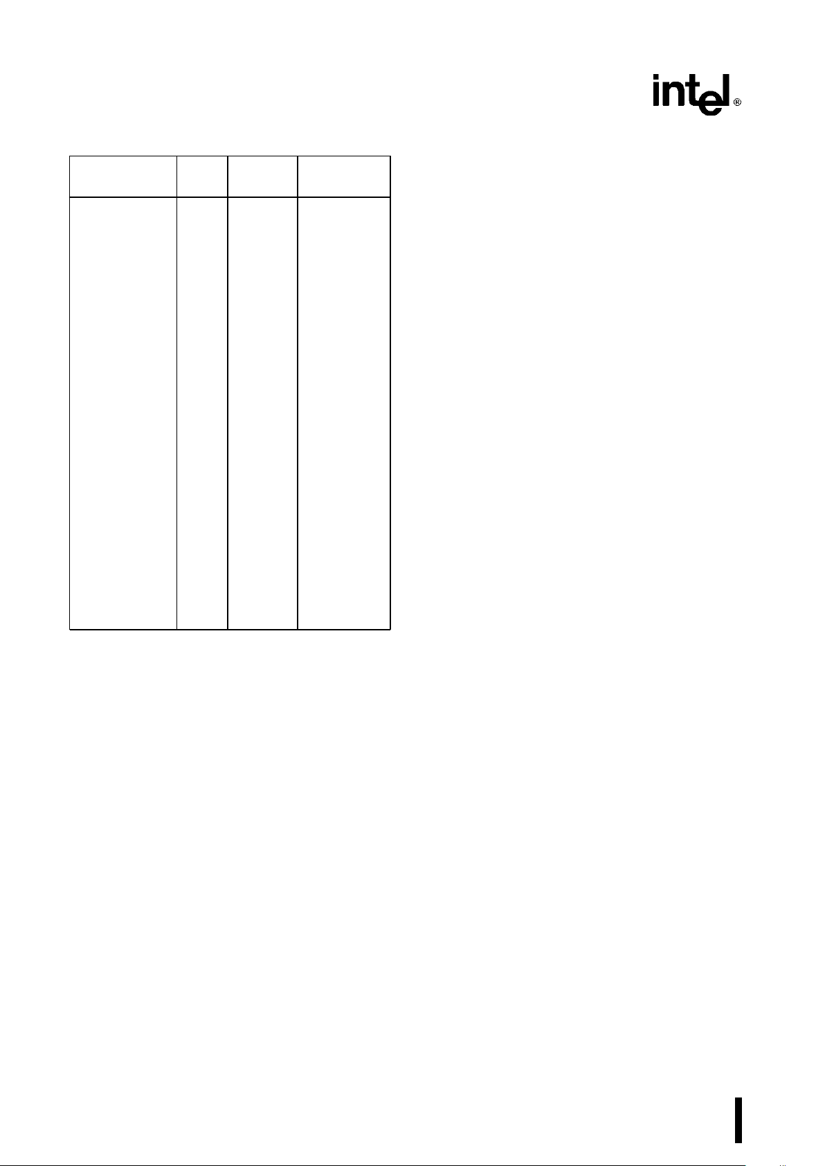
M80C186
Table 4. M80C186 Interrupt Vectors
Interrupt Vector Default Related
Name Type Priority
(4)
Instructions
Divide Error 0 1
(1)
DIV, IDIV
Exception
Single Step 1 12
(2)
All
Interrupt
NMI 2 1 All
Breakpoint 3 1
(1)
INT
Interrupt
INT0 Detected 4 1
(1)
INT0
Overflow
Exception
Array Bounds 5 1
(1)
BOUND
Exception
Unused-Opcode 6 1
(1)
Undefined
Exception Opcodes
ESC Opcode 7 1
(1), (5)
ESC Opcodes
Exception
Timer 0 Interrupt 8 2A
(3)
Timer 1 Interrupt 18 2B
(3)
Timer 2 Interrupt 19 2C
(3)
Reserved 9 3
DMA 0 Interrupt 10 4
DMA 1 Interrupt 11 5
INT0 Interrupt 12 6
INT1 Interrupt 13 7
INT2 Interrupt 14 8
INT3 Interrupt 15 9
NOTES:
1. These are generated as the result of an instruction execution.
2. This is handled as in the M8086.
3. All three timers constitute one source of request to the
interrupt controller. The Timer interrupts all have the same
default priority level with respect to all other interrupt
sources. However, they have a defined priority ordering
amongst themselves. (Priority 2A is higher priority than 2B.)
Each Timer interrupt has a separate vector type number.
4. Default priorities for the interrupt sources are used only if
the user does not program each source into a unique priority level.
5. An escape opcode will cause a trap if the M80C186 is in
compatible mode or if the processor is in enhanced mode
with the proper bit set in the peripheral control block relocation register.
BREAKPOINT INTERRUPT (TYPE 3)
A one-byte version of the INT instruction. It uses 12
as an index into the service routine address table
(because it is a type 3 interrupt).
INT0 DETECTED OVERFLOW EXCEPTION
(TYPE4)
Generated during an INT0 instruction if the 0F bit is
set.
ARRAY BOUNDS EXCEPTION (TYPE 5)
Generated during a BOUND instruction if the array
index is outside the array bounds. The array bounds
are located in memory at a location indicated by one
of the instruction operands. The other operand indicates the value of the index to be checked.
UNUSED OPCODE EXCEPTION (TYPE 6)
Generated if execution is attempted on undefined
opcodes.
ESCAPE OPCODE EXCEPTION (TYPE 7)
Generated if execution is attempted of ESC opcodes
(D8H– DFH). In compatible mode operation, ESC
opcodes will always generate this exception. In enhanced mode operation, the exception will be generated only if a bit in the relocation register is set. The
return address of this exception will point to the ESC
instruction causing the exception. If a segment override prefix preceded the ESC instruction, the return
address will point to the segment override prefix.
Hardware-generated interrupts are divided into two
groups: maskable interrupts and non-maskable interrupts. The M80C186 provides maskable hardware
interrupt request pins INT0 –INT3. In addition, maskable interrupts may be generated by the M80C186
integrated DMA controller and the integrated timer
unit. The vector types for these interrupts is shown
in Table 4. Software enables these inputs by setting
the interrupt flag bit (IF) in the Status Word. The interrupt controller is discussed in the peripheral section of this data sheet.
Further maskable interrupts are disabled while servicing an interrupt because the IF bit is reset as part
of the response to an interrupt or exception. The
saved Status Word will reflect the enable status of
the processor prior to the interrupt. The interrupt flag
will remain zero unless specifically set. The interrupt
return instruction restores the Status Word, thereby
restoring the original status of IF bit. If the interrupt
return re-enables interrupts, and another interrupt is
pending, the M80C186 will immediately service the
highest-priority interrupt pending, i.e., no instructions
of the main line program will be executed.
Non-Maskable Interrupt Request (NMI)
A non-maskable interrupt (NMI) is also provided.
This interrupt is serviced regardless of the state of
the IF bit. A typical use of NMI would be to activate a
power failure routine. The activation of this input
causes an interrupt with an internally supplied vector
value of 2. No external interrupt acknowledge sequence is performed. The IF bit is cleared at the
beginning of an NMI interrupt to prevent maskable
interrupts from being serviced.
16

M80C186
Single-Step Interrupt
The M80C186 has an internal interrupt that allows
programs to execute one instruction at a time. It is
called the single-step interrupt and is controlled by
the single-step flag bit (TF) in the Status Word. Once
this bit is set, an internal single-step interrupt will
occur after the next instruction has been executed.
The interrupt clears the TF bit and uses an internally
supplied vector of 1. The IRET instruction is used to
set the TF bit and transfer control to the next instruction to be single-stepped.
Initialization and Processor Reset
Processor initialization or startup is accomplished by
driving the RES
input pin LOW. RES forces the
M80C186 to terminate all execution and local bus
activity. No instruction or bus activity will occur as
long as RES
is active. After RES becomes inactive
and an internal processing interval elapses, the
M80C186 begins execution with the instruction at
physical location FFFF0(H). RES
also sets some
registers to predefined values as shown in Table 5.
Table 5. M80C186 Initial Register State
after RESET
Status Word F002(H)
Instruction Pointer 0000(H)
Code Segment FFFF(H)
Data Segment 0000(H)
Extra Segment 0000(H)
Stack Segment 0000(H)
Relocation Register 20FF(H)
UMCS FFFB(H)
M80C186 CLOCK GENERATOR
The M80C186 provides an on-chip clock generator
for both internal and external clock generation. The
clock generator features a crystal oscillator, a divideby-two counter, synchronous and asynchronous
ready inputs, and reset circuitry.
Oscillator
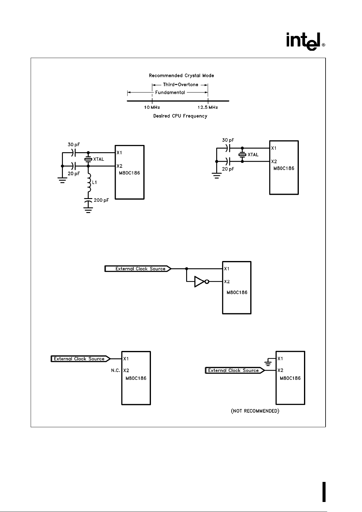
The M80C186 oscillator circuit is designed to be
used with either a parallel resonant fundamental or
third-overtone mode crystal, depending upon the
frequency range of the application as shown in Figure 8a. This is used as the time base for the
M80C186. The crystal frequency chosen should be
twice the required processor frequency. Use of an
LC or RC circuit is not recommended.
The oscillator output is not directly available external
to the M80C186. The two recommended crys-
tal configurations are shown in Figures 8b and 8c.
When used in third-overtone mode the tank circuit
shown in Figure 8b is recommended for stable operation. The sum of the stray capacitances and loading capacitors should equal the values shown. It is
advisable to limit stray capacitance between the X1
and X2 pins to less than 10 pF. While a fundamental-mode circuit will require approximately 1 ms for
start-up, the third-overtone arrangement may require
1 ms to 3 ms to stabilize.
Alternately the oscillator pins may be driven from an
external source as shown in Figure 8d or Figure 8e.
The configuration shown in Figure 8f is not recommended.
The following parameters may be used for choosing
a crystal:
Temperature Range:
b
55§Ctoa125§C
ESR (Equivalent Series Resistance): 40X max
C
0
(Shunt Capacitance of Crystal): 7.0 pf max
C
1
(Load Capacitance): 20 pFg2pF
Drive Level: 1 mW max
Clock Generator
The M80C186 clock generator provides the 50%
duty cycle processor clock for the M80C186. It does
this by dividing the oscillator output by 2 forming the
symmetrical clock. If an external oscillator is used,
the state of the clock generator will change on the
falling edge of the oscillator signal. The CLKOUT pin
provides the processor clock signal for use outside
the M80C186. This may be used to drive other system components. All timings are referenced to the
output clock.
READY Synchronization
The M80C186 provides both synchronous and asynchronous ready inputs. Asynchronous ready synchronization is accomplished by circuitry which samples ARDY in the middle of T
2,T3
and again in the
middle of each T
W
until ARDY is sampled HIGH.
One-half CLKOUT cycle of resolution time is used.
Full synchronization is performed only on the rising
edge of ARDY, i.e., the falling edge of ARDY must
be synchronized to the CLKOUT signal if it will occur
during T
2,T3
,orTW. High-to-LOW transitions of
ARDY must be performed synchronously to the CPU
clock.
A second ready input (SRDY) is provided to interface with externally synchronized ready signals. This
input is sampled at the end of T
2,T3
and again at
the end of each T
W
until it is sampled HIGH. By
using this input rather than the asynchronous ready
input, the half-clock cycle resolution time penalty is
eliminated.
17
M80C186
270500–8
(8a)
270500–25
(8b)
(8c)
270500–24
Note 1:
XTAL Frequency L1 Value
20 Mhz 12.0 mH
g
20%
25 Mhz 8.2 mH
g
20%
(8d)
270500–26
(8e)
270500–27
(8f)
270500–28
Figure 8. M80C186 Oscillator Configurations
18
 Loading...