Intel Corporation KU80C51SL-AH, KU87C51SL-AH, KU83C51SL-AH, KU81C51SL-AH, SB80C51SL-AL Datasheet
...
*Other brands and names are the property of their respective owners.
Information in this document is provided in connection with Intel products. Intel assumes no liability whatsoever, including infringement of any patent or
copyright, for sale and use of Intel products except as provided in Intel’s Terms and Conditions of Sale for such products. Intel retains the right to make
changes to these specifications at any time, without notice. Microcomputer Products may have minor variations to this specification known as errata.
November 1994COPYRIGHT©INTEL CORPORATION, 1995 Order Number: 272271-002
8XC51SL/LOW VOLTAGE 8XC51SL
KEYBOARD CONTROLLER
80C51SL Ð CPU with RAM and I/O; V
CC
e
5Vg10%
81C51SL Ð 16K ROM Preprogrammed with SystemSoft Keyboard Controller and Scanner
Firmware. V
CC
e
5Vg10%.
83C51SL Ð 16K Factory Programmed ROM. V
CC
e
5Vg10%.
87C51SL Ð 16K OTP ROM. V
CC
e
5Vg10%.
Low Voltage 80C51SLÐCPU with RAM and I/O; V
CC
e
3.3Vg0.3V
Low Voltage 81C51SLÐ 16K ROM Preprogrammed with SystemSoft Keyboard Controller
and Scanner Firmware. V
CC
e
3.3Vg0.3V.
Low Voltage 83C51SLÐ 16K Factory Programmed ROM. V
CC
e
3.3Vg0.3V.
Low Voltage 87C51SLÐ 16K OTP ROM. V
CC
e
3.3Vg0.3V.
Y
Proliferation of 8051 Architecture
Y
Complete 8042 Keyboard Control
Functionality
Y
8042 Style Host Interface
Y
Optional Hardware Speedup of
GATEA20 and RCL
Y
Local 16 x 8 Keyboard Switch Matrix
Support
Y
Two Industry Standard Serial Keyboard
Interfaces; Supported via Four High
Drive Outputs
Y
5 LED Drivers
Y
Low Power CHMOS Technology
Y
4-Channel, 8-Bit A/D
Y
Interface for up to 32 Kbytes of
External Memory
Y
Slew Rate Controlled I/O Buffers Used
to Minimize Noise
Y
256 Bytes Data RAM
Y
Three Multifunction I/O Ports
Y
10 Interrupt Sources with 6 UserDefinable External Interrupts
Y
2 MHz – 16 MHz Clock Frequency
Y
100-Pin PQFP (8XC51SL)
100-Pin SQFP (Low Voltage 8XC51SL)
The 8XC51SL, based on Intel’s industry-standard MCSÉ51 microcontroller family, is designed for keyboard
control in laptop and notebook PCs. The highly integrated keyboard controller incorporates an 8042-style UPI
host interface with expanded memory, keyboard scan, and power management. The 8XC51SL supports both
serial and scanned keyboard interfaces and is available in pre-programmed versions to reduce time to market.
The Low Voltage 8XC51SL is the 3.3V version optimized for even further power savings. Throughout the
remainder of this document, both devices will generally be referred to as 51SL.
The 8XC51SL is a pin-for-pin compatible replacement for the 8XC51SL-BG. It does, however have some
additional functionality. Those additional functions are as follows:
1. 16K OTP ROM: The 8XC51SL-BG had only 8K of ROM.
2. New Register Set: The 8XC51SL adds a second set of host interface registers available for use in supporting power management. This required an additional address line (A1) for decoding. To accommodate this,
one V
CC
pin was removed. However, in order to maintain compatibility with the -BG version, an enable bit
for this new register set was added in configuration register 1. This allows the 8XC51SL to be drop in
compatible to existing 8XC51SL-BG designs; no software modifications required.
NOTE:
The changes made to the V
CC
pins require that all three VCCpins be properly connected. Failing to do so
could result in high leakage current and possible damage to the device.
8XC51SL/LOW VOLTAGE 8XC51SL
272271– 1
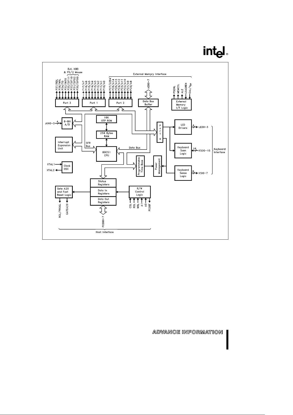
Figure 1. Block Diagram
2
8XC51SL/LOW VOLTAGE 8XC51SL
272271– 2
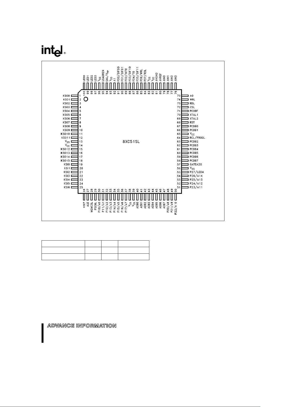
Figure 2. Connection Diagram (PQFP and SQFP)
PACKAGES
Part Prefix Suffix Package Type
8XC51SL KU AH 100-Pin PQFP
Low Voltage 8XC51SL SB AL 100-Pin SQFP
3
8XC51SL/LOW VOLTAGE 8XC51SL
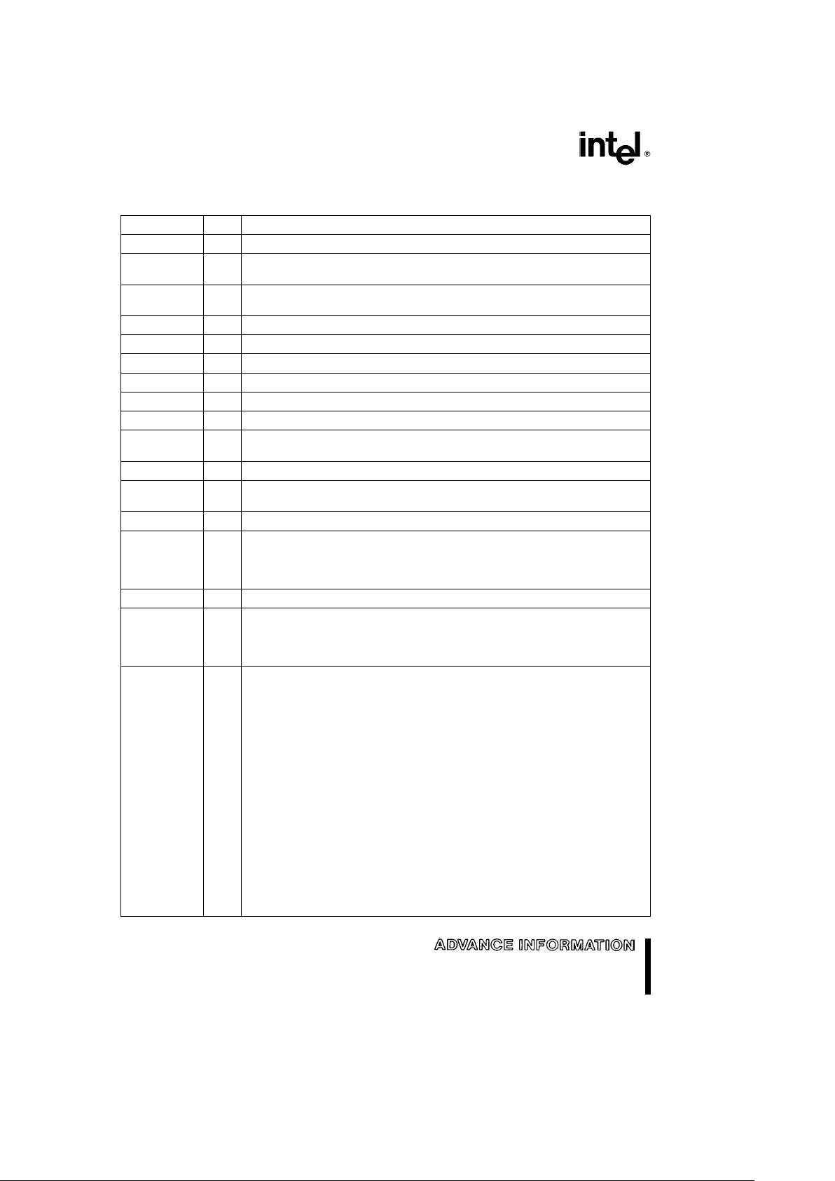
PIN DESCRIPTIONS
Table 1. Pin Descriptions
Symbol Type Description
V
SS
Circuit ground potential.
V
CC
Supply voltage during normal, Idle, and Power-Down operation; nominallya5V
g
10% for 8XC51SL,a3.3Vg0.3V for Low Voltage 8XC51SL.
PCDB0–7 I/O Host interface data bus. An 8-bit bidirectional port for data transfers between the
host processor and the keyboard controller.
WRL I The active-low, host-interface write signal.
RDL I The active-low, host-interface read signal.
CSL I The active-low, host-interface chip select.
A0–A1 I Host-Interface Address select inputs.
PCOBF O The active-high, host-interface Output Buffer Full interrupt.
GATEA20 O Gate A20 control signal output.
RCL/PROGL O Host resetÐactive low. This pin is also the program pulse input during EPROM
programming.
LED0–3 O LED output drivers.
KSI0–7 I Keyboard input scan lines (input Port 0). Schmitt inputs with 5K –20K pull-up
resistors.
KSO0–15 O Keyboard output scan lines.
PORT 1 I/O Port 1 is a general-purpose, 8-bit bidirectional port with internal pull-ups. It also
supports the following user-selectable functions:
P10/A0– P10–P16 are available for connection to dedicated keyboard inputs. A0 – A7 output
the low-order address byte (refer to LOADREN signal).
P17/A7
LOADREN I Low address enable. When set high, address bits A0 –A7 are output on P10–P17.
PORT2 I/O Port 2 is a general-purpose, 8-bit bidirectional port with internal pull-ups on P20 – 6/
A8–14. It also supports the following user-selectable functions:
P20–6/A8– 14 P20– 6/A8 – 14 output the high-order address byte.
P27/LED4 P27/LED4 is available as a fifth LED output driver (by writing to the port bit 7).
PORT 3 I/O Port 3 is a general-purpose, 8-bit bidirectional port. P32/INT0, P34/T0, P36/WRL,
and P37/RDL have internal pull-ups. P30/SIF00, P31/SIF01, P33/SIF10, and
P35/SIF11 are high-drive open-drain outputs. It also supports the following user-
selectable functions:
P30/SIF00 A high-drive, open-drain output to support an external serial keyboard interface
(typically CLK); RXD (8051 UART serial input port); SIF0INTL (serial interface
interrupt 0).
P31/SIF01 A high-drive, open-drain output to support an external serial keyboard interface
(typically DATA); TXD (8051 UART serial output port).
P32/INT0 INT0L (external interrupt 0).
P33/SIF10 A high-drive, open-drain output to support an external serial keyboard interface
(typically mouse CLK); SIF1INTL (external interrupt 1).
P34/T0 AUXOBF1 (output buffer fullÐmouse support); T0 (Timer/Counter 0 external
input).
P35/SIF11 A high-drive, open-drain output to support an external serial keyboard interface
(typically mouse DATA); T1 (Timer/Counter 1 external input).
P36/WRL WRL (external data memory write strobe); inactive at addresses 7FF0 – 7FFFH.
P37/RDL AUXOBF2 (output buffer full interrupt); INT2L (external interrupt); RDL (external
data memory read strobe); inactive at addresses 7FF0 – FFFFH.
4

8XC51SL/LOW VOLTAGE 8XC51SL
PIN DESCRIPTIONS (Continued)
Table 1. Pin Descriptions (Continued)
Symbol Type Description
XTAL1 I Input to the on-chip oscillator.
XTAL2 O Output from the on-chip oscillator.
AVGND Analog ground potential.
AVREF Analog supply voltage; nominallya5Vg10% for 8XC51SL,a3.3Vg0.3V for Low
Voltage 8XC51SL.
AIN0–3 I A/D Analog input channels.
ADB0–7 I/O External address/data bus. Multiplexes the low-address byte and data during external
memory accesses.
EAL/V
PP
I External address input. When held high, the 51SL CPU executes out of internal Program
Memory unless the program counter exceeds 3FFFH. When held low, the 51SL CPU
always executes out of external memory. EAL is latched on the falling edge of RST. This
pin also receives the programming supply voltage (V
PP
) during EPROM programming.
ALE O Address Latch Enable output pulse latches the low address byte during external
memory access. ALE is output at a constant rate of (/6 the oscillator frequency, whether
or not there are accesses to external memory. One ALE pulse is skipped during the
execution of a MOVX instruction. ALE is disabled during Idle mode and can also be
disabled via Configuration register 1 control.
PSENL O Program Store Enable is the read strobe to external program memory. PSENL is
qualified with RDL and A15 for use with an external Flash memory. PSENL is not active
when the device executes out of internal program memory.
MEMCSL I/O External Memory Chip Select for code space address 4000H and above, when EAL is
inactive (i.e., high). For EAL low, MEMCSL is active. Goes inactive during Idle mode and
Power-Down mode. If external memory interfacing is not required, MEMCSL can be
configured as a general purpose I/O (controlled via Configuration register 1).
RST I Resets the keyboard controller. Hold RST high for two machine cycles.
5
8XC51SL/LOW VOLTAGE 8XC51SL
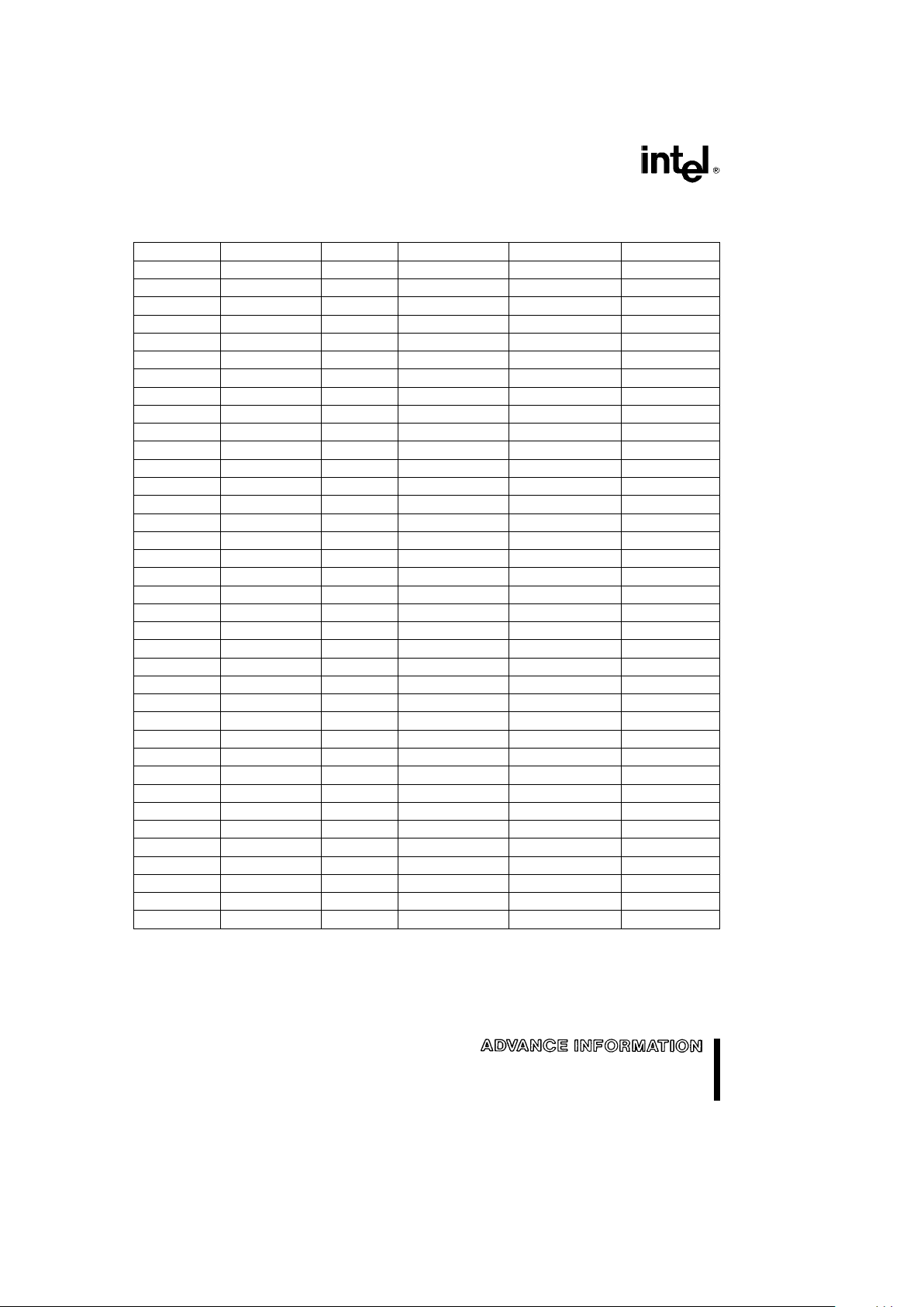
8XC51SL/LOW VOLTAGE 8XC51SL PIN CHARACTERISTICS
Table 2. Pin Characteristics
Pin No. Pin Name Type Term Reset PD Mode
1 KSO0 O OD TRI HOLD
2 KSO1 O OD TRI HOLD
3 KSO2 O OD TRI HOLD
4 KSO3 O OD TRI HOLD
5 KSO4 O OD TRI HOLD
6 KSO5 O OD TRI HOLD
7 KSO6 O OD TRI HOLD
8 KSO7 O OD TRI HOLD
9 KSO8 O OD TRI HOLD
10 KSO9 O OD TRI HOLD
11 KSO10 O OD TRI HOLD
12 KSO11 O OD TRI HOLD
13 V
SS
14 V
CC
15 KSO12 O OD TRI HOLD
16 KSO13 O OD TRI HOLD
17 KSO14 O OD TRI HOLD
18 KSO15 O OD L HOLD
19 KSI0 I 5K–20K PU NC
20 KSI1 I 5K–20K PU NC
21 KSI2 I 5K–20K PU NC
22 KSI3 I 5K–20K PU NC
23 KSI4 I 5K–20K PU NC
24 KSI5 I 5K–20K PU NC
25 KSI6 I 5K–20K PU NC
26 KSI7 I 5K–20K PU NC
27 ALE O L L
28 MEMCSL O L (EALe0) H
29 PSENL O L L
30 P10/A0 I/O PU WH HOLD
31 P11/A1 I/O PU WH HOLD
32 P12/A2 I/O PU WH HOLD
33 P13/A3 I/O PU WH HOLD
34 P14/A4 I/O PU WH HOLD
35 P15/A5 I/O PU WH HOLD
36 P16/A6 I/O PU WH HOLD
37 P17/A7 I/O PU WH HOLD
6
8XC51SL/LOW VOLTAGE 8XC51SL
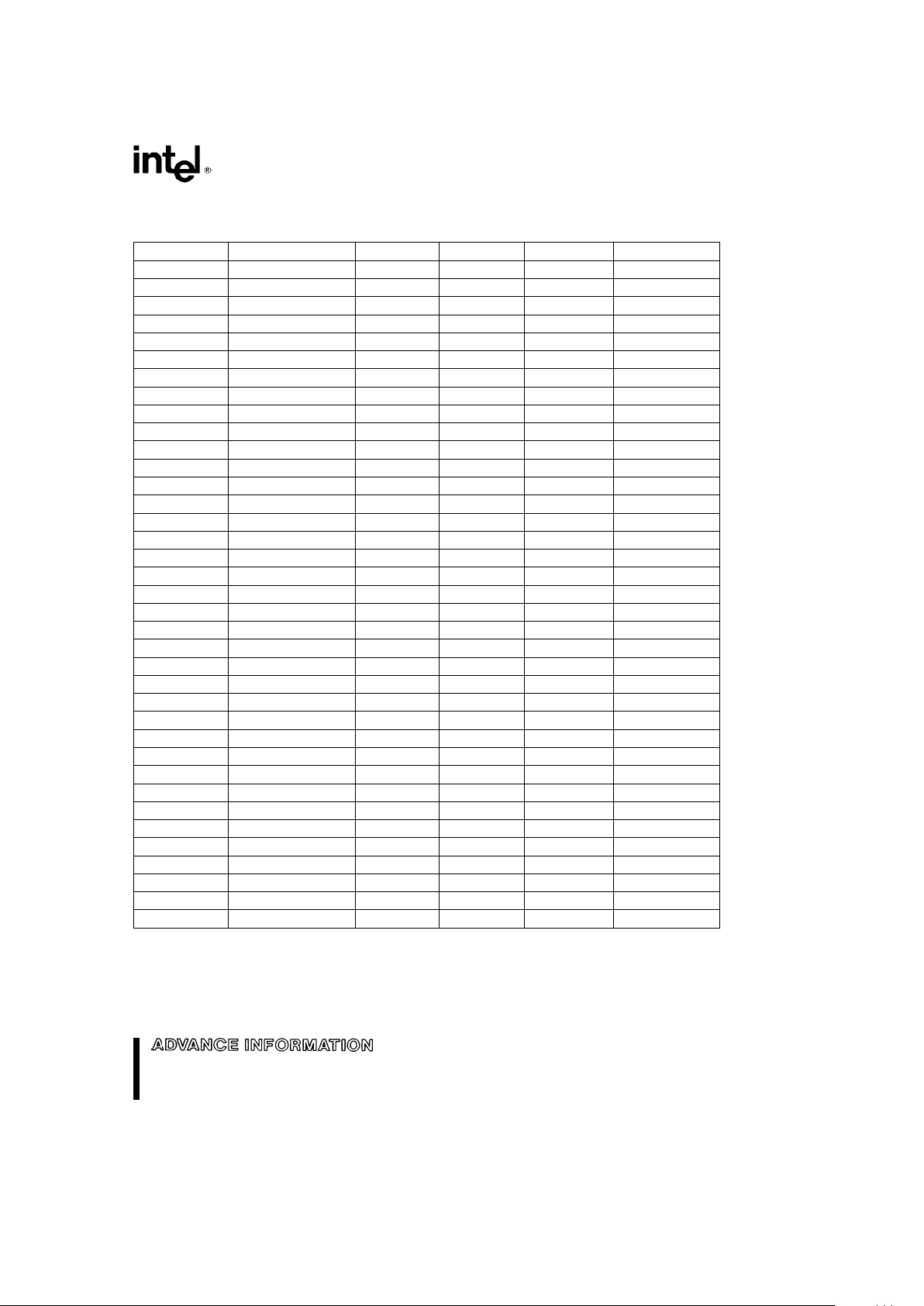
8XC51SL/LOW VOLTAGE 8XC51SL PIN CHARACTERISTICS (Continued)
Table 2. Pin Characteristics (Continued)
Pin No. Pin Name Type Term Reset PD Mode
38 V
SS
39 V
SS
40 ADB0 I/O TRI TRI
41 ADB1 I/O TRI TRI
42 ADB2 I/O TRI TRI
43 ADB3 I/O TRI TRI
44 ADB4 I/O TRI TRI
45 ADB5 I/O TRI TRI
46 ADB6 I/O TRI TRI
47 ADB7 I/O TRI TRI
48 P20/A8 I/O PU WH HOLD
49 P21/A9 I/O PU WH HOLD
50 P22/A10 I/O PU WH HOLD
51 P23/A11 I/O PU WH HOLD
52 P24/A12 I/O PU WH HOLD
53 P25/A13 I/O PU WH HOLD
54 P26/A14 I/O PU WH HOLD
55 P27/LED4 I/O OD TRI HOLD
56 V
SS
57 GATEA20 O WH HOLD
58 PCDB7 I/O TRI TRI
59 PCDB6 I/O TRI TRI
60 PCDB5 I/O TRI TRI
61 PCDB4 I/O TRI TRI
62 PCDB3 I/O TRI TRI
63 PCDB2 I/O TRI TRI
64 RCL/PROGL O WH HOLD
65 V
CC
66 PCDB1 I/O TRI TRI
67 PCDB0 I/O TRI TRI
68 RST I
69 XTAL2 O H
70 XTAL1 I
71 PCOBF O L HOLD
72 CSL I
73 RDL I
74 WRL I
7
 Loading...