Intel Corporation KU386SX Datasheet
*Other brands and names are the property of their respective owners.
Information in this document is provided in connection with Intel products. Intel assumes no liability whatsoever, including infringement of any patent or
copyright, for sale and use of Intel products except as provided in Intel’s Terms and Conditions of Sale for such products. Intel retains the right to make
changes to these specifications at any time, without notice. Microcomputer Products may have minor variations to this specification known as errata.
January 1994COPYRIGHT©INTEL CORPORATION, 1995 Order Number: 240187-008
Intel386TMSX MICROPROCESSOR
Y
Full 32-Bit Internal Architecture
Ð 8-, 16-, 32-Bit Data Types
Ð 8 General Purpose 32-Bit Registers
Y
Runs Intel386TMSoftware in a Cost
Effective 16-Bit Hardware Environment
Ð Runs Same Applications and O.S.’s
as the Intel386
TM
DX Processor
Ð Object Code Compatible with 8086,
80186, 80286, and Intel386
TM
Processors
Y
High Performance 16-Bit Data Bus
Ð 16, 20, 25 and 33 MHz Clock
Ð Two-Clock Bus Cycles
Ð Address Pipelining Allows Use of
Slower/Cheaper Memories
Y
Integrated Memory Management Unit
Ð Virtual Memory Support
Ð Optional On-Chip Paging
Ð 4 Levels of Hardware Enforced
Protection
Ð MMU Fully Compatible with Those of
the 80286 and Intel386 DX CPUs
Y
Virtual 8086 Mode Allows Execution of
8086 Software in a Protected and
Paged System
Y
Large Uniform Address Space
Ð 16 Megabyte Physical
Ð 64 Terabyte Virtual
Ð 4 Gigabyte Maximum Segment Size
Y
Numerics Support with the Intel387
TM
SX Math CoProcessor
Y
On-Chip Debugging Support Including
Breakpoint Registers
Y
Complete System Development
Support
Ð Software: C, PL/M, Assembler
Ð Debuggers: PMON-386 DX,
ICE
TM
-386 SX
Y
High Speed CHMOS IV Technology
Y
Operating Frequency:
Ð Standard
(Intel386 SX -33, -25, -20, -16)
Min/Max Frequency
(4/33, 4/25, 4/20, 4/16) MHz
Ð Low Power
(Intel386 SX -33, -25, -20, -16, -12)
Min/Max Frequency
(2/33, 2/25, 2/20, 2/16, 2/12) MHz
Y
100-Pin Plastic Quad Flatpack Package
(See Packaging Outlines and DimensionsÝ231369)
The Intel386TMSX Microprocessor is an entry-level 32-bit CPU with a 16-bit external data bus and a 24-bit
external address bus. The Intel386 SX CPU brings the vast software library of the Intel386
TM
Architecture to
entry-level systems. It provides the performance benefits of a 32-bit programming architecture with the cost
savings associated with 16-bit hardware systems.
240187– 47
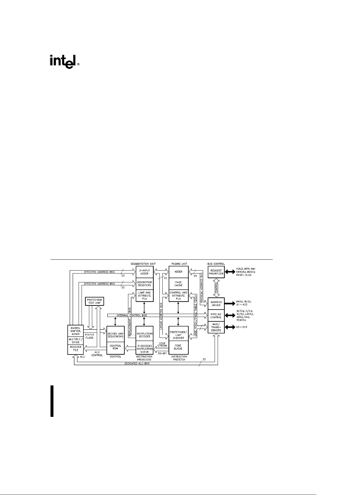
Intel386TMSX Pipelined 32-Bit Microarchitecture

Intel386TMSX MICROPROCESSOR
Intel386TMSX MicroProcessor
CONTENTS PAGE
1.0 PIN DESCRIPTION
АААААААААААААААААААА 3
2.0 BASE ARCHITECTURE АААААААААААААААА 6
2.1 Register Set АААААААААААААААААААААААААААА 6
2.2 Instruction Set ААААААААААААААААААААААААА 10
2.3 Memory Organization АААААААААААААААААА 11
2.4 Addressing Modes АААААААААААААААААААА 12
2.5 Data Types АААААААААААААААААААААААААААА 15
2.6 I/O Space ААААААААААААААААААААААААААААА 15
2.7 Interrupts and Exceptions АААААААААААААА 17
2.8 Reset and Initialization ААААААААААААААААА 20
2.9 Testability ААААААААААААААААААААААААААААА 20
2.10 Debugging Support ААААААААААААААААААА 21
3.0 REAL MODE ARCHITECTURE ААААААА 22
3.1 Memory Addressing ААААААААААААААААААА 22
3.2 Reserved Locations ААААААААААААААААААА 23
3.3 Interrupts АААААААААААААААААААААААААААААА 23
3.4 Shutdown and Halt АААААААААААААААААААА 23
3.5 LOCK Operations ААААААААААААААААААААА 23
4.0 PROTECTED MODE
ARCHITECTURE ААААААААААААААААААААААА 24
4.1 Addressing Mechanism АААААААААААААААА 24
4.2 Segmentation ААААААААААААААААААААААААА 24
4.3 Protection ААААААААААААААААААААААААААААА 29
4.4 Paging АААААААААААААААААААААААААААААААА 33
4.5 Virtual 8086 Environment АААААААААААААА 36
CONTENTS PAGE
5.0 FUNCTIONAL DATA
ААААААААААААААААА 39
5.1 Signal Description Overview ААААААААААА 39
5.2 Bus Transfer Mechanism АААААААААААААА 45
5.3 Memory and I/O Spaces АААААААААААААА 45
5.4 Bus Functional Description АААААААААААА 45
5.5 Self-test Signature ААААААААААААААААААААА 63
5.6 Component and Revision
Identifiers ААААААААААААААААААААААААААААААА 63
5.7 Coprocessor Interfacing ААААААААААААААА 63
6.0 PACKAGE THERMAL
SPECIFICATIONS
АААААААААААААААААААААА 64
7.0 ELECTRICAL SPECIFICATIONS ААААА 64
7.1 Power and Grounding ААААААААААААААААА 64
7.2 Maximum Ratings ААААААААААААААААААААА 65
7.3 D.C. Specifications АААААААААААААААААААА 66
7.4 A.C. Specifications АААААААААААААААААААА 68
7.5 Designing for ICETM-Intel386 SX
Emulator АААААААААААААААААААААААААААААААА 78
8.0 DIFFERENCES BETWEEN THE
Intel386TMSX CPU and the
Intel386TMDX CPU АААААААААААААААААААА 79
9.0 INSTRUCTION SET ААААААААААААААААААА 80
9.1 Intel386TMSX CPU Instruction
Encoding and Clock Count Summary ÀÀÀÀ 80
9.2 Instruction Encoding ААААААААААААААААААА 95
2
Intel386TMSX MICROPROCESSOR
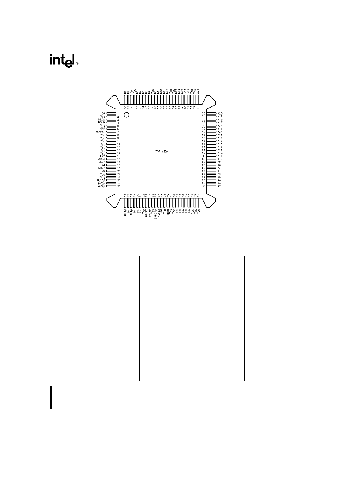
1.0 PIN DESCRIPTION
240187– 1
NOTE:
NC
e
No Connect
Figure 1.1. Intel386TMSX Microprocessor Pin out Top View
Table 1.1. Alphabetical Pin Assignments
Address Data Control N/C V
CC
V
SS
A
1
18 D
0
1 ADS
Ý
16 20 8 2
A
2
51 D
1
100 BHE
Ý
19 27 9 5
A
3
52 D
2
99 BLE
Ý
17 29 10 11
A
4
53 D
3
96 BUSY
Ý
34 30 21 12
A
5
54 D
4
95 CLK2 15 31 32 13
A
6
55 D
5
94 D/C
Ý
24 43 39 14
A
7
56 D
6
93 ERROR
Ý
36 44 42 22
A
8
58 D
7
92 FLT
Ý
28 45 48 35
A
9
59 D
8
90 HLDA 3 46 57 41
A
10
60 D
9
89 HOLD 4 47 69 49
A
11
61 D
10
88 INTR 40 71 50
A
12
62 D
11
87 LOCK
Ý
26 84 63
A
13
64 D
12
86 M/IO
Ý
23 91 67
A
14
65 D
13
83 NA
Ý
69768
A
15
66 D
14
82 NMI 38 77
A
16
70 D
15
81 PEREQ 37 78
A
17
72 READY
Ý
785
A
18
73 RESET 33 98
A
19
74 W/R
Ý
25
A
20
75
A
21
76
A
22
79
A
23
80
3

Intel386TMSX MICROPROCESSOR
1.0 PIN DESCRIPTION (Continued)
The following are the Intel386TMSX Microprocessor pin descriptions. The following definitions are used in the
pin descriptions:
Ý
The named signal is active LOW.
I Input signal.
O Output signal.
I/O Input and Output signal.
- No electrical connection.
Symbol Type Pin Name and Function
CLK2 I 15 CLK2 provides the fundamental timing for the Intel386 SX
Microprocessor. For additional information see Clock.
RESET I 33 RESET suspends any operation in progress and places the
Intel386 SX Microprocessor in a known reset state. See
Interrupt Signals for additional information.
D15–D
0
I/O 81-83,86-90, Data Bus inputs data during memory, I/O and interrupt
acknowledge read cycles and outputs data during memory and
92-96,99-100,1
I/O write cycles. See Data Bus for additional information.
A23–A
1
O 80-79,76-72,70, Address Bus outputs physical memory or port I/O addresses.
See Address Bus for additional information.
66-64,62-58,
56-51,18
W/R
Ý
O25 Write/Read is a bus cycle definition pin that distinguishes write
cycles from read cycles. See Bus Cycle Definition Signals for
additional information.
D/C
Ý
O24 Data/Control is a bus cycle definition pin that distinguishes data
cycles, either memory or I/O, from control cycles which are:
interrupt acknowledge, halt, and code fetch. See Bus Cycle
Definition Signals for additional information.
M/IO
Ý
O23 Memory/IO is a bus cycle definition pin that distinguishes
memory cycles from input/output cycles. See Bus Cycle
Definition Signals for additional information.
LOCK
Ý
O26 Bus Lock is a bus cycle definition pin that indicates that other
system bus masters are not to gain control of the system bus
while it is active. See Bus Cycle Definition Signals for
additional information.
ADS
Ý
O16 Address Status indicates that a valid bus cycle definition and
address (W/R
Ý
, D/CÝ, M/IOÝ, BHEÝ, BLEÝand A23–A1are
being driven at the Intel386 SX Microprocessor pins. See Bus
Control Signals for additional information.
NA
Ý
I6 Next Address is used to request address pipelining. See Bus
Control Signals for additional information.
READY
Ý
I7 Bus Ready terminates the bus cycle. See Bus Control Signals
for additional information.
BHEÝ, BLE
Ý
O 19,17 Byte Enables indicate which data bytes of the data bus take part
in a bus cycle. See Address Bus for additional information.
4

Intel386TMSX MICROPROCESSOR
1.0 PIN DESCRIPTION (Continued)
Symbol Type Pin Name and Function
HOLD I 4 Bus Hold Request input allows another bus master to request
control of the local bus. See Bus Arbitration Signals for
additional information.
HLDA O 3 Bus Hold Acknowledge output indicates that the Intel386 SX
Microprocessor has surrendered control of its local bus to
another bus master. See Bus Arbitration Signals for additional
information.
INTR I 40 Interrupt Request is a maskable input that signals the Intel386
SX Microprocessor to suspend execution of the current program
and execute an interrupt acknowledge function. See Interrupt
Signals for additional information.
NMI I 38 Non-Maskable Interrupt Request is a non-maskable input that
signals the Intel386 SX Microprocessor to suspend execution of
the current program and execute an interrupt acknowledge
function. See Interrupt Signals for additional information.
BUSY
Ý
I34 Busy signals a busy condition from a processor extension. See
Coprocessor Interface Signals for additional information.
ERROR
Ý
I36 Error signals an error condition from a processor extension. See
Coprocessor Interface Signals for additional information.
PEREQ I 37 Processor Extension Request indicates that the processor has
data to be transferred by the Intel386 SX Microprocessor. See
Coprocessor Interface Signals for additional information.
FLT
Ý
I28 Float is an input which forces all bidirectional and output signals,
including HLDA, to the tri-state condition. This allows the
electrically isolated Intel386SX PQFP to use ONCE (On-Circuit
Emulation) method without removing it from the PCB. See Float
for additional information.
N/C - 20, 27, 29-31, 43-47 No Connects should always be left unconnected. Connection of
a N/C pin may cause the processor to malfunction or be
incompatible with future steppings of the Intel386 SX
Microprocessor.
V
CC
I 8-10,21,32,39 System Power provides thea5V nominal DC supply input.
42,48,57,69,
71,84,91,97
V
SS
I 2,5,11-14,22 System Ground provides the 0V connection from which all
inputs and outputs are measured.
35,41,49-50,
63,67-68,
77-78,85,98
5

Intel386TMSX MICROPROCESSOR
INTRODUCTION
The Intel386 SX Microprocessor is 100% object
code compatible with the Intel386 DX, 286 and 8086
microprocessors. Systems based on the Intel386 SX
CPU can access the world’s largest existing microcomputer software base, including the growing 32bit software base.
Instruction pipelining and a high performance ALU
ensure short average instruction execution times
and high system throughput.
The integrated memory management unit (MMU) includes an address translation cache, multi-tasking
hardware, and a four-level hardware-enforced protection mechanism to support operating systems.
The virtual machine capability of the Intel386 SX
CPU allows simultaneous execution of applications
from multiple operating systems.
The Intel386 SX CPU offers on-chip testability and
debugging features. Four breakpoint registers allow
conditional or unconditional breakpoint traps on
code execution or data accesses for powerful debugging of even ROM-based systems. Other testability features include self-test, tri-state of output
buffers, and direct access to the page translation
cache.
The Low Power Intel386 SX CPU brings the benefits
of the Intel386 Microprocessor 32-bit architecture to
Laptop and Notebook personal computer applications. With its power saving 2 MHz sleep-mode and
extended functional temperature range of 0
§
Cto
100
§
CT
CASE
, the Lower Power Intel386 SX CPU
specifically satisfies the power consumption and
heat dissipation requirements of today’s small form
factor computers.
2.0 BASE ARCHITECTURE
The Intel386 SX Microprocessor consists of a central processing unit, a memory management unit and
a bus interface.
The central processing unit consists of the execution unit and the instruction unit. The execution unit
contains the eight 32-bit general purpose registers
which are used for both address calculation and
data operations and a 64-bit barrel shifter used to
speed shift, rotate, multiply, and divide operations.
The instruction unit decodes the instruction opcodes
and stores them in the decoded instruction queue
for immediate use by the execution unit.
The memory management unit (MMU) consists of a
segmentation unit and a paging unit. Segmentation
allows the managing of the logical address space by
providing an extra addressing component, one that
allows easy code and data relocatability, and efficient sharing. The paging mechanism operates beneath and is transparent to the segmentation process, to allow management of the physical address
space.
The segmentation unit provides four levels of protection for isolating and protecting applications and
the operating system from each other. The hardware
enforced protection allows the design of systems
with a high degree of integrity.
The Intel386 SX Microprocessor has two modes of
operation: Real Address Mode (Real Mode), and
Protected Virtual Address Mode (Protected Mode).
In Real Mode the Intel386 SX Microprocessor operates as a very fast 8086, but with 32-bit extensions if
desired. Real Mode is required primarily to set up the
processor for Protected Mode operation.
Within Protected Mode, software can perform a task
switch to enter into tasks designated as Virtual 8086
Mode tasks. Each such task behaves with 8086 semantics, thus allowing 8086 software (an application
program or an entire operating system) to execute.
The Virtual 8086 tasks can be isolated and protected from one another and the host Intel386 SX Microprocessor operating system by use of paging.
Finally, to facilitate system hardware designs, the
Intel386 SX Microprocessor bus interface offers address pipelining and direct Byte Enable signals for
each byte of the data bus.
2.1 Register Set
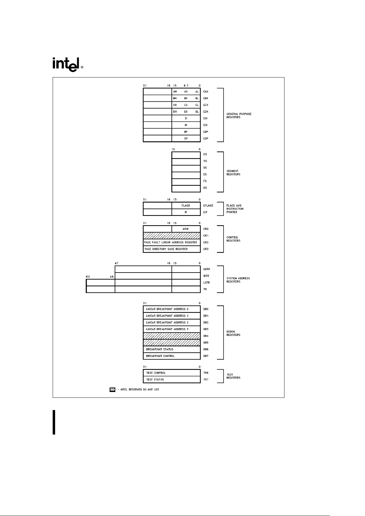
The Intel386 SX Microprocessor has thirty-four registers as shown in Figure 2-1. These registers are
grouped into the following seven categories:
General Purpose Registers: The eight 32-bit general purpose registers are used to contain arithmetic
and logical operands. Four of these (EAX, EBX,
ECX, and EDX) can be used either in their entirety as
32-bit registers, as 16-bit registers, or split into pairs
of separate 8-bit registers.
6
Intel386TMSX MICROPROCESSOR
240187– 2
Figure 2.1. Intel386TMSX Microprocessor Registers
7
Intel386TMSX MICROPROCESSOR
Segment Registers: Six 16-bit special purpose reg-
isters select, at any given time, the segments of
memory that are immediately addressable for code,
stack, and data.
Flags and Instruction Pointer Registers: The two
32-bit special purpose registers in figure 2.1 record
or control certain aspects of the Intel386 SX Microprocessor state. The EFLAGS register includes
status and control bits that are used to reflect the
outcome of many instructions and modify the semantics of some instructions. The Instruction Pointer, called EIP, is 32 bits wide. The Instruction Pointer
controls instruction fetching and the processor automatically increments it after executing an instruction.
Control Registers: The four 32-bit control register
are used to control the global nature of the Intel386
SX Microprocessor. The CR0 register contains bits
that set the different processor modes (Protected,
Real, Paging and Coprocessor Emulation). CR2 and
CR3 registers are used in the paging operation.
System Address Registers: These four special
registers reference the tables or segments supported by the 80286/Intel386 SX/Intel386 DX CPU’s
protection model. These tables or segments are:
GDTR (Global Descriptor Table Register),
IDTR (Interrupt Descriptor Table Register),
LDTR (Local Descriptor Table Register),
TR (Task State Segment Register).
Debug Registers: The six programmer accessible
debug registers provide on-chip support for debugging. The use of the debug registers is described in
Section 2.10 Debugging Support.
Test Registers: Two registers are used to control
the testing of the RAM/CAM (Content Addressable
Memories) in the Translation Lookaside Buffer portion of the Intel386 SX Microprocessor. Their use is
discussed in Testability.
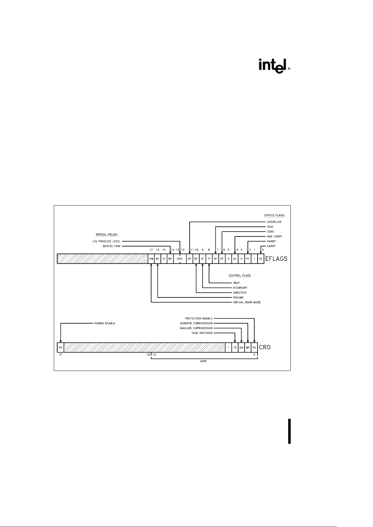
240187– 3
Figure 2.2. Status and Control Register Bit Functions
8

Intel386TMSX MICROPROCESSOR
EFLAGS REGISTER
The flag register is a 32-bit register named EFLAGS.
The defined bits and bit fields within EFLAGS,
shown in Figure 2.2, control certain operations and
indicate the status of the Intel386 SX Microprocessor. The lower 16 bits (bits 0–15) of EFLAGS contain the 16-bit flag register named FLAGS. This is
the default flag register used when executing 8086,
80286, or real mode code. The functions of the flag
bits are given in Table 2.1.
CONTROL REGISTERS
The Intel386 SX Microprocessor has three control
registers of 32 bits, CR0, CR2 and CR3, to hold the
machine state of a global nature. These registers
are shown in Figures 2.1 and 2.2. The defined CR0
bits are described in Table 2.2.
Table 2.1. Flag Definitions
Bit Position Name Function
0 CF Carry FlagÐSet on high-order bit carry or borrow; cleared
otherwise.
2 PF Parity FlagÐSet if low-order 8 bits of result contain an even
number of 1-bits; cleared otherwise.
4 AF Auxiliary Carry FlagÐSet on carry from or borrow to the low
order four bits of AL; cleared otherwise.
6 ZF Zero FlagÐSet if result is zero; cleared otherwise.
7 SF Sign FlagÐSet equal to high-order bit of result (0 if positive, 1 if
negative).
8 TF Single Step FlagÐOnce set, a single step interrupt occurs after
the next instruction executes. TF is cleared by the single step
interrupt.
9 IF Interrupt-Enable FlagÐWhen set, maskable interrupts will cause
the CPU to transfer control to an interrupt vector specified
location.
10 DF Direction FlagÐCauses string instructions to auto-increment
(default) the appropriate index registers when cleared. Setting
DF causes auto-decrement.
11 OF Overflow FlagÐSet if the operation resulted in a carry/borrow
into the sign bit (high-order bit) of the result but did not result in a
carry/borrow out of the high-order bit or vice-versa.
12,13 IOPL I/O Privilege LevelÐIndicates the maximum Current Privilege
Level (CPL) permitted to execute I/O instructions without
generating an exception 13 fault or consulting the I/O permission
bit map while executing in protected mode. For virtual 86 mode it
indicates the maximum CPL allowing alteration of the IF bit. See
Section 4.2 for a further discussion and definitions on various
privilege levels.
14 NT Nested TaskÐSet if the execution of the current task is nested
within another task. Cleared otherwise.
16 RF Resume FlagÐUsed in conjunction with debug register
breakpoints. It is checked at instruction boundaries before
breakpoint processing. If set, any debug fault is ignored on the
next instruction.
17 VM Virtual 8086 ModeÐIf set while in protected mode, the Intel386
SX Microprocessor will switch to virtual 8086 operation, handling
segment loads as the 8086 does, but generating exception 13
faults on privileged opcodes.
9

Intel386TMSX MICROPROCESSOR
Table 2.2. CR0 Definitions
Bit Position Name Function
0 PE Protection mode enableÐplaces the Intel386 SX Microprocessor
into protected mode. If PE is reset, the processor operates again
in Real Mode. PE may be set by loading MSW or CR0. PE can be
reset only by loading CR0, it cannot be reset by the LMSW
instruction.
1 MP Monitor coprocessor extensionÐallows WAIT instructions to
cause a processor extension not present exception (number 7).
2 EM Emulate processor extensionÐcauses a processor extension
not present exception (number 7) on ESC instructions to allow
emulating a processor extension.
3 TS Task switchedÐindicates the next instruction using a processor
extension will cause exception 7, allowing software to test
whether the current processor extension context belongs to the
current task.
31 PG Paging enable bitÐis set to enable the on-chip paging unit. It is
reset to disable the on-chip paging unit.
2.2 Instruction Set
The instruction set is divided into nine categories of
operations:
Data Transfer
Arithmetic
Shift/Rotate
String Manipulation
Bit Manipulation
Control Transfer
High Level Language Support
Operating System Support
Processor Control
These instructions are listed in Table 9.1 Instruc-
tion Set Clock Count Summary.
All Intel386 SX Microprocessor instructions operate
on either 0, 1, 2 or 3 operands; an operand resides
in a register, in the instruction itself, or in memory.
Most zero operand instructions (e.g CLI, STI) take
only one byte. One operand instructions generally
are two bytes long. The average instruction is 3.2
bytes long. Since the Intel386 SX Microprocessor
has a 16 byte prefetch instruction queue, an average
of 5 instructions will be prefetched. The use of two
operands permits the following types of common instructions:
Register to Register
Memory to Register
Immediate to Register
Memory to Memory
Register to Memory
Immediate to Memory.
The operands can be either 8, 16, or 32 bits long. As
a general rule, when executing code written for the
Intel386 SX Microprocessor (32-bit code), operands
are 8 or 32 bits; when executing existing 8086 or
80286 code (16-bit code), operands are 8 or 16 bits.
Prefixes can be added to all instructions which override the default length of the operands (i.e. use
32-bit operands for 16-bit code, or 16-bit operands
for 32-bit code).
10

Intel386TMSX MICROPROCESSOR
2.3 Memory Organization
Memory on the Intel386 SX Microprocessor is divided into 8-bit quantities (bytes), 16-bit quantities
(words), and 32-bit quantities (dwords). Words are
stored in two consecutive bytes in memory with the
low-order byte at the lowest address. Dwords are
stored in four consecutive bytes in memory with the
low-order byte at the lowest address. The address of
a word or dword is the byte address of the low-order
byte.
In addition to these basic data types, the Intel386 SX
Microprocessor supports two larger units of memory:
pages and segments. Memory can be divided up
into one or more variable length segments, which
can be swapped to disk or shared between programs. Memory can also be organized into one or
more 4K byte pages. Finally, both segmentation and
paging can be combined, gaining the advantages of
both systems. The Intel386 SX Microprocessor supports both pages and segmentation in order to provide maximum flexibility to the system designer.
Segmentation and paging are complementary. Segmentation is useful for organizing memory in logical
modules, and as such is a tool for the application
programmer, while pages are useful to the system
programmer for managing the physical memory of a
system.
ADDRESS SPACES
The Intel386 SX Microprocessor has three types of
address spaces: logical, linear, and physical.A
logical address (also known as a virtual address)
consists of a selector and an offset. A selector is the
contents of a segment register. An offset is formed
by summing all of the addressing components
(BASE, INDEX, DISPLACEMENT), discussed in section 2.4 Addressing Modes, into an effective address. This effective address along with the selector
is known as the logical address. Since each task on
the Intel386 SX Microprocessor has a maximum of
16K (2
14
b
1) selectors, and offsets can be 4 giga-
bytes (with paging enabled) this gives a total of 2
46
bits, or 64 terabytes, of logical address space per
task. The programmer sees the logical address
space.
The segmentation unit translates the logical address space into a 32-bit linear address space. If the
paging unit is not enabled then the 32-bit linear address is truncated into a 24-bit physical address.
The physical address is what appears on the address pins.
The primary differences between Real Mode and
Protected Mode are how the segmentation unit performs the translation of the logical address into the
linear address, size of the address space, and paging capability. In Real Mode, the segmentation unit
shifts the selector left four bits and adds the result to
the effective address to form the linear address.
This linear address is limited to 1 megabyte. In addition, real mode has no paging capability.
Protected Mode will see one of two different address spaces, depending on whether or not paging
is enabled. Every selector has a logical base address associated with it that can be up to 32 bits in
length. This 32-bit logical base address is added to
the effective address to form a final 32-bit linear
address. If paging is disabled this final linear address reflects physical memory and is truncated so
that only the lower 24 bits of this address are used
to address the 16 megabyte memory address space.
If paging is enabled this final linear address reflects
a 32-bit address that is translated through the paging unit to form a 16-megabyte physical address.
The logical base address is stored in one of two
operating system tables (i.e. the Local Descriptor
Table or Global Descriptor Table).
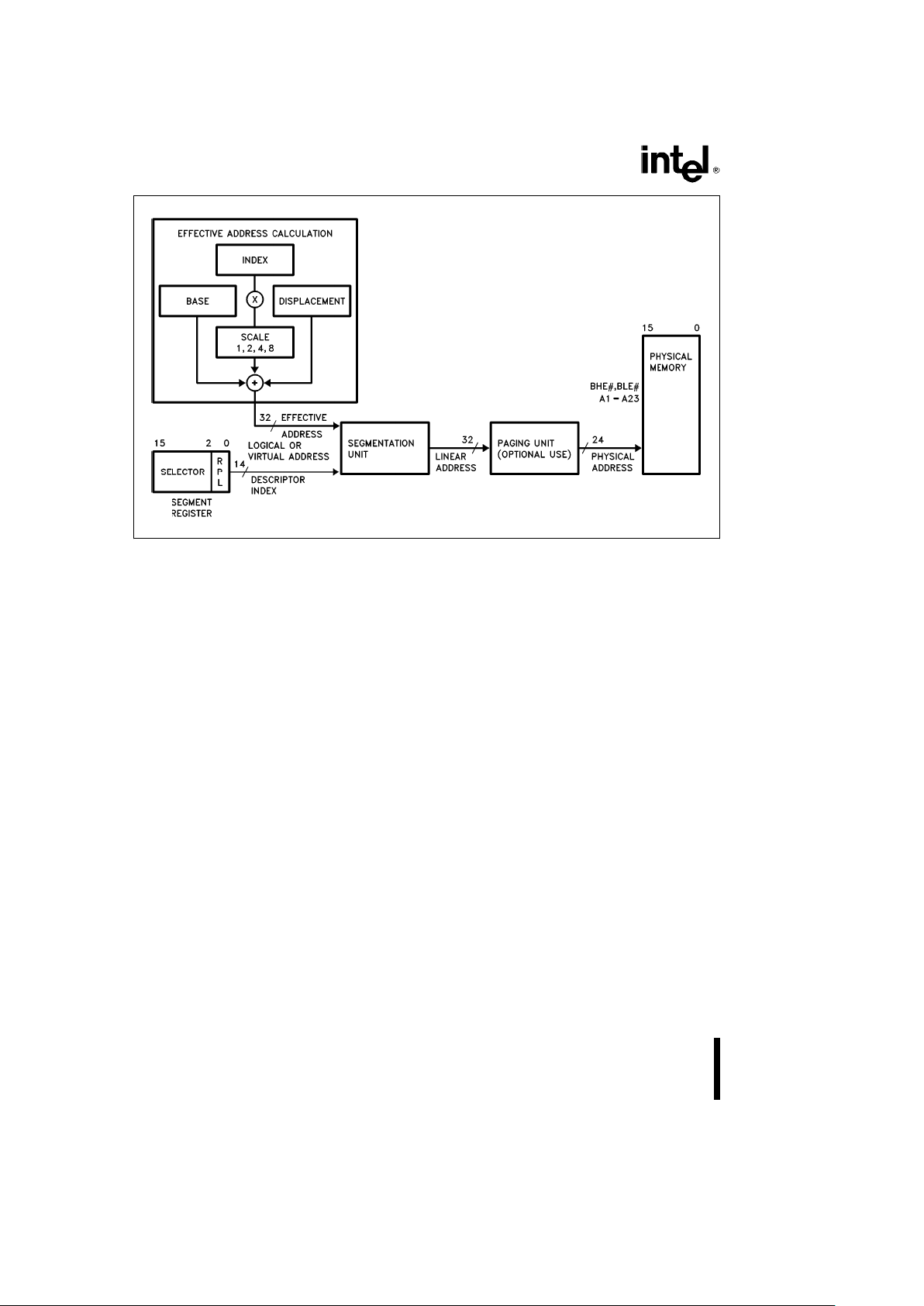
Figure 2.3 shows the relationship between the various address spaces.
11
Intel386TMSX MICROPROCESSOR
240187– 4
Figure 2.3. Address Translation
SEGMENT REGISTER USAGE
The main data structure used to organize memory is
the segment. On the Intel386 SX Microprocessor,
segments are variable sized blocks of linear addresses which have certain attributes associated
with them. There are two main types of segments,
code and data. The segments are of variable size
and can be as small as 1 byte or as large as 4 gigabytes (2
32
bits).
In order to provide compact instruction encoding
and increase processor performance, instructions
do not need to explicitly specify which segment register is used. The segment register is automatically
chosen according to the rules of Table 2.3 (Segment
Register Selection Rules). In general, data references use the selector contained in the DS register,
stack references use the SS register and instruction
fetches use the CS register. The contents of the Instruction Pointer provide the offset. Special segment
override prefixes allow the explicit use of a given
segment register, and override the implicit rules listed in Table 2.3. The override prefixes also allow the
use of the ES, FS and GS segment registers.
There are no restrictions regarding the overlapping
of the base addresses of any segments. Thus, all 6
segments could have the base address set to zero
and create a system with a four gigabyte linear ad-
dress space. This creates a system where the virtual
address space is the same as the linear address
space. Further details of segmentation are discussed in chapter 4 PROTECTED MODE ARCHI-
TECTURE.
2.4 Addressing Modes
The Intel386 SX Microprocessor provides a total of 8
addressing modes for instructions to specify operands. The addressing modes are optimized to allow
the efficient execution of high level languages such
as C and FORTRAN, and they cover the vast majority of data references needed by high-level languages.
REGISTER AND IMMEDIATE MODES
Two of the addressing modes provide for instructions that operate on register or immediate operands:
Register Operand Mode: The operand is located in
one of the 8, 16 or 32-bit general registers.
Immediate Operand Mode: The operand is included in the instruction as part of the opcode.
12

Intel386TMSX MICROPROCESSOR
Table 2.3. Segment Register Selection Rules
Type of Implied (Default) Segment Override
Memory Reference Segment Use Prefixes Possible
Code Fetch CS None
Destination of PUSH, PUSHF, INT,
CALL, PUSHA Instructons SS None
Source of POP, POPA, POPF, IRET,
RET Instructions SS None
Destination of STOS, MOVE, REP STOS,
and REP MOVS instructions ES None
Other data references, with effective
address using base register of:
[
EAX
]
DS CS,SS,ES,FS,GS
[
EBX
]
DS CS,SS,ES,FS,GS
[
ECX
]
DS CS,SS,ES,FS,GS
[
EDX
]
DS CS,SS,ES,FS,GS
[
ESI
]
DS CS,SS,ES,FS,GS
[
EDI
]
DS CS,SS,ES,FS,GS
[
EBP
]
SS CS,DS,ES,FS,GS
[
ESP
]
SS CS,DS,ES,FS,GS
32-BIT MEMORY ADDRESSING MODES
The remaining 6 modes provide a mechanism for
specifying the effective address of an operand. The
linear address consists of two components: the segment base address and an effective address. The
effective address is calculated by summing any
combination of the following three address elements
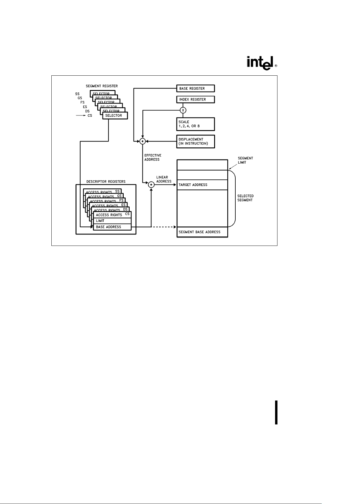
(see Figure 2.3):
DISPLACEMENT: an 8, 16 or 32-bit immediate value, following the instruction.
BASE: The contents of any general purpose register. The base registers are generally used by compilers to point to the start of the local variable area.
INDEX: The contents of any general purpose register except for ESP. The index registers are used to
access the elements of an array, or a string of characters. The index register’s value can be multiplied
by a scale factor, either 1, 2, 4 or 8. The scaled index
is especially useful for accessing arrays or structures.
Combinations of these 3 components make up the 6
additional addressing modes. There is no performance penalty for using any of these addressing combinations, since the effective address calculation is
pipelined with the execution of other instructions.
The one exception is the simultaneous use of Base
and Index components which requires one additional clock.
As shown in Figure 2.4, the effective address (EA) of
an operand is calculated according to the following
formula:
EAeBase
Register
a
(Index
Register
*scaling)
a
Displacement
1. Direct Mode: The operand’s offset is contained
as part of the instruction as an 8, 16 or 32-bit
displacement.
2. Register Indirect Mode: A BASE register contains the address of the operand.
3. Based Mode: A BASE register’s contents are
added to a DISPLACEMENT to form the operand’s offset.
4. Scaled Index Mode: An INDEX register’s contents are multiplied by a SCALING factor, and the
result is added to a DISPLACEMENT to form the
operand’s offset.
5. Based Scaled Index Mode: The contents of an
INDEX register are multiplied by a SCALING factor, and the result is added to the contents of a
BASE register to obtain the operand’s offset.
6. Based Scaled Index Mode with Displacement:
The contents of an INDEX register are multiplied
by a SCALING factor, and the result is added to
the contents of a BASE register and a DISPLACEMENT to form the operand’s offset.
13
Intel386TMSX MICROPROCESSOR
240187– 5
Figure 2.4. Addressing Mode Calculations
DIFFERENCES BETWEEN 16 AND 32 BIT
ADDRESSES
In order to provide software compatibility with the
8086 and the 80286, the Intel386 SX Microprocessor can execute 16-bit instructions in Real and Protected Modes. The processor determines the size of
the instructions it is executing by examining the D bit
in a Segment Descriptor. If the D bit is 0 then all
operand lengths and effective addresses are assumed to be 16 bits long. If the D bit is 1 then the
default length for operands and addresses is 32 bits.
In Real Mode the default size for operands and addresses is 16 bits.
Regardless of the default precision of the operands
or addresses, the Intel386 SX Microprocessor is
able to execute either 16 or 32-bit instructions. This
is specified through the use of override prefixes.
Two prefixes, the Operand Length Prefix and the
Address Length Prefix, override the value of the D
bit on an individual instruction basis. These prefixes
are automatically added by assemblers.
The Operand Length and Address Length Prefixes
can be applied separately or in combination to any
instruction. The Address Length Prefix does not allow addresses over 64K bytes to be accessed in
Real Mode. A memory address which exceeds
0FFFFH will result in a General Protection Fault. An
Address Length Prefix only allows the use of the additional Intel386 SX Microprocessor addressing
modes.
When executing 32-bit code, the Intel386 SX Microprocessor uses either 8 or 32-bit displacements, and
any register can be used as base or index registers.
When executing 16-bit code, the displacements are
either 8 or 16-bits, and the base and index register
conform to the 80286 model. Table 2.4 illustrates
the differences.
14

Intel386TMSX MICROPROCESSOR
Table 2.4. BASE and INDEX Registers for 16- and 32-Bit Addresses
16-Bit Addressing 32-Bit Addressing
BASE REGISTER BX,BP Any 32-bit GP Register
INDEX REGISTER SI,DI Any 32-bit GP Register
Except ESP
SCALE FACTOR None 1, 2, 4, 8
DISPLACEMENT 0, 8, 16-bits 0, 8, 32-bits
2.5 Data Types
The Intel386 SX Microprocessor supports all of the
data types commonly used in high level languages:
Bit: A single bit quantity.
Bit Field: A group of up to 32 contiguous bits, which
spans a maximum of four bytes.
Bit String: A set of contiguous bits; on the Intel386
SX Microprocessor, bit strings can be up to 4 gigabits long.
Byte: A signed 8-bit quantity.
Unsigned Byte: An unsigned 8-bit quantity.
Integer (Word): A signed 16-bit quantity.
Long Integer (Double Word): A signed 32-bit quan-
tity. All operations assume a 2’s complement representation.
Unsigned Integer (Word): An unsigned 16-bit
quantity.
Unsigned Long Integer (Double Word): An unsigned 32-bit quantity.
Signed Quad Word: A signed 64-bit quantity.
Unsigned Quad Word: An unsigned 64-bit quantity.
Pointer: A 16 or 32-bit offset-only quantity which in-
directly references another memory location.
Long Pointer: A full pointer which consists of a 16bit segment selector and either a 16 or 32-bit offset.
Char: A byte representation of an ASCII Alphanumeric or control character.
String: A contiguous sequence of bytes, words or
dwords. A string may contain between 1 byte and 4
gigabytes.
BCD: A byte (unpacked) representation of decimal
digits 0–9.
Packed BCD: A byte (packed) representation of two
decimal digits 0– 9 storing one digit in each nibble.
When the Intel386 SX Microprocessor is coupled
with its numerics coprocessor, the Intel387 SX, then
the following common floating point types are supported:
Floating Point: A signed 32, 64, or 80-bit real number representation. Floating point numbers are supported by the Intel387 SX numerics coprocessor.
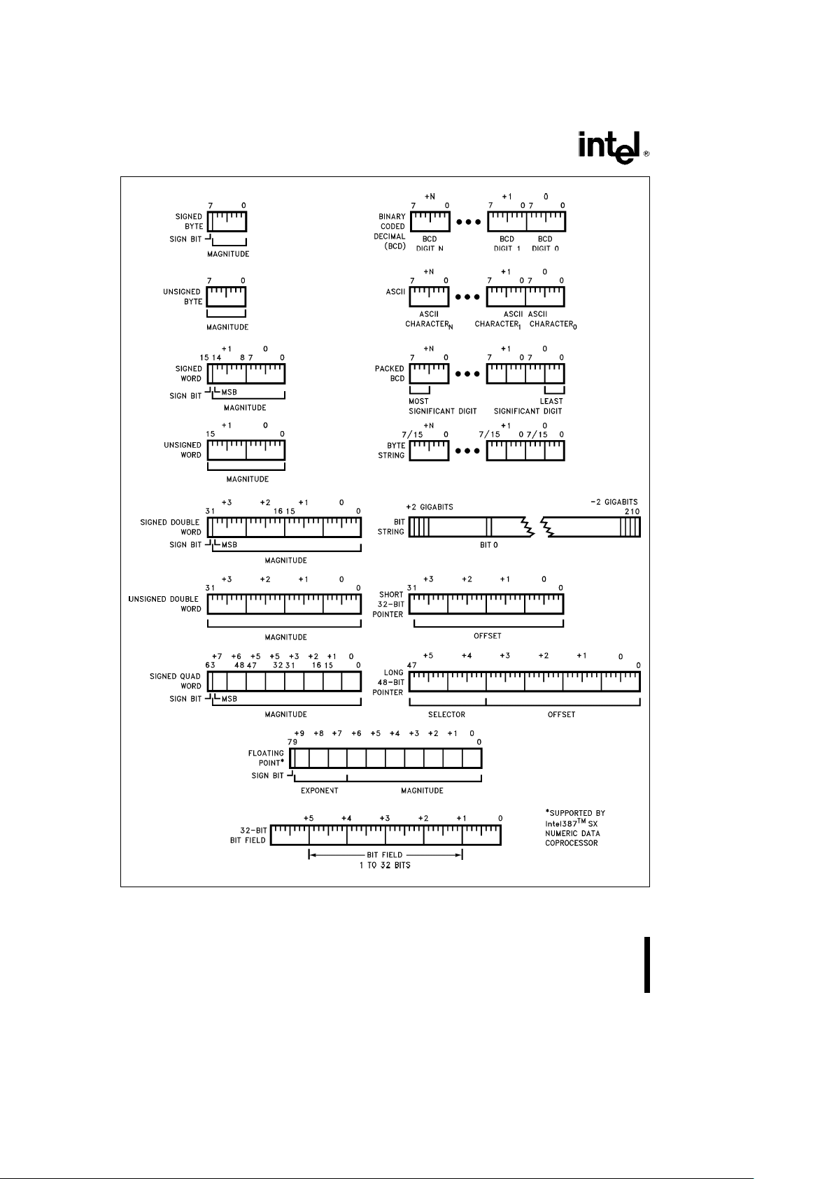
Figure 2.5 illustrates the data types supported by the
Intel386 SX Microprocessor and the Intel387 SX.
2.6 I/O Space
The Intel386 SX Microprocessor has two distinct
physical address spaces: physical memory and I/O.
Generally, peripherals are placed in I/O space although the Intel386 SX Microprocessor also supports memory-mapped peripherals. The I/O space
consists of 64K bytes which can be divided into 64K
8-bit ports or 32K 16-bit ports, or any combination of
ports which add up to no more than 64K bytes. The
64K I/O address space refers to physical addresses
rather than linear addresses since I/O instructions
do not go through the segmentation or paging hardware. The M/IO
Ý
pin acts as an additional address
line, thus allowing the system designer to easily determine which address space the processor is accessing.
The I/O ports are accessed by the IN and OUT instructions, with the port address supplied as an immediate 8-bit constant in the instruction or in the DX
register. All 8-bit and 16-bit port addresses are zero
extended on the upper address lines. The I/O instructions cause the M/IO
Ý
pin to be driven LOW.
I/O port addresses 00F8H through 00FFH are reserved for use by Intel.
15
Intel386TMSX MICROPROCESSOR
240187– 6
Figure 2.5. Intel386TMSX Microprocessor Supported Data Types
16

Intel386TMSX MICROPROCESSOR
2.7 Interrupts and Exceptions
Interrupts and exceptions alter the normal program
flow in order to handle external events, report errors
or exceptional conditions. The difference between
interrupts and exceptions is that interrupts are used
to handle asynchronous external events while exceptions handle instruction faults. Although a program can generate a software interrupt via an INT N
instruction, the processor treats software interrupts
as exceptions.
Hardware interrupts occur as the result of an external event and are classified into two types: maskable
or non-maskable. Interrupts are serviced after the
execution of the current instruction. After the interrupt handler is finished servicing the interrupt, execution proceeds with the instruction immediately
after the interrupted instruction.
Exceptions are classified as faults, traps, or aborts,
depending on the way they are reported and whether or not restart of the instruction causing the exception is supported. Faults are exceptions that are detected and serviced before the execution of the
faulting instruction. Traps are exceptions that are
reported immediately after the execution of the instruction which caused the problem. Aborts are exceptions which do not permit the precise location of
the instruction causing the exception to be determined.
Thus, when an interrupt service routine has been
completed, execution proceeds from the instruction
immediately following the interrupted instruction. On
the other hand, the return address from an exception fault routine will always point to the instruction
causing the exception and will include any leading
instruction prefixes. Table 2.5 summarizes the possible interrupts for the Intel386 SX Microprocessor
and shows where the return address points to.
Table 2.5. Interrupt Vector Assignments
Return Address
Interrupt
Instruction Which
Points to
Function
Number
Can Cause
Faulting
Type
Exception
Instruction
Divide Error 0 DIV, IDIV YES FAULT
Debug Exception 1 any instruction YES TRAP*
NMI Interrupt 2 INT 2 or NMI NO NMI
One Byte Interrupt 3 INT NO TRAP
Interrupt on Overflow 4 INTO NO TRAP
Array Bounds Check 5 BOUND YES FAULT
Invalid OP-Code 6 Any illegal instruction YES FAULT
Device Not Available 7 ESC, WAIT YES FAULT
Double Fault 8
Any instruction that can
ABORT
generate an exception
Coprocessor Segment Overrun 9 ESC NO ABORT
Invalid TSS 10 JMP, CALL, IRET, INT YES FAULT
Segment Not Present 11 Segment Register Instructions YES FAULT
Stack Fault 12 Stack References YES FAULT
General Protection Fault 13 Any Memory Reference YES FAULT
Page Fault 14 Any Memory Access or Code Fetch YES FAULT
Coprocessor Error 16 ESC, WAIT YES FAULT
Intel Reserved 17–32
Two Byte Interrupt 33– 255 INT n NO TRAP
*Some debug exceptions may report both traps on the previous instruction and faults on the next instruction.
17

Intel386TMSX MICROPROCESSOR
The Intel386 SX Microprocessor has the ability to
handle up to 256 different interrupts/exceptions. In
order to service the interrupts, a table with up to 256
interrupt vectors must be defined. The interrupt vectors are simply pointers to the appropriate interrupt
service routine. In Real Mode, the vectors are 4-byte
quantities, a Code Segment plus a 16-bit offset; in
Protected Mode, the interrupt vectors are 8 byte
quantities, which are put in an Interrupt Descriptor
Table. Of the 256 possible interrupts, 32 are reserved for use by Intel and the remaining 224 are
free to be used by the system designer.
INTERRUPT PROCESSING
When an interrupt occurs, the following actions happen. First, the current program address and Flags
are saved on the stack to allow resumption of the
interrupted program. Next, an 8-bit vector is supplied
to the Intel386 SX Microprocessor which identifies
the appropriate entry in the interrupt table. The table
contains the starting address of the interrupt service
routine. Then, the user supplied interrupt service
routine is executed. Finally, when an IRET instruction is executed the old processor state is restored
and program execution resumes at the appropriate
instruction.
The 8-bit interrupt vector is supplied to the Intel386
SX Microprocessor in several different ways: exceptions supply the interrupt vector internally; software
INT instructions contain or imply the vector; maskable hardware interrupts supply the 8-bit vector via
the interrupt acknowledge bus sequence. NonMaskable hardware interrupts are assigned to interrupt vector 2.
Maskable Interrupt
Maskable interrupts are the most common way to
respond to asynchronous external hardware events.
A hardware interrupt occurs when the INTR is pulled
HIGH and the Interrupt Flag bit (IF) is enabled. The
processor only responds to interrupts between instructions (string instructions have an ‘interrupt window‘ between memory moves which allows interrupts during long string moves). When an interrupt
occurs the processor reads an 8-bit vector supplied
by the hardware which identifies the source of the
interrupt (one of 224 user defined interrupts).
Interrupts through interrupt gates automatically reset
IF, disabling INTR requests. Interrupts through Trap
Gates leave the state of the IF bit unchanged. Interrupts through a Task Gate change the IF bit according to the image of the EFLAGs register in the task’s
Task State Segment (TSS). When an IRET instruction is executed, the original state of the IF bit is
restored.
Non-Maskable Interrupt
Non-maskable interrupts provide a method of servicing very high priority interrupts. When the NMI input
is pulled HIGH it causes an interrupt with an internally supplied vector value of 2. Unlike a normal hardware interrupt, no interrupt acknowledgment sequence is performed for an NMI.
While executing the NMI servicing procedure, the Intel386 SX Microprocessor will not service any further
NMI request or INT requests until an interrupt return
(IRET) instruction is executed or the processor is
reset. If NMI occurs while currently servicing an NMI,
its presence will be saved for servicing after executing the first IRET instruction. The IF bit is cleared at
the beginning of an NMI interrupt to inhibit further
INTR interrupts.
Software Interrupts
A third type of interrupt/exception for the Intel386
SX Microprocessor is the software interrupt. An INT
n instruction causes the processor to execute the
interrupt service routine pointed to by the n
th
vector
in the interrupt table.
A special case of the two byte software interrupt INT
n is the one byte INT 3, or breakpoint interrupt. By
inserting this one byte instruction in a program, the
user can set breakpoints in his program as a debugging tool.
A final type of software interrupt is the single step
interrupt. It is discussed in Single Step Trap.
18

Intel386TMSX MICROPROCESSOR
INTERRUPT AND EXCEPTION PRIORITIES
Interrupts are externally generated events. Maskable Interrupts (on the INTR input) and Non-Maskable
Interrupts (on the NMI input) are recognized at instruction boundaries. When NMI and maskable
INTR are both recognized at the same instruction
boundary, the Intel386 SX Microprocessor invokes
the NMI service routine first. If maskable interrupts
are still enabled after the NMI service routine has
been invoked, then the Intel386 SX Microprocessor
will invoke the appropriate interrupt service routine.
As the Intel386 SX Microprocessor executes instructions, it follows a consistent cycle in checking for
exceptions, as shown in Table 2.6. This cycle is re-
peated as each instruction is executed, and occurs
in parallel with instruction decoding and execution.
INSTRUCTION RESTART
The Intel386 SX Microprocessor fully supports restarting all instructions after Faults. If an exception is
detected in the instruction to be executed (exception
categories 4 through 10 in Table 2.6), the Intel386
SX Microprocessor invokes the appropriate exception service routine. The Intel386 SX Microprocessor
is in a state that permits restart of the instruction, for
all cases but those given in Table 2.7. Note that all
such cases will be avoided by a properly designed
operating system.
Table 2.6. Sequence of Exception Checking
Consider the case of the Intel386 SX Microprocessor having just completed an instruction. It then performs
the following checks before reaching the point where the next instruction is completed:
1. Check for Exception 1 Traps from the instruction just completed (single-step via Trap Flag, or Data
Breakpoints set in the Debug Registers).
2. Check for external NMI and INTR.
3. Check for Exception 1 Faults in the next instruction (Instruction Execution Breakpoint set in the Debug
Registers for the next instruction).
4. Check for Segmentation Faults that prevented fetching the entire next instruction (exceptions 11 or 13).
5. Check for Page Faults that prevented fetching the entire next instruction (exception 14).
6. Check for Faults decoding the next instruction (exception 6 if illegal opcode; exception 6 if in Real Mode
or in Virtual 8086 Mode and attempting to execute an instruction for Protected Mode only; or exception
13 if instruction is longer than 15 bytes, or privilege violation in Protected Mode (i.e. not at IOPL or at
CPL
e
0).
7. If WAIT opcode, check if TSe1 and MPe1 (exception 7 if both are 1).
8. If ESCape opcode for numeric coprocessor, check if EMe1orTSe1 (exception 7 if either are 1).
9. If WAIT opcode or ESCape opcode for numeric coprocessor, check ERROR
Ý
input signal (exception 16
if ERROR
Ý
input is asserted).
10. Check in the following order for each memory reference required by the instruction:
a. Check for Segmentation Faults that prevent transferring the entire memory quantity (exceptions 11,
12, 13).
b. Check for Page Faults that prevent transferring the entire memory quantity (exception 14).
NOTE:
Segmentation exceptions are generated before paging exceptions.
Table 2.7. Conditions Preventing Instruction Restart
1. An instruction causes a task switch to a task whose Task State Segment is partially ‘not present‘ (An
entirely ‘not present‘ TSS is restartable). Partially present TSS’s can be avoided either by keeping the
TSS’s of such tasks present in memory, or by aligning TSS segments to reside entirely within a single 4K
page (for TSS segments of 4K bytes or less).
2. A coprocessor operand wraps around the top of a 64K-byte segment or a 4G-byte segment, and spans
three pages, and the page holding the middle portion of the operand is ‘not present‘. This condition can
be avoided by starting at a page boundary any segments containing coprocessor operands if the
segments are approximately 64K-200 bytes or larger (i.e. large enough for wraparound of the coprocessor operand to possibly occur).
Note that these conditions are avoided by using the operating system designs mentioned in this table.
19

Intel386TMSX MICROPROCESSOR
Table 2.8. Register Values after Reset
Flag Word (EFLAGS) uuuu0002H Note 1
Machine Status Word (CR0) uuuuuu10H
Instruction Pointer (EIP) 0000FFF0H
Code Segment (CS) F000H Note 2
Data Segment (DS) 0000H Note 3
Stack Segment (SS) 0000H
Extra Segment (ES) 0000H Note 3
Extra Segment (FS) 0000H
Extra Segment (GS) 0000H
EAX register 0000H Note 4
EDX register component and stepping ID Note 5
All other registers undefined Note 6
NOTES:
1. EFLAG Register. The upper 14 bits of the EFLAGS register are undefined, all defined flag bits are zero.
2. The Code Segment Register (CS) will have its Base Address set to 0FFFF0000H and Limit set to 0FFFFH.
3. The Data and Extra Segment Registers (DS, ES) will have their Base Address set to 000000000H and Limit set to
0FFFFH.
4. If self-test is selected, the EAX register should contain a 0 value. If a value of 0 is not found then the self-test has
detected a flaw in the part.
5. EDX register always holds component and stepping identifier.
6. All undefined bits are Intel Reserved and should not be used.
DOUBLE FAULT
A Double Fault (exception 8) results when the processor attempts to invoke an exception service routine for the segment exceptions (10, 11, 12 or 13),
but in the process of doing so detects an exception
other than a Page Fault (exception 14).
One other cause of generating a Double Fault is the
Intel386 SX Microprocessor detecting any other exception when it is attempting to invoke the Page
Fault (exception 14) service routine (for example, if a
Page Fault is detected when the Intel386 SX Microprocessor attempts to invoke the Page Fault service
routine). Of course, in any functional system, not
only in Intel386 SX Microprocessor-based systems,
the entire page fault service routine must remain
‘present‘ in memory.
2.8 Reset and Initialization
When the processor is initialized or Reset the registers have the values shown in Table 2.8. The Intel386 SX Microprocessor will then start executing
instructions near the top of physical memory, at location 0FFFFF0H. When the first Intersegment
Jump or Call is executed, address lines A
20–A23
will
drop LOW for CS-relative memory cycles, and the
Intel386 SX Microprocessor will only execute instructions in the lower one megabyte of physical
memory. This allows the system designer to use a
shadow ROM at the top of physical memory to initialize the system and take care of Resets.
RESET forces the Intel386 SX Microprocessor to
terminate all execution and local bus activity. No instruction execution or bus activity will occur as long
as Reset is active. Between 350 and 450 CLK2 periods after Reset becomes inactive, the Intel386 SX
Microprocessor will start executing instructions at
the top of physical memory.
2.9 Testability
The Intel386 SX Microprocessor, like the Intel386
Microprocessor, offers testability features which include a self-test and direct access to the page translation cache.
SELF-TEST
The Intel386 SX Microprocessor has the capability
to perform a self-test. The self-test checks the function of all of the Control ROM and most of the nonrandom logic of the part. Approximately one-half of
the Intel386 SX Microprocessor can be tested during
self-test.
Self-Test is initiated on the Intel386 SX Microprocessor when the RESET pin transitions from HIGH to
LOW, and the BUSY
Ý
pin is LOW. The self-test
takes about 2
20
clocks, or approximately 33 milliseconds with a 16 MHz Intel386 SX CPU. At the completion of self-test the processor performs reset and
begins normal operation. The part has successfully
passed self-test if the contents of the EAX are zero.
If the results of the EAX are not zero then the selftest has detected a flaw in the part.
20
Intel386TMSX MICROPROCESSOR
TLB TESTING
The Intel386 SX Microprocessor also provides a
mechanism for testing the Translation Lookaside
Buffer (TLB) if desired. This particular mechanism
may not be continued in the same way in future
processors.
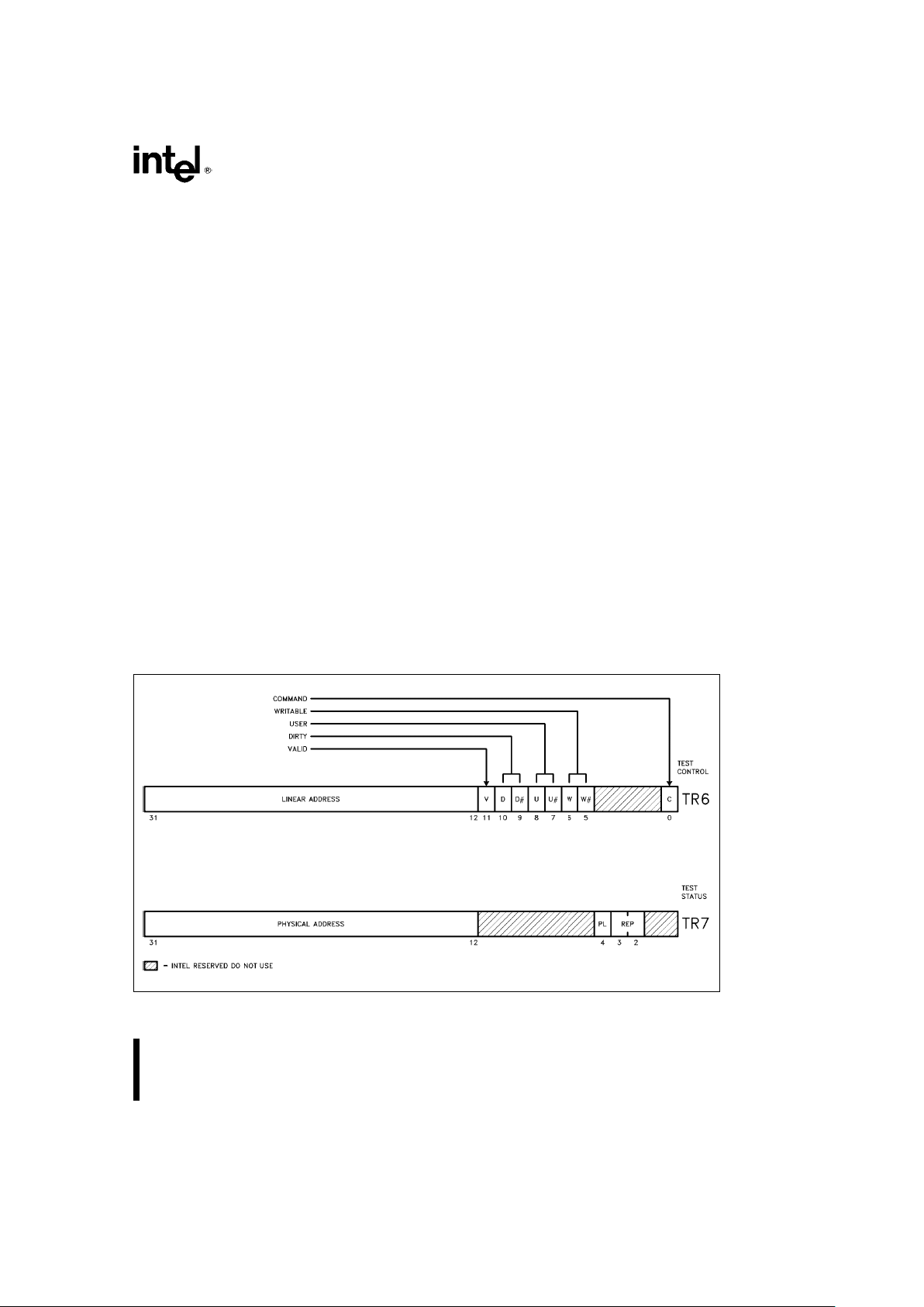
There are two TLB testing operations: 1) writing entries into the TLB, and, 2) performing TLB lookups.
Two Test Registers, shown in Figure 2.6, are provided for the purpose of testing. TR6 is the ‘‘test command register’’, and TR7 is the ‘‘test data register’’.
For a more detailed explanation of testing the TLB,
see the Intel386
TM
SX Microprocessor Program-
mer’s Reference Manual.
2.10 Debugging Support
The Intel386 SX Microprocessor provides several
features which simplify the debugging process. The
three categories of on-chip debugging aids are:
1. The code execution breakpoint opcode (0CCH).
2. The single-step capability provided by the TF bit
in the flag register.
3. The code and data breakpoint capability provided
by the Debug Registers DR0 – 3, DR6, and DR7.
BREAKPOINT INSTRUCTION
A single-byte software interrupt (Int 3) breakpoint instruction is available for use by software debuggers.
The breakpoint opcode is 0CCh, and generates an
exception 3 trap when executed.
SINGLE-STEP TRAP
If the single-step flag (TF, bit 8) in the EFLAG register is found to be set at the end of an instruction, a
single-step exception occurs. The single-step exception is auto vectored to exception number 1.
DEBUG REGISTERS
The Debug Registers are an advanced debugging
feature of the Intel386 SX Microprocessor. They allow data access breakpoints as well as code execution breakpoints. Since the breakpoints are indicated
by on-chip registers, an instruction execution breakpoint can be placed in ROM code or in code shared
by several tasks, neither of which can be supported
by the INT 3 breakpoint opcode.
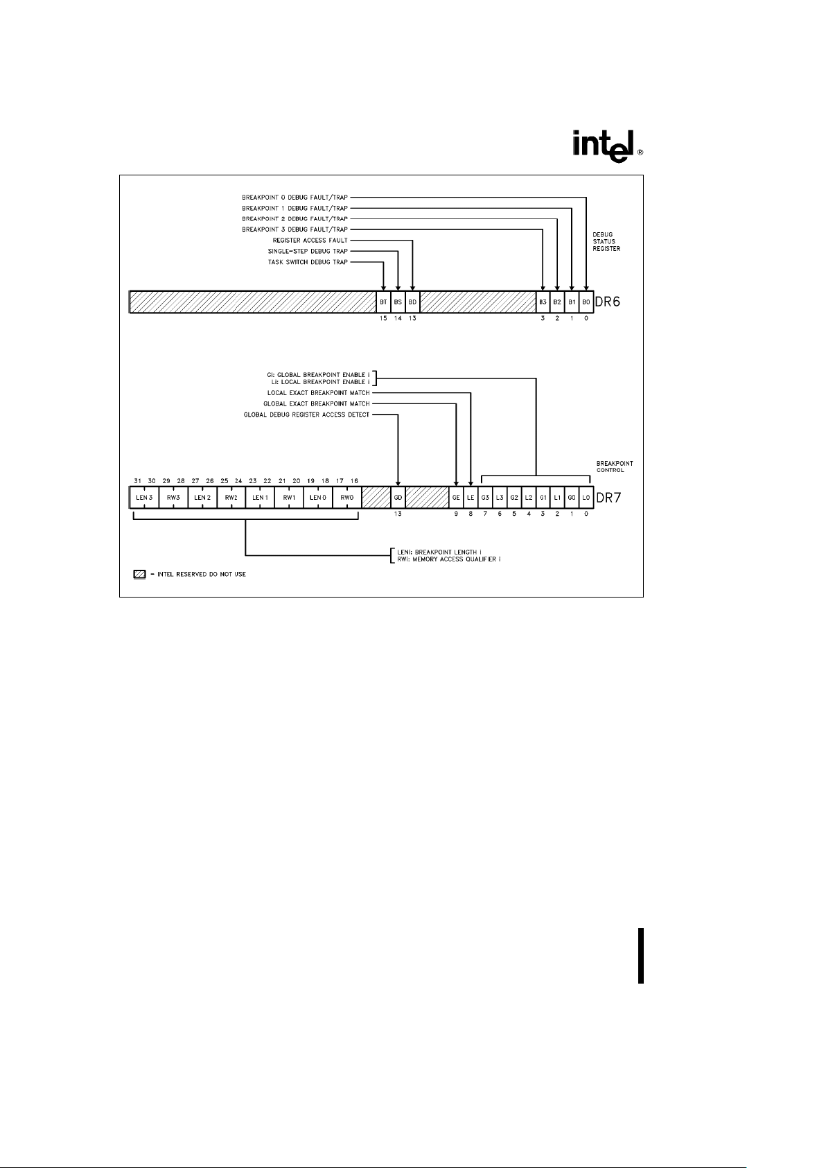
The Intel386 SX Microprocessor contains six Debug
Registers, consisting of four breakpoint address registers and two breakpoint control registers. Initially
after reset, breakpoints are in the disabled state;
therefore, no breakpoints will occur unless the debug registers are programmed. Breakpoints set up in
the Debug Registers are auto-vectored to exception
1. Figure 2.7 shows the breakpoint status and control registers.
240187– 7
Figure 2.6. Test Registers
21
Intel386TMSX MICROPROCESSOR
240187– 8
Figure 2.7. Debug Registers
3.0 REAL MODE ARCHITECTURE
When the processor is reset or powered up it is initialized in Real Mode. Real Mode has the same base
architecture as the 8086, but allows access to the
32-bit register set of the Intel386 SX Microprocessor. The addressing mechanism, memory size, and
interrupt handling are all identical to the Real Mode
on the 80286.
The default operand size in Real Mode is 16 bits, as
in the 8086. In order to use the 32-bit registers and
addressing modes, override prefixes must be used.
In addition, the segment size on the Intel386 SX Microprocessor in Real Mode is 64K bytes so 32-bit
addresses must have a value less then 0000FFFFH.
The primary purpose of Real Mode is to set up the
processor for Protected Mode operation.
3.1 Memory Addressing
In Real Mode the linear addresses are the same as
physical addresses (paging is not allowed). Physical
addresses are formed in Real Mode by adding the
contents of the appropriate segment register which
is shifted left by four bits to an effective address.
This addition results in a 20-bit physical address or a
1 megabyte address space. Since segment registers
are shifted left by 4 bits, Real Mode segments always start on 16-byte boundaries.
All segments in Real Mode are exactly 64K bytes
long, and may be read, written, or executed. The
Intel386 SX Microprocessor will generate an exception 13 if a data operand or instruction fetch occurs
past the end of a segment.
22

Intel386TMSX MICROPROCESSOR
Table 3.1. Exceptions in Real Mode
Function
Interrupt Related Return
Number Instructions Address Location
Interrupt table limit 8 INT vector is not Before
too small within table limit Instruction
CS, DS, ES, FS, GS 13 Word memory reference Before
Segment overrun exception with offset
e
0FFFFH. Instruction
an attempt to execute
past the end of CS segment.
SS Segment overrun 12 Stack Reference Before
exception beyond offset
e
0FFFFH Instruction
3.2 Reserved Locations
There are two fixed areas in memory which are reserved in Real address mode: the system initialization area and the interrupt table area. Locations
00000H through 003FFH are reserved for interrupt
vectors. Each one of the 256 possible interrupts has
a 4-byte jump vector reserved for it. Locations
0FFFFF0H through 0FFFFFFH are reserved for system initialization.
3.3 Interrupts
Many of the exceptions discussed in section 2.7 are
not applicable to Real Mode operation; in particular,
exceptions 10, 11 and 14 do not occur in Real
Mode. Other exceptions have slightly different
meanings in Real Mode; Table 3.1 identifies these
exceptions.
3.4 Shutdown and Halt
The HLT instruction stops program execution and
prevents the processor from using the local bus until
restarted. Either NMI, FLT
Ý
, INTR with interrupts
enabled (IF
e
1), or RESET will force the Intel386 SX
Microprocessor out of halt. If interrupted, the saved
CS:IP will point to the next instruction after the HLT.
Shutdown will occur when a severe error is detected
that prevents further processing. In Real Mode,
shutdown can occur under two conditions:
1. An interrupt or an exception occurs (Exceptions 8
or 13) and the interrupt vector is larger than the
Interrupt Descriptor Table.
2. A CALL, INT or PUSH instruction attempts to
wrap around the stack segment when SP is not
even.
An NMI input can bring the processor out of shutdown if the Interrupt Descriptor Table limit is large
enough to contain the NMI interrupt vector (at least
000FH) and the stack has enough room to contain
the vector and flag information (i.e. SP is greater that
0005H). Otherwise, shutdown can only be exited by
a processor reset.
3.5 LOCK Operation
The LOCK prefix on the Intel386 SX Microprocessor,
even in Real Mode, is more restrictive than on the
80286. This is due to the addition of paging on the
Intel386 SX Microprocessor in Protected Mode and
Virtual 8086 Mode. The LOCK prefix is not supported during repeat string instructions.
The only instruction forms where the LOCK prefix is
legal on the Intel386 SX Microprocessor are shown
in Table 3.2.
Table 3.2. Legal Instructions for the LOCK Prefix
Opcode
Operands
(Dest, Source)
BIT Test and
SET/RESET Mem, Reg/Immediate
/COMPLEMENT
XCHG Reg, Mem
XCHG Mem, Reg
ADD, OR, ADC, SBB,
AND, SUB, XOR Mem, Reg/Immediate
NOT, NEG, INC, DEC Mem
An exception 6 will be generated if a LOCK prefix is
placed before any instruction form or opcode not
listed above. The LOCK prefix allows indivisible
read/modify/write operations on memory operands
using the instructions above.
The LOCK prefix is not IOPL-sensitive on the
Intel386 SX Microprocessor. The LOCK prefix can
be used at any privilege level, but only on the instruction forms listed in Table 3.2.
23

Intel386TMSX MICROPROCESSOR
4.0 PROTECTED MODE
ARCHITECTURE
The complete capabilities of the Intel386 SX Microprocessor are unlocked when the processor operates in Protected Virtual Address Mode (Protected
Mode). Protected Mode vastly increases the linear
address space to four gigabytes (232bytes) and allows the running of virtual memory programs of almost unlimited size (64 terabytes (2
46
bytes)). In addition, Protected Mode allows the Intel386 SX Microprocessor to run all of the existing Intel386 DX CPU
(using only 16 megabytes of physical memory),
80286 and 8086 CPU’s software, while providing a
sophisticated memory management and a hardware-assisted protection mechanism. Protected
Mode allows the use of additional instructions specially optimized for supporting multitasking operating
systems. The base architecture of the Intel386 SX
Microprocessor remains the same; the registers, instructions, and addressing modes described in the
previous sections are retained. The main difference
between Protected Mode and Real Mode from a
programmer’s viewpoint is the increased address
space and a different addressing mechanism.
4.1 Addressing Mechanism
Like Real Mode, Protected Mode uses two components to form the logical address; a 16-bit selector is
used to determine the linear base address of a segment, the base address is added to a 32-bit effective
address to form a 32-bit linear address. The linear
address is then either used as a 24-bit physical address, or if paging is enabled the paging mechanism
maps the 32-bit linear address into a 24-bit physical
address.
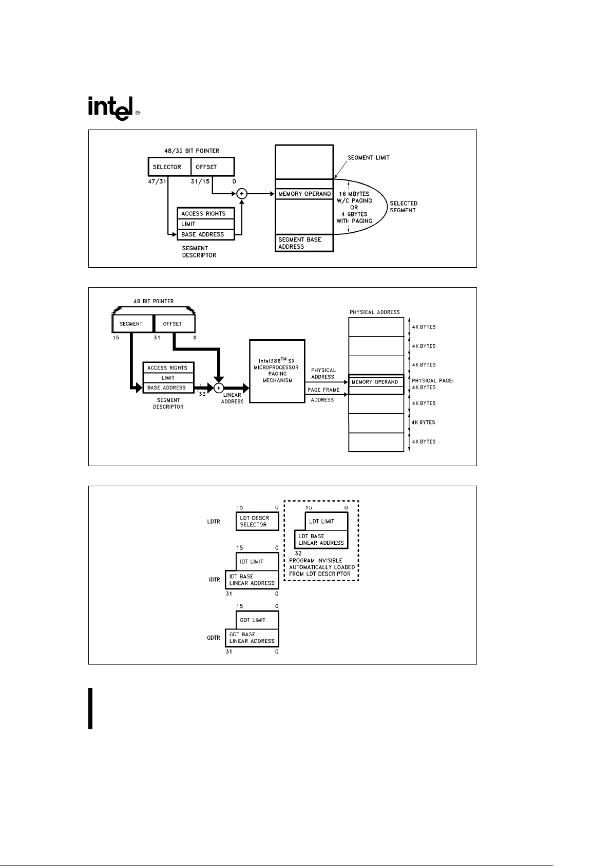
The difference between the two modes lies in calculating the base address. In Protected Mode, the selector is used to specify an index into an operating
system defined table (see Figure 4.1). The table
contains the 32-bit base address of a given segment. The physical address is formed by adding the
base address obtained from the table to the offset.
Paging provides an additional memory management
mechanism which operates only in Protected Mode.
Paging provides a means of managing the very large
segments of the Intel386 SX Microprocessor, as
paging operates beneath segmentation. The page
mechanism translates the protected linear address
which comes from the segmentation unit into a
physical address. Figure 4.2 shows the complete Intel386 SX Microprocessor addressing mechanism
with paging enabled.
4.2 Segmentation
Segmentation is one method of memory management. Segmentation provides the basis for protection. Segments are used to encapsulate regions of
memory which have common attributes. For example, all of the code of a given program could be contained in a segment, or an operating system table
may reside in a segment. All information about each
segment is stored in an 8 byte data structure called
a descriptor. All of the descriptors in a system are
contained in descriptor tables which are recognized
by hardware.
TERMINOLOGY
The following terms are used throughout the discussion of descriptors, privilege levels and protection:
PL: Privilege LevelÐOne of the four hierarchical
privilege levels. Level 0 is the most privileged
level and level 3 is the least privileged.
RPL: Requestor Privilege LevelÐThe privilege level
of the original supplier of the selector. RPL is
determined by the least two significant bits of
a selector.
DPL: Descriptor Privilege LevelÐThis is the least
privileged level at which a task may access
that descriptor (and the segment associated
with that descriptor). Descriptor Privilege Level is determined by bits 6:5 in the Access
Right Byte of a descriptor.
CPL: Current Privilege LevelÐThe privilege level at
which a task is currently executing, which
equals the privilege level of the code segment
being executed. CPL can also be determined
by examining the lowest 2 bits of the CS register, except for conforming code segments.
EPL: Effective Privilege LevelÐThe effective privi-
lege level is the least privileged of the RPL
and the DPL. EPL is the numerical maximum
of RPL and DPL.
Task: One instance of the execution of a program.
Tasks are also referred to as processes.
DESCRIPTOR TABLES
The descriptor tables define all of the segments
which are used in a Intel386 SX Microprocessor system. There are three types of tables which hold descriptors: the Global Descriptor Table, Local Descriptor Table, and the Interrupt Descriptor Table. All
of the tables are variable length memory arrays and
can vary in size from 8 bytes to 64K bytes. Each
table can hold up to 8192 8-byte descriptors. The
upper 13 bits of a selector are used as an index into
the descriptor table. The tables have registers associated with them which hold the 32-bit linear base
address and the 16-bit limit of each table.
24
Intel386TMSX MICROPROCESSOR
240187– 9
Figure 4.1. Protected Mode Addressing
240187– 10
Figure 4.2. Paging and Segmentation
240187– 11
Figure 4.3. Descriptor Table Registers
25
Intel386TMSX MICROPROCESSOR
Each of the tables has a register associated with it:
GDTR, LDTR, and IDTR; see Figure 2.1. The LGDT,
LLDT, and LIDT instructions load the base and limit
of the Global, Local, and Interrupt Descriptor Tables
into the appropriate register. The SGDT, SLDT, and
SIDT store the base and limit values. These are privileged instructions.
Global Descriptor Table
The Global Descriptor Table (GDT) contains descriptors which are available to all of the tasks in a
system. The GDT can contain any type of segment
descriptor except for interrupt and trap descriptors.
Every Intel386 SX CPU system contains a GDT.
The first slot of the Global Descriptor Table corresponds to the null selector and is not used. The null
selector defines a null pointer value.
Local Descriptor Table
LDTs contain descriptors which are associated with
a given task. Generally, operating systems are designed so that each task has a separate LDT. The
LDT may contain only code, data, stack, task gate,
and call gate descriptors. LDTs provide a mechanism for isolating a given task’s code and data segments from the rest of the operating system, while
the GDT contains descriptors for segments which
are common to all tasks. A segment cannot be accessed by a task if its segment descriptor does not
exist in either the current LDT or the GDT. This provides both isolation and protection for a task’s segments while still allowing global data to be shared
among tasks.
Unlike the 6-byte GDT or IDT registers which contain
a base address and limit, the visible portion of the
LDT register contains only a 16-bit selector. This selector refers to a Local Descriptor Table descriptor in
the GDT (see figure 2.1).
Interrupt Descriptor Table
The third table needed for Intel386 SX Microprocessor systems is the Interrupt Descriptor Table. The
IDT contains the descriptors which point to the location of the up to 256 interrupt service routines. The
IDT may contain only task gates, interrupt gates, and
trap gates. The IDT should be at least 256 bytes in
size in order to hold the descriptors for the 32 Intel
Reserved Interrupts. Every interrupt used by a system must have an entry in the IDT. The IDT entries
are referenced by INT instructions, external interrupt
vectors, and exceptions.
DESCRIPTORS
The object to which the segment selector points to
is called a descriptor. Descriptors are eight byte
quantities which contain attributes about a given region of linear address space. These attributes include the 32-bit base linear address of the segment,
the 20-bit length and granularity of the segment, the
protection level, read, write or execute privileges,
the default size of the operands (16-bit or 32-bit),
and the type of segment. All of the attribute information about a segment is contained in 12 bits in the
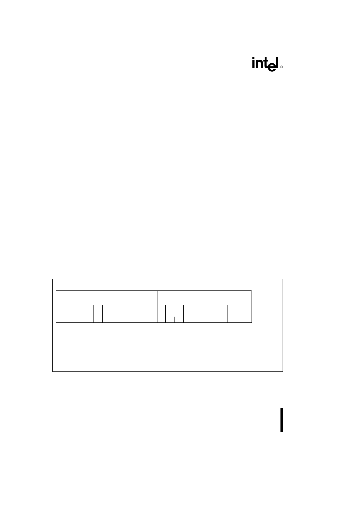
segment descriptor. Figure 4.4 shows the general
format of a descriptor. All segments on the Intel386
SX Microprocessor have three attribute fields in
common: the P bit, the DPL bit, and the S bit. The P
31 0 BYTE
SEGMENT BASE 15...0 SEGMENT LIMIT 15...0
ADDRESS
0
BASE 31...24 G D 0 AVL
LIMIT
P DPL S TYPE A
BASE
a
4
19...16 23...16
BASE Base Address of the segment
LIMIT The length of the segment
P Present Bit 1
e
Present 0eNot Present
DPL Descriptor Privilege Level 0 –3
S Segment Descriptor 0
e
System Descriptor 1eCode or Data Segment Descriptor
TYPE Type of Segment
A Accessed Bit
G Granularity Bit 1
e
Segment length is page granular 0eSegment length is byte granular
D Default Operation Size (recognized in code segment descriptors only) 1
e
32-bit segment 0e16-bit segment
0 Bit must be zero (0) for compatibility with future processors
AVL Available field for user or OS
Figure 4.4. Segment Descriptors
26

Intel386TMSX MICROPROCESSOR
(Present) Bit is 1 if the segment is loaded in physical
memory. If P
e
0 then any attempt to access this
segment causes a not present exception (exception
11). The Descriptor Privilege Level, DPL, is a two bit
field which specifies the protection level, 0 – 3, associated with a segment.
The Intel386 SX Microprocessor has two main categories of segments: system segments and non-system segments (for code and data). The segment bit,
S, determines if a given segment is a system seg-
ment or a code or data segment. If the S bit is 1 then
the segment is either a code or data segment; if it is
0 then the segment is a system segment.
Code and Data Descriptors (S
e
1)
Figure 4.5 shows the general format of a code and
data descriptor and Table 4.1 illustrates how the bits
in the Access Right Byte are interpreted.
31 0
SEGMENT BASE 15...0 SEGMENT LIMIT 15...0 0
LIMIT
ACCESS BASE
BASE 31...24 G D 0 AVL
19...16
RIGHTS
23...16
a
4
BYTE
D/B 1eDefault Instructions Attributes are 32-Bits
0
e
Default Instruction Attributes are 16-Bits
AVL Available field for user or OS
G Granularity Bit 1
e
Segment length is page granular
0
e
Segment length is byte granular
0 Bit must be zero (0) for compatibility with future processors
Figure 4.5. Code and Data Descriptors
Table 4.1. Access Rights Byte Definition for Code and Data Descriptors
Bit
Name Function
Position
7 Present (P) Pe1 Segment is mapped into physical memory.
P
e
0 No mapping to physical memory exists, base and limt are
not used.
6–5 Descriptor Privilege Segment privilege attribute used in privilege tests.
Level (DPL)
4 Segment Descrip- S
e
1 Code or Data (includes stacks) segment descriptor
tor (S) S
e
0 System Segment Descriptor or Gate Descriptor
3 Executable (E) Ee0 Descriptor type is data segment: If
2 Expansion Direc- ED
e
0 Expand up segment, offsets must beslimit. Data
tion (ED) ED
e
1 Expand down segment, offsets must bellimit. Segment
1 Writeable (W) W
e
0 Data segment may not be written into. (Se1,
W
e
1 Data segment may be written into. *E
e
0)
3 Executable (E) Ee1 Descriptor type is code segment: If
2 Conforming (C) C
e
1 Code segment may only be executed Code
when CPL
t
DPL and CPL Segment
remains unchanged. (S
e
1,
1 Readable (R) R
e
0 Code segment may not be read. Ee1)
R
e
1 Code segment may be read. *
0 Accessed (A) Ae0 Segment has not been accessed.
A
e
1 Segment selector has been loaded into segment register
or used by selector test instructions.
27
Intel386TMSX MICROPROCESSOR
31 16 0
SEGMENT BASE 15...0 SEGMENT LIMIT 15...0 0
BASE 31...24 G 0 0 0
LIMIT
P DPL 0 TYPE
BASE
a
4
19...16 23...16
Type Defines
0 Invalid
1 Available 80286 TSS
2 LDT
3 Busy 80286 TSS
4 80286 Call Gate
5 Task Gate (for 80286 or Intel386
TM
SX
Microprocessor Task)
6 80286 Interrupt Gate
7 80286 Trap Gate
Type Defines
8 Invalid
9 Available Intel386
TM
SX Microprocessor TSS
A Undefined (Intel Reserved)
B Busy Intel386
TM
SX Microprocessor TSS
C Intel386
TM
SX Microprocessor Call Gate
D Undefined (Intel Reserved)
E Intel386
TM
SX Microprocessor Interrupt Gate
F Intel386
TM
SX Microprocessor Trap Gate
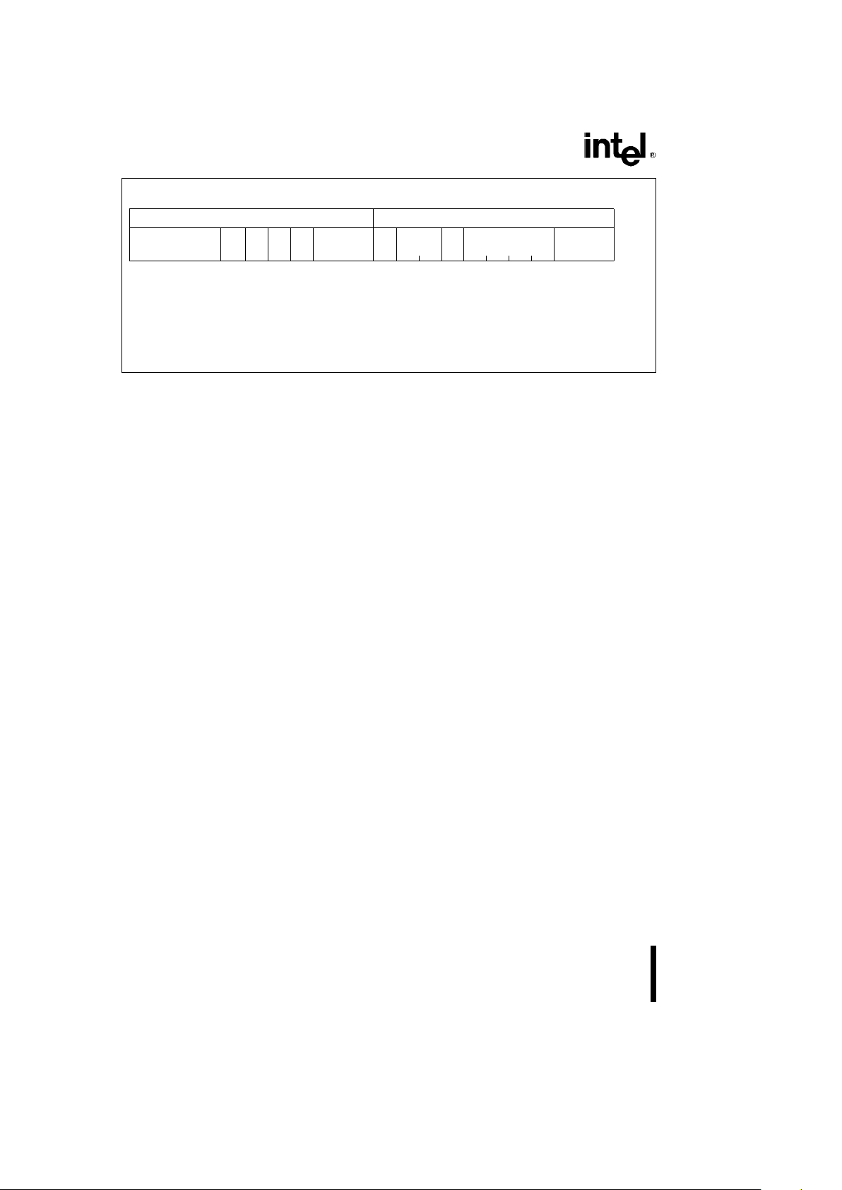
Figure 4.6. System Descriptors
Code and data segments have several descriptor
fields in common. The accessed bit, A, is set whenever the processor accesses a descriptor. The granularity bit, G, specifies if a segment length is bytegranular or page-granular.
System Descriptor Formats (S
e
0)
System segments describe information about operating system tables, tasks, and gates. Figure 4.6
shows the general format of system segment descriptors, and the various types of system segments.
Intel386 SX system descriptors (which are the same
as Intel386 DX CPU system descriptors) contain a
32-bit base linear address and a 20-bit segment limit. 80286 system descriptors have a 24-bit base address and a 16-bit segment limit. 80286 system descriptors are identified by the upper 16 bits being all
zero.
Differences Between Intel386
TM
SX
Microprocessor and 80286 Descriptors
In order to provide operating system compatibility
with the 80286 the Intel386 SX CPU supports all of
the 80286 segment descriptors. The 80286 system
segment descriptors contain a 24-bit base address
and 16-bit limit, while the Intel386 SX CPU system
segment descriptors have a 32-bit base address, a
20-bit limit field, and a granularity bit. The word count
field specifies the number of 16-bit quantities to copy
for 80286 call gates and 32-bit quantities for
Intel386 SX CPU call gates.
Selector Fields
A selector in Protected Mode has three fields: Local
or Global Descriptor Table indicator (TI), Descriptor
Entry Index (Index), and Requestor (the selector’s)
Privilege Level (RPL) as shown in Figure 4.7. The TI
bit selects either the Global Descriptor Table or the
Local Descriptor Table. The Index selects one of 8k
descriptors in the appropriate descriptor table. The
RPL bits allow high speed testing of the selector’s
privilege attributes.
Segment Descriptor Cache
In addition to the selector value, every segment register has a segment descriptor cache register associated with it. Whenever a segment register’s contents are changed, the 8-byte descriptor associated
with that selector is automatically loaded (cached)
on the chip. Once loaded, all references to that segment use the cached descriptor information instead
of reaccessing the descriptor. The contents of the
descriptor cache are not visible to the programmer.
Since descriptor caches only change when a segment register is changed, programs which modify
the descriptor tables must reload the appropriate
segment registers after changing a descriptor’s value.
28
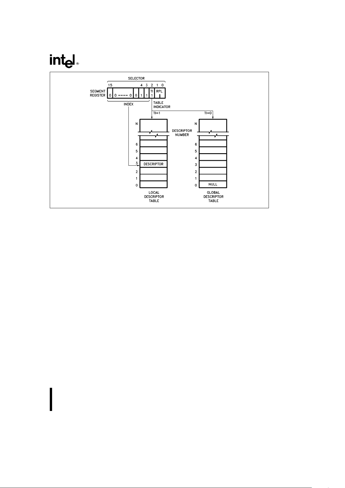
Intel386TMSX MICROPROCESSOR
240187– 12
Figure 4.7. Example Descriptor Selection
4.3 Protection
The Intel386 SX Microprocessor has four levels of
protection which are optimized to support a multitasking operating system and to isolate and protect
user programs from each other and the operating
system. The privilege levels control the use of privileged instructions, I/O instructions, and access to
segments and segment descriptors. The Intel386 SX
Microprocessor also offers an additional type of protection on a page basis when paging is enabled.
The four-level hierarchical privilege system is an extension of the user/supervisor privilege mode commonly used by minicomputers. The user/supervisor
mode is fully supported by the Intel386 SX Microprocessor paging mechanism. The privilege levels
(PL) are numbered 0 through 3. Level 0 is the most
privileged level.
RULES OF PRIVILEGE
The Intel386 SX Microprocessor controls access to
both data and procedures between levels of a task,
according to the following rules.
Ð Data stored in a segment with privilege level p
can be accessed only by code executing at a
privilege level at least as privileged as p.
Ð A code segment/procedure with privilege level p
can only be called by a task executing at the
same or a lesser privilege level than p.
PRIVILEGE LEVELS
At any point in time, a task on the Intel386 SX Microprocessor always executes at one of the four privilege levels. The Current Privilege Level (CPL) specifies what the task’s privilege level is. A task’s CPL
may only be changed by control transfers through
gate descriptors to a code segment with a different
privilege level. Thus, an application program running
at PL
e
3 may call an operating system routine at
PL
e
1 (via a gate) which would cause the task’s CPL
to be set to 1 until the operating system routine was
finished.
Selector Privilege (RPL)
The privilege level of a selector is specified by the
RPL field. The selector’s RPL is only used to establish a less trusted privilege level than the current
privilege level of the task for the use of a segment.
This level is called the task’s effective privilege level
(EPL). The EPL is defined as being the least privileged (numerically larger) level of a task’s CPL and a
selector’s RPL. The RPL is most commonly used to
verify that pointers passed to an operating system
procedure do not access data that is of higher privilege than the procedure that originated the pointer.
Since the originator of a selector can specify any
RPL value, the Adjust RPL (ARPL) instruction is provided to force the RPL bits to the originator’s CPL.
29

Intel386TMSX MICROPROCESSOR
Table 4.2. Descriptor Types Used for Control Transfer
Control Transfer Types Operation Types
Descriptor Descriptor
Referenced Table
Intersegment within the same privilege level JMP, CALL RET, IRET* Code Segment GDT/LDT
Intersegment to the same or higher privilege level CALL Call Gate GDT/LDT
Interrupt within task may change CPL
Interrupt instruction Trap or IDT
Exception External Interrupt
Interrupt Gate
Intersegment to a lower privilege level RET, IRET* Code Segment GDT/LDT
(changes task CPL)
CALL, JMP Task State GDT
Segment
Task Switch CALL, JMP Task Gate GDT/LDT
IRET** Task Gate IDT
Interrupt instruction,
Exception, External
Interrupt
*NT (Nested Task bit of flag register)e0
**NT (Nested Task bit of flag register)
e
1
I/O Privilege
The I/O privilege level (IOPL) lets the operating system code executing at CPL
e
0 define the least privileged level at which I/O instructions can be used. An
exception 13 (General Protection Violation) is generated if an I/O instruction is attempted when the CPL
of the task is less privileged then the IOPL. The
IOPL is stored in bits 13 and 14 of the EFLAGS register. The following instructions cause an exception
13 if the CPL is greater than IOPL: IN, INS, OUT,
OUTS, STI, CLI, LOCK prefix.
Descriptor Access
There are basically two types of segment accesses:
those involving code segments such as control
transfers, and those involving data accesses. Determining the ability of a task to access a segment involves the type of segment to be accessed, the instruction used, the type of descriptor used and CPL,
RPL, and DPL as described above.
Any time an instruction loads a data segment register (DS, ES, FS, GS) the Intel386 SX Microprocessor
makes protection validation checks. Selectors loaded in the DS, ES, FS, GS registers must refer only to
data segment or readable code segments.
Finally the privilege validation checks are performed.
The CPL is compared to the EPL and if the EPL is
more privileged than the CPL, an exception 13 (general protection fault) is generated.
The rules regarding the stack segment are slightly
different than those involving data segments. Instructions that load selectors into SS must refer to
data segment descriptors for writeable data segments. The DPL and RPL must equal the CPL of all
other descriptor types or a privilege level violation
will cause an exception 13. A stack not present fault
causes an exception 12.
PRIVILEGE LEVEL TRANSFERS
Inter-segment control transfers occur when a selector is loaded in the CS register. For a typical system
most of these transfers are simply the result of a call
or a jump to another routine. There are five types of
control transfers which are summarized in Table 4.2.
Many of these transfers result in a privilege level
transfer. Changing privilege levels is done only by
control transfers, using gates, task switches, and interrupt or trap gates.
Control transfers can only occur if the operation
which loaded the selector references the correct descriptor type. Any violation of these descriptor usage
rules will cause an exception 13.
30
