Intel Corporation iMC020FLSA-ET15, iMC020FLSA-15, iMC010FLSA-ET15, iMC010FLSA-15, iMC004FLSA-ET15 Datasheet
...
December 1996 Order Number: 290434-006
SERIES 2 FLASH MEMORY CARDS
iMC002FLSA, iMC004FLSA, iMC010FLSA, iMC020FLSA
Extended Temperature Specifications Included
Y
2, 4, 10 and 20 Megabyte Capacities
Y
PCMCIA 2.1/JEIDA 4.1 68-Pin Standard
Ð Hardwired Card Information
Structure
Ð Byte- or Word-Wide Selectable
Y
Component Management Registers for
Card Status/Control and Flexible
System Interface
Y
Automatic Erase/Write
Ð Monitored with Ready/Busy Output
Y
Card Power-Down Modes
Ð Deep-Sleep for Low Power
Applications
Y
Mechanical Write Protect Switch
Y
Solid-State Reliability
Y
Intel FlashFileTMArchitecture
Y
High-Performance Read Access
Ð 150 ns Maximum
Y
High-Performance Random Writes
Ð6 ms Typical Word Write
Y
Erase Suspend to Read Command
Ð Keeps Erase as Background Task
Y
Nonvolatility (Zero Retention Power)
Ð No Batteries Required for Back-up
Y
ETOXTMV 0.4m Flash Memory
Technology
Ð 5V Read, 12V Erase/Write
Ð High-Volume Manufacturing
Experience
Y
Extended Temperature Version
Ð
b
40§Ctoa85§C
Intel’s Series 2 Flash Memory Card facilitates high-performance disk emulation in mobile PCs and dedicated
equipment. Manufactured with Intel’s ETOX
TM
III 0.8m, FlashFile Memory devices, the Series 2 Card allows
code and data retention while erasing and/or writing other blocks. Additionally, the Series 2 Flash Memory
Card features low power modes, flexible system interfacing and a 150 ns read access time. When coupled with
Intel’s low-power microprocessors, these cards enable high-performance implementations of mobile computers and systems.
Series 2 Cards conform to the Personal Computer Memory Card International Association (PCMCIA 2.1)/Japanese Electronics Industry Development Association (JEIDA 4.1) 68-pin standard, providing electrical and
physical compatibility.
Data file management software, Flash Translation Layer (FTL), provides data file storage and memory management, much like a disk operating system. Intel’s Series 2 Flash Memory Cards, coupled with flash file
management software, effectively provide a removable, all-silicon mass storage solution with higher performance and reliability than disk-based memory architectures.
Designing with Intel’s FlashFile Architecture enables OEM system manufacturers to design and manufacture a
new generation of mobile PCs and dedicated equipment where high performance, ruggedness, long battery
life and lighter weight are a requirement. For large user groups in workstation environments, the Series 2
Cards provide a means to securely store user data and backup system configuration/status information.
SERIES 2 FLASH MEMORY CARDS
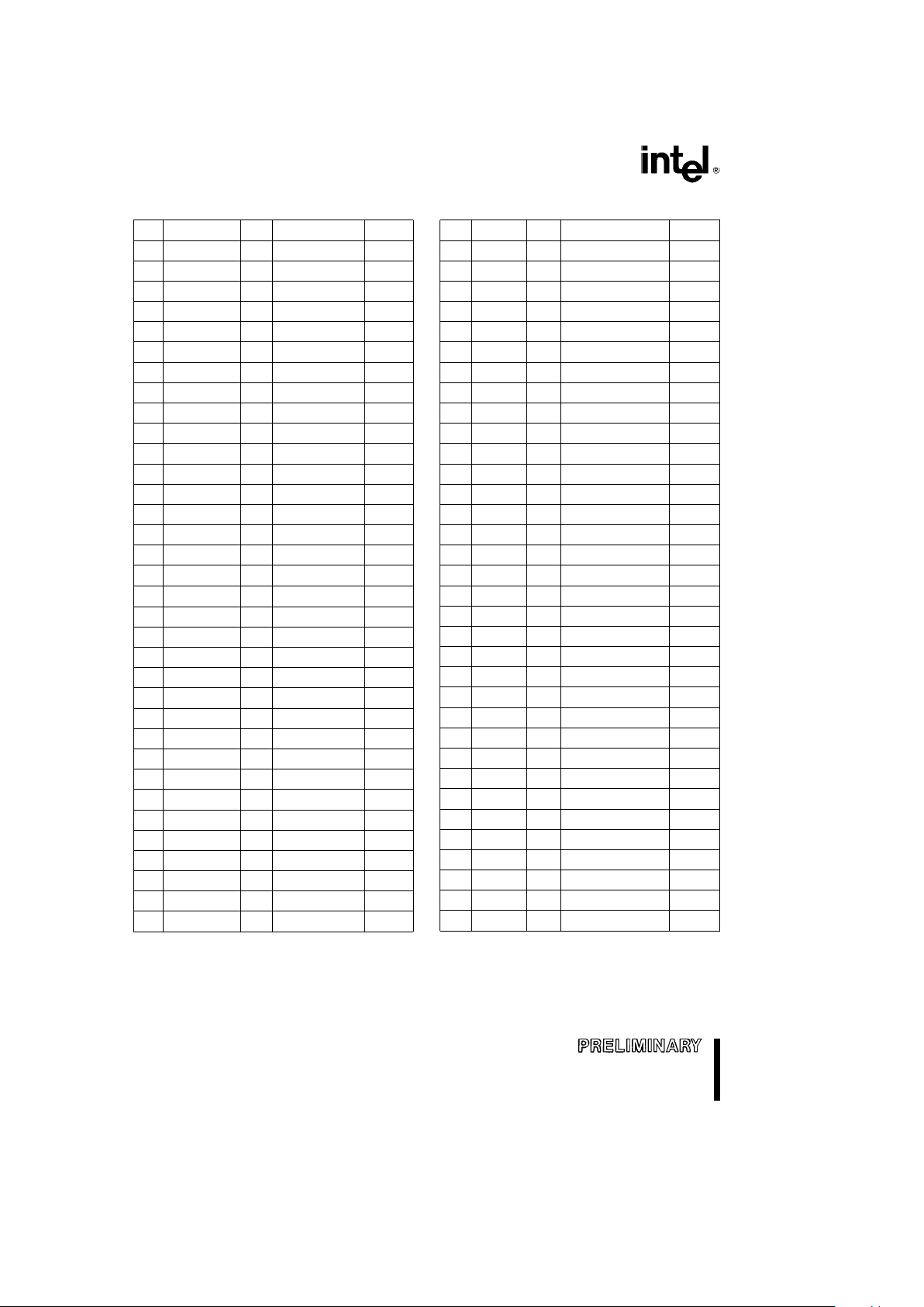
Table 1. Series 2 Flash Memory Card Pinout
Pin Signal I/O Function Active
1 GND Ground
2DQ
3
I/O Data Bit 3
3DQ
4
I/O Data Bit 4
4DQ
5
I/O Data Bit 5
5DQ
6
I/O Data Bit 6
6DQ
7
I/O Data Bit 7
7CE
1
Ý
I Card Enable 1 LO
8A
10
I Address Bit 10
9OE
Ý
I Output Enable LO
10 A
11
I Address Bit 11
11 A
9
I Address Bit 9
12 A
8
I Address Bit 8
13 A
13
I Address Bit 13
14 A
14
I Address Bit 14
15 WE
Ý
I Write Enable LO
16 RDY/BSY
Ý
Ready-Busy HI/LO
17 V
CC
Supply Voltage
18 V
PP1
Supply Voltage
19 A
16
I Address Bit 16
20 A
15
I Address Bit 15
21 A
12
I Address Bit 12
22 A
7
I Address Bit 7
23 A
6
I Address Bit 6
24 A
5
I Address Bit 5
25 A
4
I Address Bit 4
26 A
3
I Address Bit 3
27 A
2
I Address Bit 2
28 A
1
I Address Bit 1
29 A
0
I Address Bit 0
30 DQ
0
I/O Data Bit 0
31 DQ
1
I/O Data Bit 1
32 DQ
2
I/O Data Bit 2
33 WP O Write Protect HI
34 GND Ground
Pin Signal I/O Function Active
35 GND Ground
36 CD
1
Ý
O Card Detect 1 LO
37 DQ
11
I/O Data Bit 11
38 DQ
12
I/O Data Bit 12
39 DQ
13
I/O Data Bit 13
40 DQ
14
I/O Data Bit 14
41 DQ
15
I/O Data Bit 15
42 CE
2
Ý
I Card Enable 2 LO
43 VS
1
O Voltage Sense 1 N.C.
44 RFU Reserved
45 RFU Reserved
46 A
17
I Address Bit 17
47 A
18
I Address Bit 18
48 A
19
I Address Bit 19
49 A
20
I Address Bit 20
50 A
21
I Address Bit 21
51 V
CC
Supply Voltage
52 V
PP2
Supply Voltage
53 A
22
I Address Bit 22
54 A
23
I Address Bit 23
55 A
24
I Address Bit 24
56 A
25
No Connect
57 VS
2
O Voltage Sense 2 N.C.
58 RST I Reset HI
59 WAITÝO Extend Bus Cycle LO
60 RFU Reserved
61 REG
Ý
I Register Select LO
62 BVD
2
O Batt. Volt Det 2
63 BVD
1
O Batt. Volt Det 1
64 DQ
8
I/O Data Bit 8
65 DQ
9
I/O Data Bit 9
66 DQ
10
I/O Data Bit 10
67 CD
2
Ý
O Card Detect 2 LO
68 GND Ground
2

SERIES 2 FLASH MEMORY CARDS
Table 2. Series 2 Flash Memory Card Pin Descriptions
Symbol Type Name and Function
A0–A
25
I ADDRESS INPUTS: A0through A25are address bus lines which enable direct
addressing of 64 megabytes of memory on a card. A
0
is not used in word
access mode. A
24
is the most significant address bit. Note: A25is a no-connect
but should be provided on host side.
DQ0–DQ
15
I/O DATA INPUT/OUTPUT: DQ0through DQ15constitute the bidirectional data
bus. DQ15is the most significant bit.
CE
1
Ý
,CE
2
Ý
I CARD ENABLE 1, 2: CE
1
Ý
enables even bytes, CE
2
Ý
enables odd bytes.
Multiplexing A
0
,CE
1
Ý
and CE
2
Ý
allows 8-bit hosts to access all data on DQ
0
through DQ7. (See Table 3 for a more detailed description.)
OE
Ý
I OUTPUT ENABLE: Active low signal gating read data from the memory card.
WE
Ý
I WRITE ENABLE: Active low signal gating write data to the memory card.
RDY/BSY
Ý
O READY/BUSY OUTPUT: Indicates status of internally timed erase or write
activities. A high output indicates the memory card is ready to accept
accesses. A low output indicates that a device(s) in the memory card is(are)
busy with internally timed activities. See text for an alternate function (READYBUSY MODE REGISTER).
CD
1
Ý
&CD
2
Ý
O CARD DETECT 1, 2: These signals provide for correct card insertion detection.
They are positioned at opposite ends of the card to detect proper alignment.
The signals are connected to ground internally on the memory card and will be
forced low whenever a card is placed in the socket. The host socket interface
circuitry shall supply 10K or larger pull-up resistors on these signal pins.
WP O WRITE PROTECT: Write Protect reflects the status of the Write-Protect switch
on the memory card. WP set high
e
write protected, providing internal
hardware write lockout to the flash array.
V
PP1,VPP2
WRITE/ERASE POWER SUPPLY: (12V nominal) for erasing memory array
blocks or writing data in the array. They must be 12V to perform an erase/write
operation.
V
CC
CARD POWER SUPPLY (5V nominal) for all internal circuitry.
GND I GROUND for all internal circuitry.
REG
Ý
I REGISTER SELECT provides access to Series 2 Flash Memory Card registers
and Card Information Structure in the Attribute Memory Plane.
RST I RESET from system, active high. Places card in Power-On Default State.
RESET pulse width must be
t
200 ns.
WAIT
Ý
O WAIT (Extend Bus Cycle) is used by Intel’s I/O cards and is driven high.
BVD1, BVD
2
O BATTERY VOLTAGE DETECT: Upon completion of the power on reset cycle,
these signals are driven high to maintain SRAM-card compatibility.
RFU RESERVED FOR FUTURE USE
NC NO INTERNAL CONNECTION. Pin may be driven or left floating.
VS1,VS
2
VOLTAGE SENSE: Notifies the host Socket of the card’s VCCrequirements.
VS
1
and VS2are both open, indicating a 5V VCCcard.
3
SERIES 2 FLASH MEMORY CARDS
290434– 3
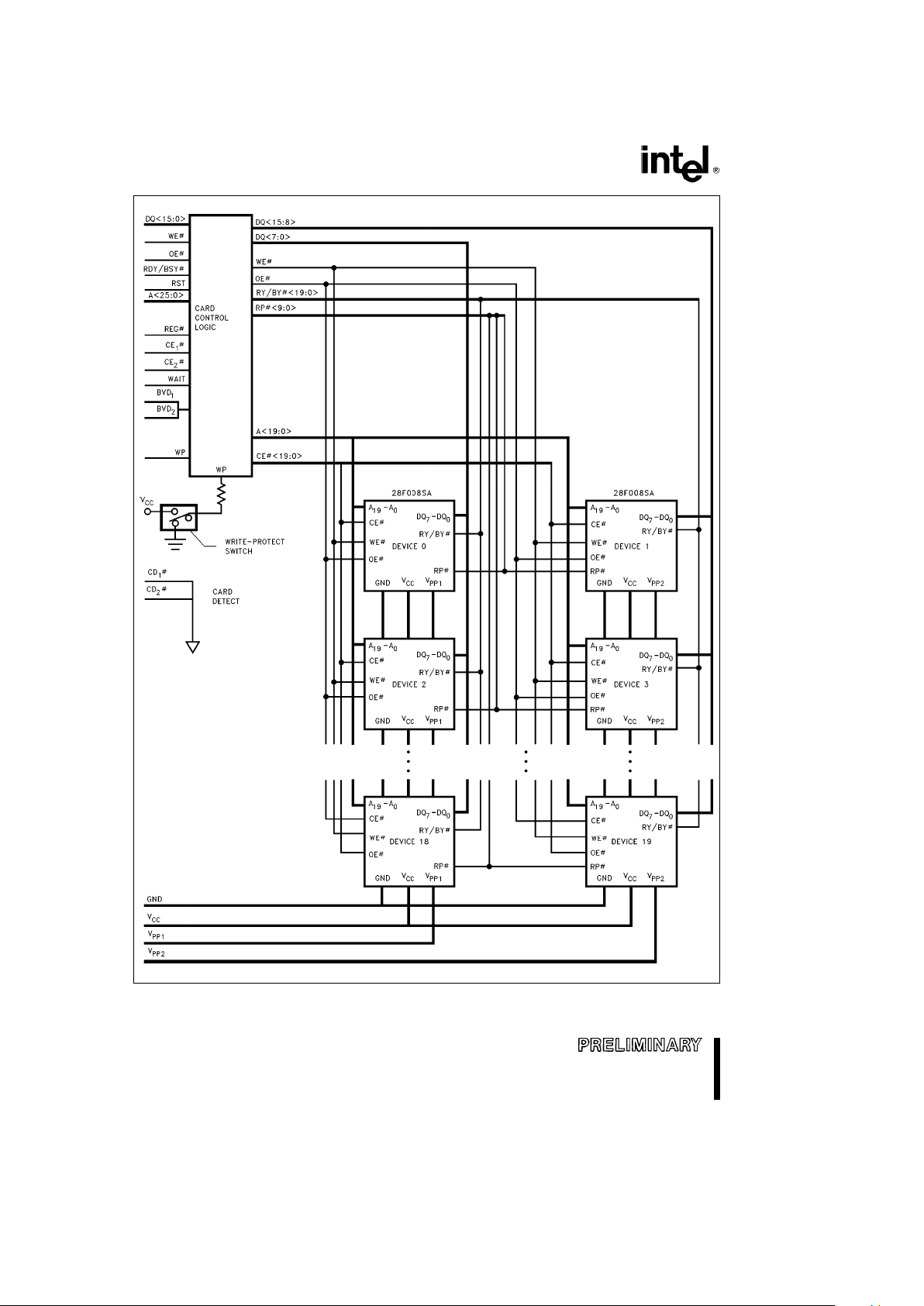
Figure 1. Detailed Block Diagram. The Card Control Logic Provides
Decoding Buffering and Control Signals.
4

SERIES 2 FLASH MEMORY CARDS
APPLICATIONS
Intel’s second generation Series 2 Flash Memory
Cards facilitate high performance disk emulation for
the storage of data files and application programs on
a purely solid-state removable medium. File management software, Flash Translation Layer (FTL), in
conjunction with the Series 2 Flash Memory Cards,
enable the design of high-performance light-weight
notebook, palmtop, and pen-based PCs that have
the processing power of today’s desktop computers.
Application software stored on the flash memory
card substantially reduces the slow disk-to-DRAM
download process. Replacing the mechanical disk
results in a dramatic enhancement of read performance and substantial reduction of power consumption, size and weightÐconsiderations particularly
important in portable PCs and equipment. The Series 2 Card’s high performance read access time allows the use of Series 2 Cards in an ‘‘execute-inplace’’ (XIP) architecture. XIP eliminates redundancy
associated with DRAM/Disk memory system architectures. Operating systems stored in Flash Memory
decreases system boot or program load times, enabling the design of PCs that boot, operate, store
data files and execute application programs from/to
nonvolatile memory without losing the ability to perform an update.
File management systems modify and store data
files by allocating flash memory space intelligently.
Wear leveling algorithms, employed to equally distribute the number of rewrite cycles, ensure that no
particular block is cycled excessively relative to other blocks. This provides hundreds of thousands of
hours of power on usage.
This file management software enables the user to
interact with the flash memory card in precisely the
same way as a magnetic disk.
Series 2 Flash Memory Cards provide durable nonvolatile memory storage for mobile PCs on the road,
facilitating simple transfer back into the desktop environment.
For systems currently using a static RAM/battery
configuration for data acquisition, the Series 2 Flash
Memory Card’s nonvolatility eliminates the need for
battery backup. The concern for battery failure no
longer exists, an important consideration for portable computers and medical instruments, both requiring continuous operation. Series 2 Cards consume
no power when the system is off, and only 60 m Ain
Deep-Sleep mode (2 Megabyte card). Furthermore,
Flash Memory Cards offer a considerable cost and
density advantage over memory cards based on
static RAM with battery backup.
Besides disk emulation, the Series 2 Card’s electrical block-erasure, data writability, and inherent nonvolatility fit well with data accumulation and recording needs. Electrical block-erasure provides design
flexibility to selectively rewrite blocks of data, while
saving other blocks for infrequently updated parameters and lookup tables. For example, networks and
systems that utilize large banks of battery-backed
DRAM to store configuration and status benefit from
the Series 2 Flash Card’s nonvolatility and reliability.
SERIES 2 ARCHITECTURE
OVERVIEW
The Series 2 Flash Memory Card contains a 2 to 20
Megabyte Flash Memory array consisting of 2 to 20
28F008SA FlashFile Memory devices. Each
28F008SA contains sixteen individually-erasable, 64
Kbyte blocks; therefore, the Flash Memory Card
contains from 32 to 320 device blocks. It also contains two Card Control Logic devices that manage
the external interface, address decoding, and component management logic. (Refer to Figure 1 for a
block diagram.)
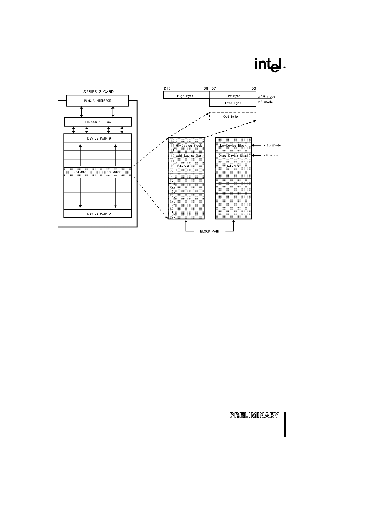
To support PCMCIA-compatible word-wide access,
devices are paired so that each accessible memory
block is 64 KWords (see Figure 2). Card logic allows
the system to write or read one word at a time, or
one byte at a time by referencing the high or low
byte. Erasure can be performed on the entire block
pair (high and low device blocks simultaneously), or
on the high or low byte portion separately.
Also in accordance with PCMCIA specifications this
product supports byte-wide operation, in which the
flash array is divided into 128K x 8 bit device blocks.
In this configuration, odd bytes are multiplexed onto
the low byte data bus.
5
SERIES 2 FLASH MEMORY CARDS
290434– 1
Figure 2. Memory Architecture. Each Device Pair Consists of Sixteen 64 KWord Blocks.
Series 2 Flash Memory Cards offer additional features over the Bulk Erase Flash Card product family
(refer to iMC001FLKA, iMC002FLKA and
iMC004FLKA data sheets). Some of the more notable enhancements include: high density capability,
erase blocking, internal write/erase automation,
erase suspension to read, Component Management
Registers that provide software control of devicelevel functions and a deep-sleep mode.
Erase blocking facilitates solid-state storage applications by allowing selective memory reclamation. Multiple 64 Kbyte blocks may be simultaneously erased
within the memory card as long as not more than
one block per device is erasing. This shortens the
total time required for erasure, but requires additional supply current. A block typically requires 1.6 seconds to erase. Each memory block can be erased
and completely written 100,000 times.
Erase suspend allows the system to temporarily interrupt a block erase operation. This mode permits
reads from alternate device blocks while that same
device contains an erasing block. Upon completion
of the read operation, erasure of the suspended
block must be resumed.
Write/erase automation simplifies the system software interface to the card. A two-step command sequence initiates write or erase operations and provides additional data security. Internal device circuits
automatically execute the algorithms and timings
necessary for data-write or block-erase operations,
including verifications for long-term data integrity.
While performing either data-write or block-erase,
the memory card interface reflects this by bringing
its RDY/BSY
Ý
(Ready/Busy) pin low. This output
goes high when the operation completes. This feature reduces CPU overhead and allows software
polling or hardware interrupt mechanisms. Writing
memory data is achieved in single byte or word increments, typically in 6 ms.
Read access time is 150 ns or less over the entire
operating temperature range.
The Reset-PowerDown mode reduces power consumption to less than 60 mA to help extend battery
life of portable host systems. Activated through software control, this mode optionally affects the entire
flash array (Global Reset-PowerDown Register) or
specific device pairs (Sleep Control Register).
6
SERIES 2 FLASH MEMORY CARDS
PCMCIA/JEIDA INTERFACE
The Series 2 Flash Memory Card interface supports
the PCMCIA 2.1 and JEIDA 4.1 68-pin card format
(see Tables 1 and 2). Detailed specifications are described in the PC Card Standard, Release 2.1, July,
1993, published by PCMCIA. The Series 2 Card conforms to the requirements of both Release 1 and
Release 2 of the PC Card Standard.
Series 2 Card pin definitions are equivalent to the
Bulk-Erase Flash Card except that certain No Connects are now used. A
22
through A24, RST (Reset),
and RDY/BSY
Ý
(Ready/Busy) have pin assign-
ments as set by the PCMCIA standard.
NOTE: The READY/BUSY signal is abbreviated as
RDY/BSY
Ý
by PCMCIA (card level) and as
RY/BY
Ý
by JEDEC (component level).
The outer shell of the Series 2 card meets all
PCMCIA/JEIDA Type 1 mechanical specifications.
See Figure 19 for mechanical dimensions.
WRITE PROTECT SWITCH
A mechanical write protect switch provides the
card’s memory array with internal write lockout. The
Write-Protect (WP) output pin reflects the status of
this mechanical switch. It outputs a high signal (V
OH
)
when writes are disabled. This switch does not lock
out writes to the Component Management Registers.
BATTERY VOLTAGE DETECT
PCMCIA requires two signals, BVD1and BVD2,be
supplied at the interface to reflect card battery condition. Flash Memory Cards do not require batteries.
When the power on reset cycle is complete, BVD
1
and BVD2are driven high to maintain compatibility.
CARD DETECT
Two signals, CD
1
Ý
and CD
2
Ý
, allow the host to determine proper socket seating. They reside at opposite ends of the connector and are tied to ground
within the memory card.
DESIGN CONSIDERATIONS
The Series 2 Card consists of two separate memory
planes: the Common Memory Plane (or Main Memory) and the Attribute Memory Plane. The Common
Memory Plane resides in the banks of device pairs
and represents the user-alterable memory space.
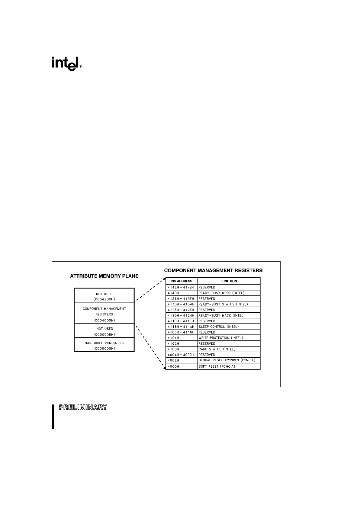
The Component Management Registers (CMR) and
the hardwired Card Information Structure (CIS) reside in the Attribute Memory Plane within the Card
Control Logic, as shown in Figure 3. The Card Control Logic interfaces the PCMCIA connector and the
internal flash memory array and performs address
decoding and data control.
Attribute Memory Plane
accessible with
REG (pin 61)
e
V
IL
290434– 2
INTEL
e
Performance Enhancement Register
PCMCIA
e
Defined in PCMCIA Release 2.0
Figure 3. Component Management Registers Allow S/W Control of Components within Card
7

SERIES 2 FLASH MEMORY CARDS
ADDRESS DECODE
Address decoding provides the decoding logic for
the 2 to 20 Device Chip Enables and the elements of
the Attribute Memory Plane. REG
Ý
selects between
the Common Memory Plane (REG
Ý
e
VIH) and the
Attribute Memory Plane (REG
Ý
e
VIL).
NOTE:
The Series 2 Card has
active
address inputs A0to
A
24
implying that reading and writing to addresses
beyond 32 Megabytes causes wraparound. Furthermore, reads to illegal addresses (for example, between 20 and 32 Meg on a 20 Megabyte card) returns Default data (00FFH or FFFFH).
The 28F008SA devices, storing data, applications or
firmware, form the Common Memory Plane accessed individually or as device pairs. Memory is linearly mapped in the Common Memory Plane. Three
memory access modes are available when accessing the Common Memory Plane: Byte-Wide, Word
Wide, and Odd-Byte modes.
Additional decoding selects the hardwired PCMCIA
CIS and Component Management Registers
mapped in the Attribute Memory Plane beginning at
address 000000H.
The 512 memory-mapped even-byte CMRs are linearly mapped beginning at address 4000H in the Attribute Memory Plane.
DATA CONTROL
Data Control Logic selects the path and direction for
accessing the Common or Attribute Memory Plane.
It controls any of the PCMCIA-defined Word-Wide,
Byte-Wide or Odd-Byte modes for either reads or
writes to these areas. As shown in Table 3, input
pins which determine these selections are REG
Ý
,
A
0
through A24,WEÝ,OEÝ,CE
1
Ý
, and CE
2
Ý
.
PCMCIA specifications allow only even-byte access
to the Attribute Memory Plane.
In Byte-Wide mode, bytes contiguous in software actually alternate between two device blocks of a device pair. Therefore, erasure of one device block
erases every other contiguous byte. In accordance
with the PCMCIA standard for memory configuration,
the Series 2 Card does not support confining contiguous bytes within one flash device when in by-8
mode.
8
SERIES 2 FLASH MEMORY CARDS
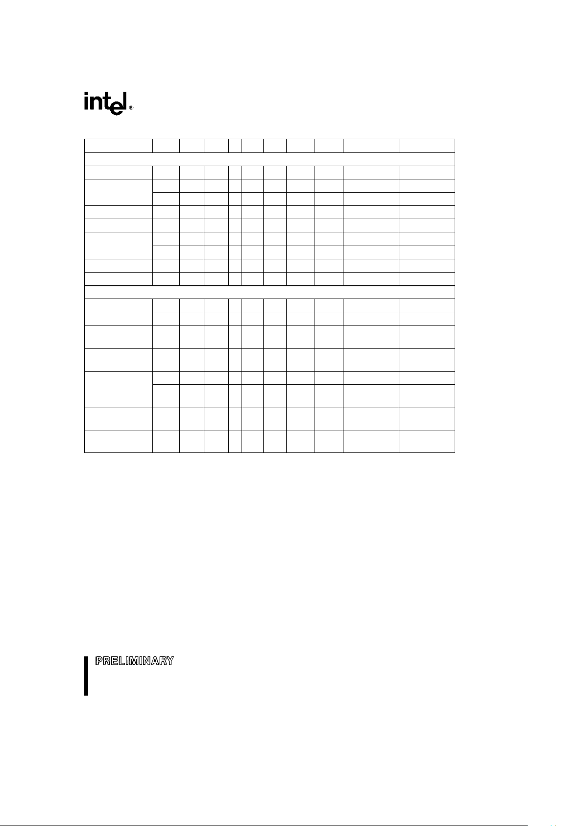
Table 3. Data Access Mode Truth Table
Function Mode REGÝCE
Ý
2
CE
Ý
1
A0OEÝWEÝV
PP2VPP1
D15–D
8
D7–D
0
COMMON MEMORY PLANE
STANDBY
(1)
XHHXXXV
PPL
(2)
V
PPL
(2)
HIGH-Z HIGH-Z
BYTE READ H H L L L H V
PPL
(2)
V
PPL
(2)
HIGH-Z EVEN-BYTE
HHLHLHV
PPL
(2)
V
PPL
(2)
HIGH-Z ODD-BYTE
WORD READ H L L X L H V
PPL
(2)
V
PPL
(2)
ODD-BYTE EVEN-BYTE
ODD-BYTE READ H L H X L H V
PPL
(2)
V
PPL
(2)
ODD-BYTE HIGH-Z
BYTE WRITE H H L L H L V
PPHVPPH
X EVEN-BYTE
HHLHHLV
PPHVPPH
X ODD-BYTE
WORD WRITE H L L X H L V
PPHVPPH
ODD-BYTE EVEN-BYTE
ODD-BYTE WRITE H L H X H L V
PPHVPPL
(2)
ODD-BYTE X
ATTRIBUTE MEMORY PLANE
BYTE READ L H L L L H X
(2)
X
(2)
HIGH-Z EVEN-BYTE
LHLHLHX
(2)
X
(2)
HIGH-Z INVALID
WORD READ L L L X L H X
(2)
X
(2)
INVALID EVEN-BYTE
DATA
(3)
ODD-BYTE READ L L H X L H X
(2)
X
(2)
INVALID HIGH-Z
DATA
(3)
BYTE WRITE L H L L H L X
(2)
X
(2)
X EVEN-BYTE
LHLHHLX
(2)
X
(2)
X INVALID
OPERATION
(3)
WORD WRITE L L L X H L X
(2)
X
(2)
INVALID EVEN-BYTE
OPERATION
(3)
ODD-BYTE WRITE L L H X H L X
(2)
X
(2)
INVALID X
OPERATION
(3)
NOTES:
1. Standby mode is valid in Common Memory or Attribute Memory access.
2. To meet the low power specifications, V
PP
e
V
PPL
; however V
PPH
presents no reliability problems.
3. Odd-Byte data are not valid during access to the Attribute Memory Plane.
4. H
e
VIH,LeVIL,XeDon’t Care.
9

SERIES 2 FLASH MEMORY CARDS
PRINCIPLES OF OPERATION
Intel’s Series 2 Flash Memory Card provides electrically-alterable, non-volatile, random-access storage.
Individual 28F008SA devices utilize a Command
User Interface (CUI) and Write State Machine
(WSM) to simplify block-erasure and data write operations.
COMMON MEMORY ARRAY
Figure 4 shows the Common Memory Plane’s organization. The first block pair (64 KWords) of Common Memory, referred to as the Common Memory
Card Information Structure Block,
optionally
extends
the hardwired CIS in the Attribute Memory Plane for
additional card information. This may be written during initial card formatting for OEM customization.
Since this CIS Block is part of Common Memory, its
data can be altered. Write access to the Common
Memory CIS Block is controlled by the Write Protect
Control Register which may be activated by system
software after power-up. Additionally, the entire
Common Memory plane (minus the Common Memory CIS Block) may be software write protected.
Note
that the Common Memory CIS Block is not part of
the Attribute Memory Plane. Do not assert REG
Ý
to
access the Common Memory CIS Block
.
13FFFFFH
Device Pair 9
1200000H
1000000H
Device Pair 8
0E00000H
Device Pair 7
0C00000H
Device Pair 6
0A00000H
Device Pair 5
0800000H
Device Pair 4
0600000H
Device Pair 3
0400000H
Device Pair 2
0200000H
Device Pair 1
0020000H
Device Pair 0
0000000H
Optional CIS
Figure 4. Common Memory Plane. Use
the Optional Common Memory Plane
CIS for Custom Card Format Information.
HARDWIRED CIS
The card’s structure description resides in the evenbyte locations starting at 0000H and going to the
CIS ending tuple (FNULL) within the Attribute Memory Plane. Data included in the hardwired CIS consists of tuples. Tuples are a variable-length list of
data blocks describing details such as manufacturer’s name, the size of each memory device and the
number of flash devices within the card.
COMPONENT MANAGEMENT
REGISTERS (CMRs)
The CMRs in the Attribute Memory Plane provide
special, software-controlled functionality. Card Control Logic includes circuitry to access the CMRs.
REG (PCMCIA, pin 61) selects the Attribute Memory
Plane (and therefore the CMRs) when equal to V
IL
.
CMRs are classified into two categories: those defined by PCMCIA R2.1 and those included by Intel
(referred to as Performance Enhancement Registers) to enhance the interface between the host system and the card’s flash memory array. CMRs (See
Figure 3) provide seven control functionsÐReadyBusy Interrupt Mode, Device Ready-Busy Status,
Device Ready-Busy Mask, Reset-PowerDown Control, Software-controlled Write Protection, Card
Status and Soft Reset.
SOFT RESET REGISTER (PCMCIA)
(CONFIGURATION OPTION)
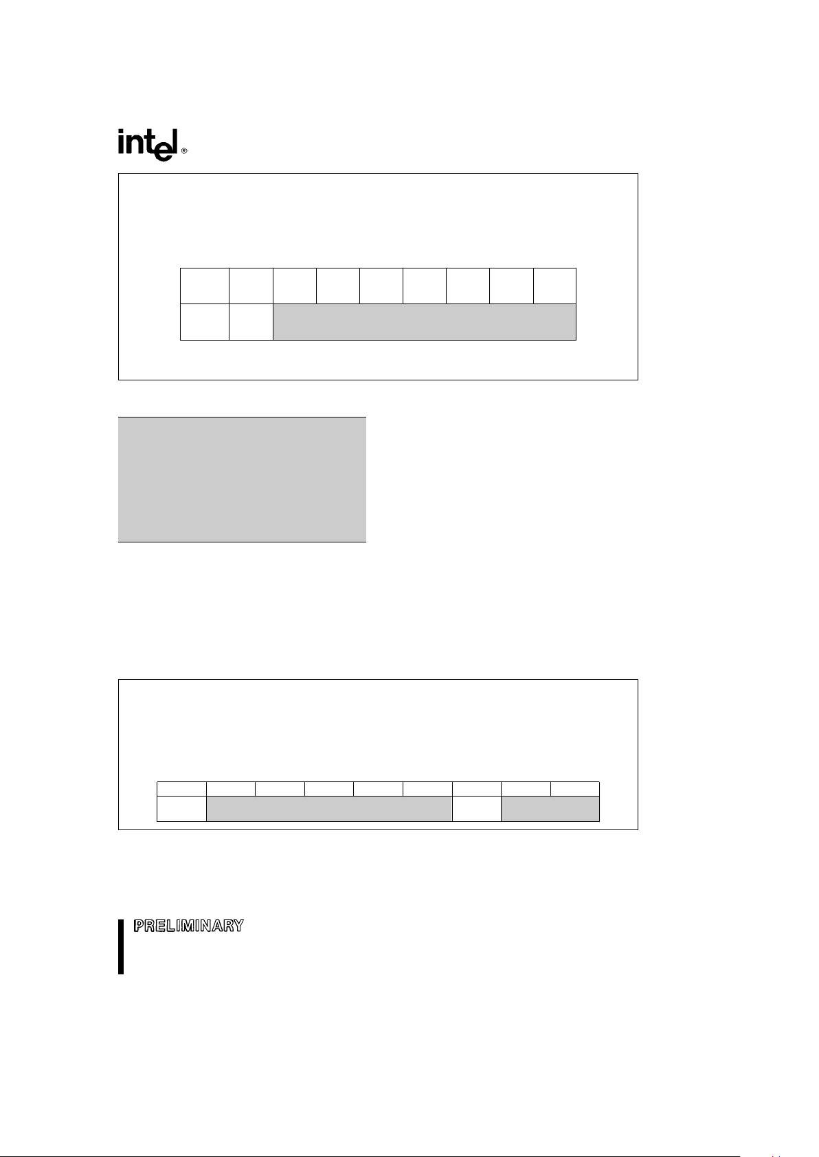
The SOFT RESET REGISTER (Attribute Memory
Plane Address 4000H, Figure 5) is defined in the
PCMCIA Release 2.0 specification as the Configuration Option Register.
Bit 7 is the soft reset bit (SRESET). Writing a 1 to
this bit initiates card reset to the power-on default
state (see Side Bar page 11). This bit must be
cleared to use the CMRs or to access the devices.
SRESET implements in software what the reset pin
implements in hardware. On power-up, the card automatically assumes default conditions. Similar to
the reset pin (pin 58), this bit clears at the end of a
power-on reset cycle or a system reset cycle.
Bits 0 through 6 are not used by this memory card,
but power up as zeroes for PCMCIA compatibility.
10
SERIES 2 FLASH MEMORY CARDS
SOFT RESET REGISTER
(CONFIGURATION OPTION REGISTER)
(Read/Write Register)
ADDRESS BIT 7 BIT 6 BIT 5 BIT 4 BIT 4 BIT 2 BIT 1 BIT 0
PCMCIA CONFIGURATION INDEX
4000H SRESET
RESETS TO ZERO ON POWER UP
1eRESET, CLEAR TO ACCESS CARD
Figure 5. SOFT RESET REGISTER (PCMCIA). Sets the Memory Card in the Power-On Default State.
POWER-ON DEFAULT CONDITIONS
#
All Devices Powered Up In Standby Mode
#
Common Memory Available For Writes
#
All Device Ready/Busy Outputs Unmasked
#
PCMCIA Ready/Busy Mode Enabled
#
Ready/Busy Output Goes To Ready
Global PowerDown Register (PCMCIA)
(Configuration and Status)
The Global Reset-PowerDown Register (Attribute
Memory Plane Address 4002H, Figure 6) is referred
to as the Configuration and Status Register in the
PCMCIA Release 2.0 specification.
Bit 2 (RP) controls global card power-down. Writing
a 1 to this bit places each device within the card into
‘‘Deep-Sleep’’ mode.
Devices in Deep-Sleep are not
accessible.
Recovery from power-down requires
500 ns for reads and 1 ms for writes.
The RP bit defaults to 0 on card power-up or reset.
Setting or clearing this bit has no affect on the bit
settings of the Sleep Control Register.
The remaining Global Reset-PwrDwn Register bits
are defined for Intel’s family of I/O cards and are
driven low for compatibility.
GLOBAL RESET-POWER-DOWN REGISTER
(CONFIGURATION AND STATUS REGISTER)
(Read/Write Register)
1ePOWER DOWN
ADDRESS BIT 7 BIT 6 BIT 5 BIT 4 BIT 3 BIT 2 BIT 1 BIT 0
4002H ZEROES RP ZEROES
Figure 6. GLOBAL RESET-PWRDWN REGISTER (PCMCIA). The RP
Bit Enables Reset PowerDown of All Flash Memory Devices.
11

SERIES 2 FLASH MEMORY CARDS
CARD STATUS REGISTER
(Read Only Register)
ADDRESS BIT 7 BIT 6 BIT 5 BIT 4 BIT 3 BIT 2 BIT 1 BIT 0
4100H ADM ADS SRESET CMWP RP CISWP WP RDY/BSY
Ý
Figure 7. CARD STATUS REGISTER (Intel) Provides a Quick Review of the Card’s Status
CARD STATUS REGISTER (INTEL)
The Read-Only, CARD STATUS REGISTER (Attribute Memory Plane Address 4100H, Figure 7) returns generalized status of the Series 2 Card and its
CMRs.
Bit 0 (RDY/BSY
Ý
) reflects the card’s RDY/BSY
Ý
(Ready-Busy) output. Software polling of this bit provides data-write or block-erase operation status. A
zero indicates a busy device(s) in the card.
Bit 1 (WP) reports the position of the card’s Write
Protection switch with 1 indicating write protected. It
reports the status of the WP pin.
Bit 2 (CISWP) reflects whether the Common Memory CIS is write protected using the WRITE PROTECT
REGISTER, with 1 indicating write protected.
Bit 3 (RP) reports whether the entire flash memory
array is in ‘‘Deep-Sleep’’ (Reset-PwrDwn) mode,
with 1 indicating ‘‘Deep-Sleep’’. This bit reflects the
RP bit of the GLOBAL RESET-POWERDOWN REGISTER. Powering down
all
device pairs individually
(using the Sleep Control Register), also sets this bit.
Bit 4 (CMWP) reports whether the Common Memory
Plane (minus Common Memory CIS) is write protected via the WRITE PROTECT REGISTER with 1 indicating write protected.
Bit 5 (SRESET) reflects the SRESET bit of the SOFT
RESET REGISTER. It reports that the card is in Soft
Reset with 1 indicating reset. When this bit is zero,
the flash memory array and CMRs may be accessed, otherwise clear it via the SRESET REGISTER.
Bit 6 (ADS, ANY DEVICE SLEEP) is the ‘‘ORed’’
value of the SLEEP CONTROL REGISTER. Powering down any device pair sets this bit.
Bit 7 (ADM, ANY DEVICE MASKED) is the ‘‘ORed’’
value of the READY/BUSY MASK REGISTER.
Masking any device sets this bit.
WRITE PROTECTION REGISTER
(INTEL)
The WRITE PROTECTION REGISTER (Attribute
Memory Plane Address 4104H, Figure 8) selects
whether the optional Common Memory CIS and the
remaining Common Memory blocks are write protected (see Figure 4).
Enable Common Memory CIS write protection by
writing a 1 to the CISWP Bit (bit 0).
Enable write protection of the remaining Common
Memory blocks by writinga1totheCMWP Bit (bit
1).
In the power-on default state, both bits are 0, and
therefore not write protected.
Reserved bits (2 – 7) have undefined values and
should be written as zeroes for future compatibility.
12
 Loading...