

Datasheet GT28F800F3T95, GT28F800F3T120, GT28F160F3T120, GT28F160F3B95, GT28F160F3B120 Datasheet (Intel Corporation)
...
E
PRODUCT PREVIEW
May 1998 Order Number: 290644-001
n
High Performance
54 MHz Effective Zero Wait-State
Performance
Synchronous Burst-Mode Reads
Asynchronous Page-Mode Reads
n
SmartVoltage Technology
2.7 V−3.6 V Read and Write
Operations for Low Power Designs
12 V VPP Fast Factory Programming
n
Flexible I/O Voltage
1.65 V I/O Reduces Overall System
Power Consumption
5 V-Safe I/O Enables Interfacing to
5 V Devices
n
Enhanced Data Protection
Absolute Write Protection with
V
PP
= GND
Block Locking
Block Erase/Program Lockout
during Power Transitions
n
Density Upgrade Path
8- and 16-Mbit
n
Manufactured on ETOX™ V Flash
Technology
n
Supports Code Plus Data Storage
Optimized for Flash Data Integrator
(FDI) Software
Fast Program Suspend Capability
Fast Erase Suspend Capability
n
Flexible Blocking Architecture
Eight 4-Kword Blocks for Data
32-Kword Main Blocks for Code
Top or Bottom Configurations
Available
n
Extended Cycling Capability
Minimum 10,000 Block Erase Cycles
Guaranteed
n
Low Power Consumption
Automatic Power Savings Mode
Decreases Power Consumption
n
Automated Program and Block Erase
Algorithms
Command User Interface for
Automation
Status Register for System
Feedback
n
Industry-Standard Packaging
56-Lead SSOP
µBGA* CSP
Intel’s Fast Boot Bloc k memory famil y renders high perf ormance as ynchronous page-m ode and sync hronous
burst reads making it an ideal memory solution for burs t CPUs. Combining high read performance wit h the
intrinsic non-volatility of flas h memory, this flash memory f amily eliminates the traditional redundant memory
paradigm of shadowing code from a slow nonvolatile storage source to a faster execution memory for
improved system performance. Therefore, it reduces the total memory requirement which helps increase
reliability and reduce overall system power consumption and cost.
This family of product s is manufac tured on Intel’ s 0.4 µm ETOX ™ V process technology . They are available
in industry-standard packages: the µBGA* CSP, ideal for board-constrained applications, and the rugged
56-lead SSOP.
FAST BOOT BLOCK
FLASH MEMORY FAMILY
8 AND 16 MBIT
28F800F3, 28F160F3
Includes Extended and Automotive Temperature Specifications

Information in this document is provided in connection with Intel products. No license, express or implied, by estoppel or
otherwise, to any intellectual property rights is granted by this document. Except as provi ded in Intel ’s Terms and Condi tions of
Sale for such products, Intel assumes no liability whatsoever, and Intel disclaims any express or implied warranty, relating to
sale and/or use of Intel products including liability or warranties relating to fitness for a particular purpose, merchantability, or
infringement of any patent, copyright or other intellectual property right. Intel products are not intended for use in medical, life
saving, or life sustaining applications.
Intel may make changes to specifications and product descriptions at any time, without notice.
The 28F800F3, 28F160F3 may contain design defects or errors known as errata which may cause the product to devi ate from
published specifications. Current characterized errata are available on request.
Contact your local Intel sales office or your distributor to obtain the latest specifications and before placing your product order.
Copies of documents which have an ordering number and are referenced in this document, or other Intel literature, may be
obtained from:
Intel Corporation
P.O. Box 5937
Denver, CO 80217-9808
or call 1-800-548-4725
or visit Intel’s Website at http://www.intel.com
COPYRIGHT © INTEL CORPORATION, 1998 CG-041493
*Third-party brands and names are the property of their respective owners

E FAST BOOT BLOCK DATASHEET
3
PRODUCT PREVIEW
CONTENTS
PAGE PAGE
1.0 INTRODUCTION .............................................5
1.2 Product Overview.........................................5
2.0 PRODUCT DESCRIPTION..............................6
2.1 Pinouts.........................................................6
2.2 Pin Description.............................................6
2.3 Memory Blocking Organization.....................9
2.3.1 Parameter Blocks..................................9
2.3.2 Main Blocks...........................................9
3.0 PRINCIPLES OF OPERATION .....................12
3.1 Bus Operations ..........................................12
3.1.1 Read....................................................12
3.1.2 Output Disable.....................................12
3.1.3 Standby...............................................12
3.1.4 Write....................................................12
3.1.5 Reset...................................................13
4.0 COMMAND DEFINITIONS............................13
4.1 Read Array Command................................15
4.2 Read Identifier Codes Command...............15
4.3 Read Status Register Command................15
4.4 Clear Status Register Command................15
4.5 Block Erase Command ..............................15
4.6 Program Command....................................17
4.7 Block Erase Suspend/Resume Command .17
4.8 Program Suspend/Resume Command.......17
4.9 Set Read Configuration Command.............19
4.9.1 Read Configuration..............................19
4.9.2 Frequency Configuration .....................20
4.9.3 Data Output Configuration...................20
4.9.4 WAIT# Configuration...........................20
4.9.5 Burst Sequence...................................20
4.9.6 Clock Configuration.............................20
4.9.7 Burst Length........................................20
5.0 DATA PROTECTION.....................................26
5.1 V
PP
= VIL for Complete Protection..............26
5.2 WP# = V
IL
for Block Locking ......................26
5.3 WP# = V
IH
for Block Unlocking...................26
6.0 V
PP
VOLTAGES............................................26
7.0 POWER CONSUMPTION..............................26
7.1 Active Power..............................................26
7.2 Automatic Power Savings ..........................26
7.3 Standby Power...........................................27
7.4 Power-Up/Down Operation.........................27
7.4.1 RST# Connection................................27
7.4.2 V
CC
, VPP and RST# Transitions...........27
7.5 Power Supply Decoupling ..........................27
7.5.1 V
PP
Trace on Printed Circuit Boards....27
8.0 ELECTRICAL SPECIFICATIONS .................28
8.1 Absolute Maximum Ratings........................28
8.2 Extended Temperature Operating
Conditions.................................................28
8.3 Capacitance...............................................29
8.4 DC Characteristics—Extended
Temperature..............................................30
8.5 AC Characteristics—Read-Only
Operations—Extended Temperature.........32
8.6 AC Characteristics—Write Operations—
Extended Temperature..............................38
8.7 AC Characteristics—Reset Operation—
Extended Temperature..............................40
8.8 Extended Temperature Block Erase and
Program Performance...............................41
8.9 Automotive Temperature Operating
Conditions.................................................41

FAST BOOT BLOCK DATASHEET E
4
PRODUCT PREVIEW
8.10 Capacitance.............................................42
8.11 DC Characteristics—Automotive
Temperature..............................................43
8.12 AC Characteristics—Read-Only
Operations—Automotive Temperature......44
8.13 Automotive Temperature Frequency
Configuration Settings...............................45
8.14 Automotive Temperature Block Erase and
Program Performance...............................45
9.0 ORDERING INFORMATION..........................46
10.0 ADDITIONAL INFORMATION.....................47
REVISION HISTORY
Date of
Revision
Version Description
05/12/98 -001 Original version

E FAST BOOT BLOCK DATASHEET
5
PRODUCT PREVIEW
1.0 INTRODUCTION
This datasheet contains 8- and 16-Mbit Fast Boot
Block memory informati on. Section 1.0 provides a
flash memory overview. Sections 2.0 through 8.0
describe the memory functionality and electrical
specifications for extended and automotive
temperature product offerings.
1.2 Product Overview
The Fast Boot Block flas h memory family provides
density upgrades with pinout compatibility for 8- and
16-Mbit densities. This family of products are high
performance, low voltage memories with a 16-bit
data bus and individually erasable blocks. These
blocks are optimally sized for code and data
storage. Eight 4-Kword parameter blocks are
positioned at either the top (denot ed by -T s uffix ) or
bottom (denoted by -B suffix) of the addres s map.
The rest of the device is grouped into
32-Kword main blocks. The upper two (or lower
two) parameter and all main blocks can be locked
for complete code protection.
The device’s optimized architecture and interface
dramatically increases read performance beyond
previously attainable levels. It supports
asynchronous page-mode and synchronous burst
reads from main blocks (parameter blocks support
single asynchronous and synchronous reads).
Upon initial power-up or return from reset, the
device defaults to a page-mode read conf iguration.
Page-mode read configuration is ideal for non-c lock
memory systems and is compatible with pagemode ROM. Synchronous burst reads are enabl ed
by writing to the read configuration register. In
synchronous burst mode, t he CLK input increm ents
an internal burst address generator, synchronizes
the flash memory with t he host CPU, and outputs
data on every rising (or falling) CLK edge up to
54 MHz (25 MHz for automotive temperature). An
output signal, WAIT#, is als o provided to eas e CPU
to flash memory communication and
synchronization during continuous burst operations.
In addition to the enhanced architecture and
interface, this family of products incorporates
SmartVoltage technology whi ch enables fast f actory
programming and low power designs. Specifically
designed for low voltage systems, Fast Boot Block
flash memory components support read operations
at 2.7 V (3.3 V for automoti ve temperature) V
CC
and
block erase and program operations at 2.7 V
(3.3 V for automotive temperature) and 12 V V
PP
.
The 12 V V
PP
option renders the fastest program
performance to increase factory programming
throughput. With the 2.7 V (3.3 V for automotive
temperature) V
PP
option, VCC and VPP can be tied
together for a simple, low power design. In addition
to the voltage flexibility, the dedicat ed V
PP
pin gives
complete data protection when V
PP
≤ V
PPLK
.
The flexible input/output (I/O) voltage capability
helps reduce system power consumption and
simplify interfacing to sub 2.7 V and 5 V CPUs.
Powered by V
CCQ
pins, the I/O buffers c an operate
at a lower voltage than the flash memory core. Wi th
V
CCQ
voltage at 1.65 V, the I/Os swing between
GND and 1.65 V, reducing I/O power cons umption
by 65% over standard 3 V flash memory
components. The low voltage and 5 V-safe feature
also helps ease CPU interfacing by adapting t o the
CPU’s bus voltage.
The device’s Command User Interface (CUI ) serv es
as the interface between t he system processor and
internal flash memory operation. A v alid command
sequence written to the CUI initiates device
automation. This automation is controlled by an
internal Write State Machine (WSM) which
automatically executes the algorithms and timings
necessary for block eras e and program operations.
The status register provides WSM feedback by
signifying block erase or program completion and
status.
Block erase and program automati on allows erase
and program operations to be executed using an
industry-standard two-write comm and sequence. A
block erase operation erases one bloc k at a time,
and data is programmed in word inc rements. Erase
suspend allows system software to suspend an
ongoing block erase operation in order to read from
or program data to any other block. Program
suspend allows system software to suspend an
ongoing program operation in order to read from
any other location.
Fast Boot Block flas h memory devi ces off er two low
power savings features: A utomatic Power Savings
(APS) and standby mode. The device automatically
enters APS mode following the completion of a read
cycle. Standby mode is initiated when the system
deselects the device by driving CE# inactive or
RST# active. RST# also res ets the device to read
array, provides write protection, and clears the
status register. Combined, these two features
significantly reduce power consumption.
FAST BOOT BLOCK DATASHEET E
6
PRODUCT PREVIEW
2.0 PRODUCT DESCRIPTION
This section describes the pinout and block
architecture of the device family.
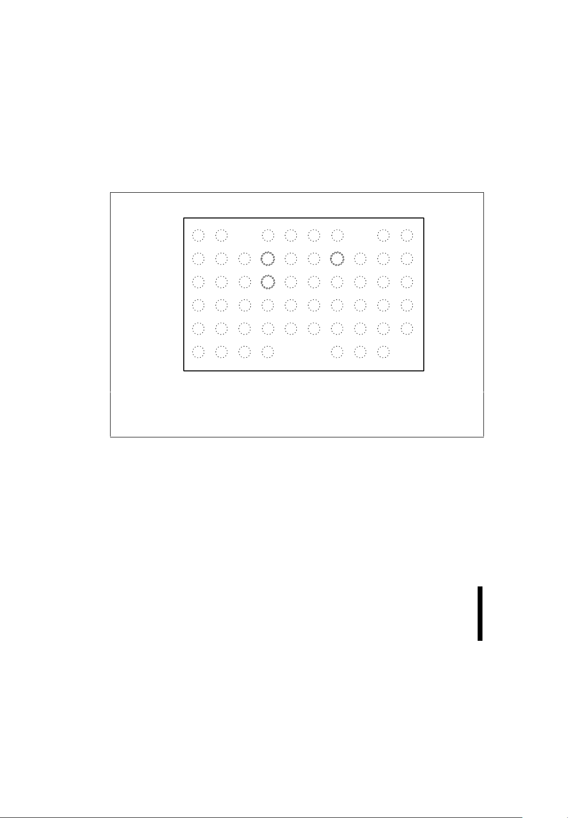
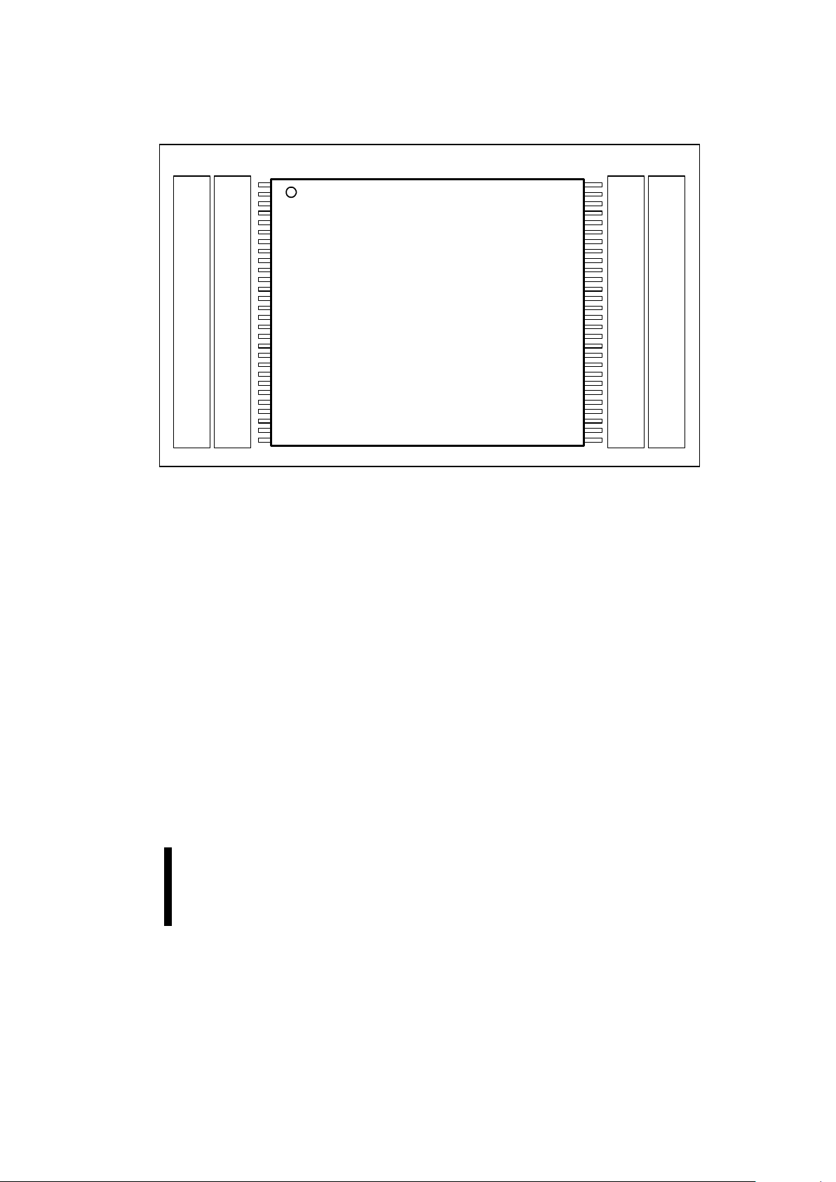
2.1 Pinouts
Intel’s Fast Boot Block flash memory family
provides upgrade paths in each pack age pinout up
to the 16-Mbit density. The family is available in
µBGA CSP and 56-lead SSOP pac kages. Pinouts
for the 8- and 16-Mbit components are illus trated in
Figures 1 and 2.
2.2 Pin Description
The pin description table describes pin usage.
123456789
A
B
C
D
E
F
10
A
14
A15A
12
A
11
A
8
GND
A
20
WE#
CLK V
CC
A
19
V
PP
A17A
5
A
4
A13A
10
A
21
A
18A7
A
6
A
1
A
2
A
3
A
9
WP#RST#
ADV#
V
CCQ
DQ
7
DQ
12
DQ10DQ9DQ0CE#DQ
13
DQ
11
DQ
4
A16DQ15DQ
6
DQ2DQ1OE#
WAIT# GND DQ14GND
V
CCQ
DQ8GND
A
0
DQ
5
DQ
3
V
CC
16M
32M
64M
NOTES:
1. Shaded connections indicate upgrade address connections. Lower density devices will not have upper address solder
balls. Routing is not recommended in this area.
2. A20 and A21 are the upgrade address for potential 32-Mbit and 64-Mbit devices (currently not on road map).
3. Reference the
Micro Ball Grid Array Package Mechanical Specification and Media Information
on Intel’s World Wide Web
home page for detailed package specifications.
Figure 1. 56-Ball µBGA* Package Pinout (Top View, Ball Down)
E FAST BOOT BLOCK DATASHEET
7
PRODUCT PREVIEW
16-Mbit
WE# WE#
RST# RST#
V
PP
V
PP
WP# WP#
NC A
19
A
1
A
1
A
2
A
2
A
3
A
3
A
4
A
4
A
5
A
5
A
6
A
6
A
7
A
7
A
17
A
17
A
18
A
18
DQ
9
DQ
9
DQ
1
DQ
1
DQ
8
DQ
8
DQ
0
DQ
0
OE# OE#
GND GND
CE# CE#
A
0
A
0
NC NC
V
CCQ
V
CCQ
DQ
2
DQ
2
DQ
10
DQ
10
DQ
3
DQ
3
DQ
11
DQ
11
V
CC
V
CC
CLKCLK
ADV#ADV#
GNDGND
NCNC
A
15
A
15
A
14
A
14
A
13
A
13
A
12
A
12
A
11
A
11
A
10
A
10
A
9
A
9
A
8
A
8
NCNC
GNDGND
DQ
6
DQ
6
DQ
14
DQ
14
DQ
7
DQ
7
DQ
15
DQ
15
GNDGND
V
CCQ
V
CCQ
A
16
A
16
WAIT#WAIT#
DQ
13
DQ
13
DQ
5
DQ
5
DQ
12
DQ
12
DQ
4
DQ
4
V
CC
V
CC
56-Lead SSOP
16 mm x 23.7 mm
TOP VIEW
1
2
3
4
5
6
7
8
9
10
11
12
13
14
15
16
17
18
19
20
21
22
23
24
25
26
27
28
56
55
54
53
52
51
50
49
48
47
46
45
44
43
42
41
40
39
38
37
36
35
34
33
32
31
30
29
8-Mbit 8-Mbit 16-Mbit
Figure 2. SSOP Pinout

FAST BOOT BLOCK DATASHEET E
8
PRODUCT PREVIEW
Table 1. Pin Descriptions
Sym Type Name and Function
A0–A
19
INPUT ADDRESS INPUTS: Inputs for addresses during read and write operations.
Addresses are internally latched during read and write cycles.
8-Mbit: A
0–18
, 16-Mbit: A
0–19
DQ0–
DQ
15
INPUT/
OUTPUT
DATA INPUT/OUTPUTS: Inputs data and commands during write cycles, outputs
data during memory array, status register (DQ
0
–DQ7), and identifier code read
cycles. Data pins float to high-impedance when the chip is deselected or outputs
are disabled. Data is internally latched during a write cycle.
CLK INPUT CLOCK: Synchronizes the flash memory to the system operating frequency during
synchronous burst-mode read operations. When configured for synchronous burstmode reads, address is latched on the first rising (or falling, depending upon the
read configuration register setting) CLK edge when ADV# is active or upon a rising
ADV# edge, whichever occurs first. CLK is ignored during asynchronous pagemode read and write operations.
ADV# INPUT ADDRESS VALID: Indicates that a valid address is present on the address inputs.
Addresses are latched on the rising edge of ADV# during read and write
operations. ADV# may be tied active during asynchronous read and write
operations.
CE# INPUT CHIP ENABLE: Activates the device’s control logic, input buffers, decoders, and
sense amplifiers. CE#-high deselects the device and reduces power consumption
to standby levels.
RST# INPUT RESET: When driven low, RST# inhibits write operations which provides data
protection during power transitions, and it resets internal automation. RST#-high
enables normal operation. Exit from reset sets the device to asynchronous read
array mode.
OE# INPUT OUTPUT ENABLE: Gates data outputs during a read cycle.
WE# INPUT WRITE ENABLE: Controls writes to the CUI and array. Addresses and data are
latched on the rising edge of the WE# pulse.
WP# INPUT WRITE PROTECTION: Provides a method for locking and unlocking all main
blocks and two parameter blocks.
When WP# is at logic low, lockable blocks are locked. If a program or erase
operation is attempted on a locked block, SR.1 and either SR.4 [program] or SR.5
[block erase] will be set to indicate the operation failed.
When WP# is at logic high, the lockable blocks are unlocked and can be
programmed or erased.
WAIT# OUTPUT WAIT: Provides data valid feedback when configured for synchronous burst-mode
and the burst length is set to continuous. This signal is gated by OE# and CE# and
is internally pull-up to V
CCQ
via a resistor. WAIT# from several components can be
tied together to form one system WAIT# signal.

E FAST BOOT BLOCK DATASHEET
9
PRODUCT PREVIEW
Table 1. Pin Descriptions
Sym Type Name and Function
V
PP
SUPPLY BLOCK ERASE AND PROGRAM POWER SUPPLY (2.7 V–3.6 V,
11.4 V–12.6 V): For erasing array blocks or programming data, a valid voltage
must be applied to this pin. With V
PP
≤ V
PPL
K
, memory contents cannot be altered.
Block erase and program with an invalid V
PP
voltage should not be attempted.
Applying 11.4 V–12.6 V to V
PP
can only be done for a maximum of 1000 cycles on
main blocks and 2500 cycles on the parameter blocks.
VPP
may be connected to
12 V for a total of 80 hours maximum (see Section 6.0 for details).
V
CC
SUPPLY DEVICE POWER SUPPLY (2.7 V–3.6 V): With VCC ≤ V
LKO
, all write attempts to
the flash memory are inhibited. Device operations at invalid V
CC
voltages should
not be attempted.
V
CCQ
SUPPLY OUTPUT POWER SUPPLY (1.65 V–2.5 V, 2.7 V–3.6 V): Enables all outputs to be
driven to 1.65 V to 2.5 V or 2.7 V to 3.6 V. When V
CCQ
equals 1.65 V–2.5 V, V
CC
voltage must not exceed 3.3 V and should be regulated to 2.7 V–2.85 V to achieve
lowest power operation (see
DC Characteristics
for detailed information).
This input may be tied directly to V
CC
.
GND SUPPLY GROUND: Do not float any ground pins.
NC NO CONNECT: Lead is not internally connected; it may be driven or floated.
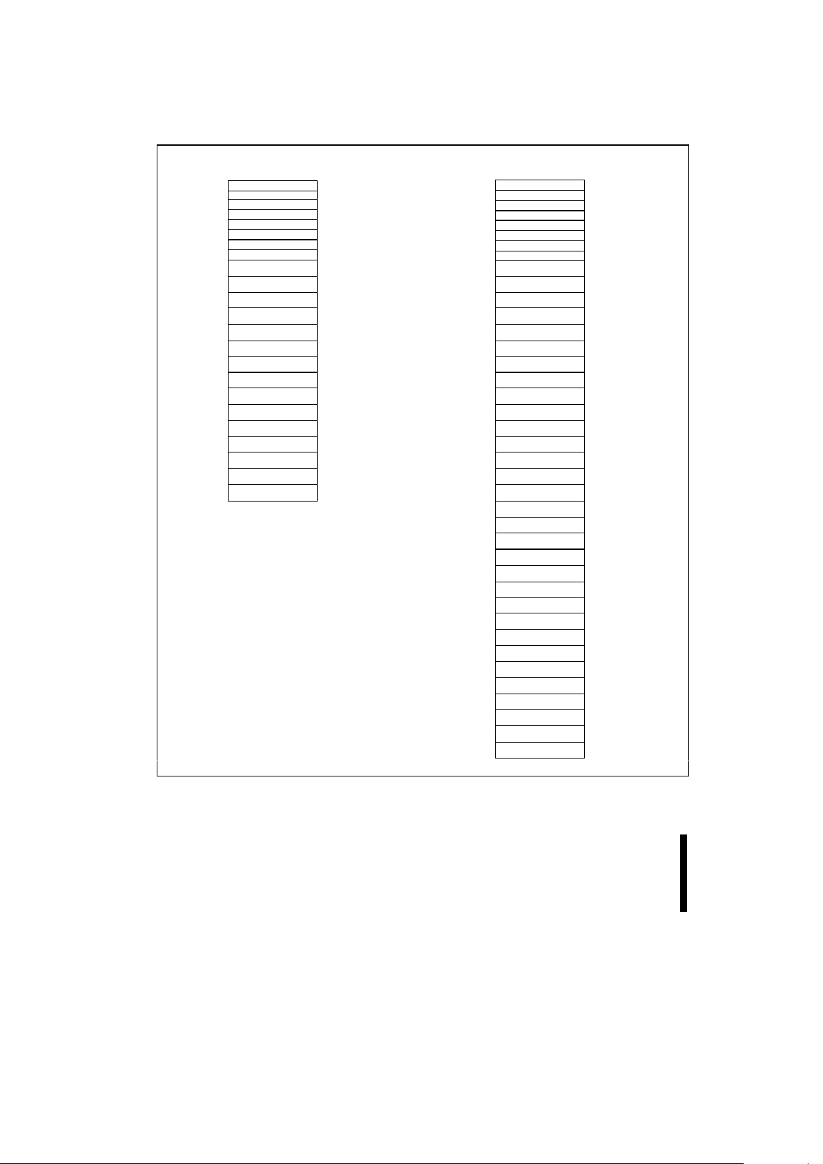
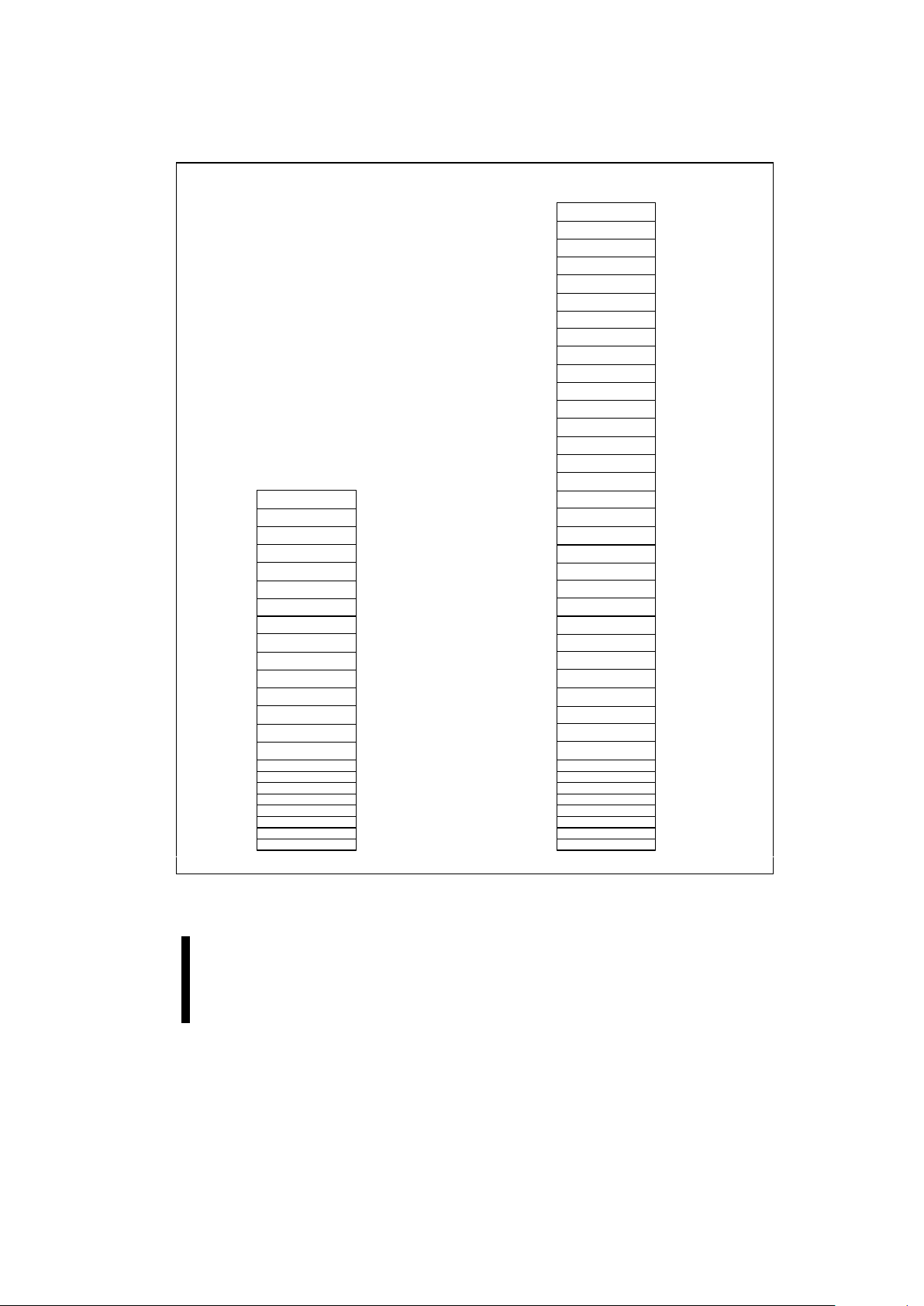
2.3 Memory Blocking Organization
The Fast Boot Block flash memory family is an
asymmetrically-blocked architecture that enables
system integration of code and data within a single
flash device. For the address locations of each
block, see the memory m aps in Figure 3 (top boot
blocking) and Figure 4 (bottom boot blocking).
2.3.1 PARAMETER BLOCKS
The Fast Boot Block flash memory architecture
includes parameter blocks to facilitate storage of
frequently updated small parameters that would
normally be stored in an EEPROM. By using
software techniques, the word-rewrite functionality
of EEPROMs can be emulated. Each 8- and
16-Mbit device contains eight 4-Kwords
(4,096-words) parameter blocks.
2.3.2 MAIN BLOCKS
After the parameter blocks, the remainder of the
array is divided into equal si ze m ain blocks for code
and/or data storage. The 8-Mbit device contains
fifteen 32-Kword (32,768-word) main blocks, and
the 16-Mbit device contains thirty-one 32-Kword
(32,768-word) main blocks.
FAST BOOT BLOCK DATASHEET E
10
PRODUCT PREVIEW
32-KWord
32-KWord
32-KWord
Address Range
78000h - 78FFFh
70000h - 77FFFh
68000h - 6FFFFh
60000h - 67FFFh
58000h - 5FFFFh
50000h - 57FFFh
48000h - 4FFFFh
40000h - 47FFFh
38000h - 3FFFFh
30000h - 37FFFh
28000h - 2FFFFh
20000h - 27FFFh
18000h - 1FFFFh
10000h - 17FFFh
08000h - 0FFFFh
00000h - 07FFFh
8-Mbit
32-KWord
32-KWord
32-KWord
32-KWord
32-KWord
32-KWord
32-KWord
32-KWord
32-KWord
32-KWord
32-KWord
32-KWord
Block 22
Block 21
Block 20
Block 19
Block 18
Block 17
Block 16
Block 15
Block 14
Block 13
Block 12
Block 11
Block 10
Block 9
Block 8
Block 7
Block 6
Block 5
Block 4
Block 3
Block 2
Block 1
Block 0
79000h - 79FFFh
7A000h - 7AFFFh
7B000h - 7BFFFh
7C000h - 7CFFFh
7D000h - 7DFFFh
7E000h - 7EFFFh
7F000h - 7FFFFh
4-KWord
4-KWord
4-KWord
4-KWord
4-KWord
4-KWord
4-KWord
4-KWord
32-KWord
32-KWord
32-KWord
Address Range
F8000h - F8FFFh
F0000h - F7FFFh
E8000h - EFFFFh
E0000h - E7FFFh
D8000h - DFFFFh
D0000h - D7FFFh
C8000h - CFFFFh
C0000h - C7FFFh
B8000h - BFFFFh
B0000h - B7FFFh
A8000h - AFFFFh
A0000h - A7FFFh
98000h - 9FFFFh
90000h - 97FFFh
88000h - 8FFFFh
80000h - 87FFFh
16-Mbit
32-KWord
32-KWord
32-KWord
32-KWord
32-KWord
32-KWord
32-KWord
32-KWord
32-KWord
32-KWord
32-KWord
32-KWord
Block 38
Block 37
Block 36
Block 35
Block 34
Block 33
Block 32
Block 31
Block 30
Block 29
Block 28
Block 27
Block 26
Block 25
Block 24
Block 23
Block 22
Block 21
Block 20
Block 19
Block 18
Block 17
Block 16
F9000h - F9FFFh
FA000h - FAFFFh
FB000h - FBFFFh
FC000h - FCFFFh
FD000h - FDFFFh
FE000h - FEFFFh
FF000h - FFFFFh
32-KWord
32-KWord 78000h - 7FFFFh
70000h - 77FFFh
68000h - 6FFFFh
60000h - 67FFFh
58000h - 5FFFFh
50000h - 57FFFh
48000h - 4FFFFh
40000h - 47FFFh
38000h - 3FFFFh
30000h - 37FFFh
28000h - 2FFFFh
20000h - 27FFFh
18000h - 1FFFFh
10000h - 17FFFh
32-KWord
32-KWord
32-KWord
32-KWord
32-KWord
32-KWord
32-KWord
32-KWord
32-KWord
32-KWord
32-KWord
32-KWord
Block 15
Block 14
Block 13
Block 12
Block 11
Block 10
Block 9
Block 8
Block 7
Block 6
Block 5
Block 4
Block 3
Block 2
08000h - 0FFFFh
00000h - 07FFFh
32-KWord
32-KWordBlock 1
Block 0
4-KWord
4-KWord
4-KWord
4-KWord
4-KWord
4-KWord
4-KWord
4-KWord
Figure 3. 8- and 16-Mbit Top Boot Memory Map
E FAST BOOT BLOCK DATASHEET
11
PRODUCT PREVIEW
Address Range
16-Mbit
32-KWord
32-KWord
32-KWord F8000h - FFFFFh
F0000h - F7FFFh
E8000h - EFFFFh
E0000h - E7FFFh
D8000h - DFFFFh
D0000h - D7FFFh
C8000h - CFFFFh
C0000h - C7FFFh
B8000h - BFFFFh
B0000h - B7FFFh
A8000h - AFFFFh
A0000h - A7FFFh
98000h - 9FFFFh
90000h - 97FFFh
88000h - 8FFFFh
32-KWord
32-KWord
32-KWord
32-KWord
32-KWord
32-KWord
32-KWord
32-KWord
32-KWord
32-KWord
32-KWord
32-KWord
Block 38
Block 37
Block 36
Block 35
Block 34
Block 33
Block 32
Block 31
Block 30
Block 29
Block 28
Block 27
Block 26
Block 25
Block 24
32-KWord
32-KWord 80000h - 87FFFh
78000h - 7FFFFh
70000h - 77FFFh
68000h - 6FFFFh
60000h - 67FFFh
58000h - 5FFFFh
50000h - 57FFFh
48000h - 4FFFFh
40000h - 47FFFh
38000h - 3FFFFh
30000h - 37FFFh
28000h - 2FFFFh
20000h - 27FFFh
18000h - 1FFFFh
32-KWord
32-KWord
32-KWord
32-KWord
32-KWord
32-KWord
32-KWord
32-KWord
32-KWord
32-KWord
32-KWord
32-KWord
Block 23
Block 22
Block 21
Block 20
Block 19
Block 18
Block 17
Block 16
Block 15
Block 14
Block 13
Block 12
Block 11
Block 10
10000h - 17FFFh
32-KWordBlock 9
00000h - 00FFFh
Block 7
Block 6
Block 5
Block 4
Block 3
Block 2
Block 1
Block 0
01000h - 01FFFh
02000h - 02FFFh
03000h - 03FFFh
04000h - 04FFFh
05000h - 05FFFh
06000h - 06FFFh
07000h - 07FFFh
4-KWord
4-KWord
4-KWord
4-KWord
4-KWord
4-KWord
4-KWord
4-KWord
32-KWordBlock 8 08000h - 0FFFFh
32-KWord
32-KWord
32-KWord
Address Range
78000h - 7FFFFh
70000h - 77FFFh
68000h - 6FFFFh
60000h - 67FFFh
58000h - 5FFFFh
50000h - 57FFFh
48000h - 4FFFFh
40000h - 47FFFh
38000h - 3FFFFh
30000h - 37FFFh
28000h - 2FFFFh
20000h - 27FFFh
18000h - 1FFFFh
10000h - 17FFFh
08000h - 0FFFFh
8-Mbit
32-KWord
32-KWord
32-KWord
32-KWord
32-KWord
32-KWord
32-KWord
32-KWord
32-KWord
32-KWord
32-KWord
32-KWord
Block 22
Block 21
Block 20
Block 19
Block 18
Block 17
Block 16
Block 15
Block 14
Block 13
Block 12
Block 11
Block 10
Block 9
Block 8
Block 7
Block 6
Block 5
Block 4
Block 3
Block 2
Block 1
Block 0 00000h - 00FFFh
01000h - 01FFFh
02000h - 02FFFh
03000h - 03FFFh
04000h - 04FFFh
05000h - 05FFFh
06000h - 06FFFh
4-KWord
4-KWord
4-KWord
4-KWord
4-KWord
4-KWord
4-KWord
4-KWord
07000h - 07FFFh
Figure 4. 8- and 16-Mbit Bottom Boot Memory Map

FAST BOOT BLOCK DATASHEET E
12
PRODUCT PREVIEW
3.0 PRINCIPLES OF OPERATION
The Fast Boot Block flash memory components
include an on-chip WSM to manage block erase
and program. It allows for CMOS-level control
inputs, fixed power suppli es, and minim al proces sor
overhead with RAM-like interface timings.
3.1 Bus Operations
All bus cycles to and from flash memory conform to
standard microprocessor bus cycles.
3.1.1 READ
The flash memory has three read modes av ailable:
read array, identifier codes, and status register.
These modes are accessible independent of the
V
PP
voltage. The appropriate read command (Read
Array, Read Identifier Codes, or Read Status
Register) must be written to the CUI to enter the
requested read mode. Upon initial power-up or exit
from reset, the device defaults to read array mode.
When reading information from main blocks in read
array mode, the device supports two highperformance read configurations: asynchronous
page-mode and synchronous burst-mode.
Asynchronous page-mode is t he default state and
provides high data transfer rate for non-clocked
memory subsystems. In this state, data is internally
read and stored in a high-speed page buffer. A
1:0
addresses data in the page buffer. The page size i s
four words. The other read configuration,
synchronous burst-mode, is enabled by writing to
read configuration register. This register sets the
read configuration, burst order, frequency
configuration, and burst length. In synchronous
burst-mode, the device latches the initial address
then outputs a sequence of data wi th res pect to t he
input CLK and read configuration setting.
Read operations from the parameter blocks,
identifier codes and status register transpire as
single asynchronous or synchronous read cycles.
The read configuration register setting determines
whether or not read operations are asynchronous or
synchronous.
For all read operations, CE# mus t be driven act ive
to enable the devices, ADV# must be driven low to
open the internal address latch, and OE# must be
driven low to activate t he outputs. In async hronous
mode, the address is latc hed when ADV# is driven
high. In synchronous mode, the address is latched
by ADV# going high or ADV# low in conjunction
with a rising (falling) clock edge, whichever occurs
first. WE# must be at V
IH
. Figures 14 through 19
illustrate different read cycles.
3.1.2 OUTPUT DISABLE
With OE# at a logic-high level (V
IH
), the device
outputs are disabled. Output pins DQ
0
–DQ15 are
placed in a high-impedance state.
3.1.3 STANDBY
Deselecting the device by bringi ng CE# to a logichigh level (V
IH
) places the device in standby mode,
which substantially reduces device power
consumption. In standby, outputs are placed in a
high-impedance state independent of OE#. If
deselected during program or erase operat ion, the
device continues to c onsume active power unt il the
program or erase operation is complete.
3.1.4 WRITE
Commands are written to the CUI using standard
microprocessor write timings when ADV#, WE#,
and CE# are active and OE# inactive. The CUI
does not occupy an addressable m emory location.
The address is latched on the ris ing edge of ADV#,
WE#, or CE# (whichever occurs first) and data
needed to execute a command is latched on the
rising edge of WE# or CE# (whichever goes high
first). Write operations are asynchronous.
Therefore, CLK is ignored during write operations.
Figure 20 illustrates a write operation.

E FAST BOOT BLOCK DATASHEET
13
PRODUCT PREVIEW
3.1.5 RESET
The device enters a reset mode when RST# is
driven low. In reset mode, i nternal c irc uitry is t urned
off and outputs are placed in a high-impedance
state.
After return from reset, a time t
PHQV
is required until
outputs are valid, and a delay (t
PHWL
or t
PHEL
) is
required before a write sequence can be init iated.
After this wake-up interval, normal operation is
restored. The device defaults to read array mode,
the status register is set to 80H, and the read
configuration register defaults to asynchronous
page-mode reads.
If RP# is taken low during a block erase or program
operation, the operation will be aborted and the
memory contents at the aborted location are no
longer valid. See Figure 21 for detail ed information
regarding reset timings.
4.0 COMMAND DEFINITIONS
Device operations are selected by writing specific
commands into the CUI. Table 3 defines these
commands.
Table 2. Bus Operations
Mode Notes RST# CE# ADV# OE# WE# Address V
PP
DQ
0–15
Reset V
IL
XXXXXXHigh Z
Standby V
IH
V
IH
XXXXXHigh Z
Output Disable V
IH
V
IL
XVIHV
IH
X X High Z
Read 1,2 V
IH
V
IL
V
IL
V
IL
V
IH
XXD
OUT
Read Identifier
Codes
V
IH
V
IL
V
IL
V
IL
V
IH
See
Table 4
X See
Table 4
Write 3,4 V
IH
V
IL
V
IL
V
IH
V
IL
XX D
IN
NOTES:
1. Refer to
DC Characteristics
. When VPP ≤ V
PPLK
, memory contents can be read, but not altered.
2. X can be V
IL
or VIH for control and address input pins and V
PPLK
or V
PPH1/2
for VPP. See
DC Characteristics
for V
PPLK
and
V
PPH1/2
voltages.
3. Command writes involving block erase or program are reliably executed when V
PP
= V
PPH1/2
and VCC = V
CC1/2
(see Section 8 for operating conditions at different temperatures).
4. Refer to Table 3 for valid D
IN
during a write operation.
FAST BOOT BLOCK DATASHEET E
14
PRODUCT PREVIEW
Table 3. Command Definitions
(1)
Bus Cycles First Bus Cycle Second Bus Cycle
Command Req’d. Notes Oper
(2)
Addr
(3)
Data
(4)
Oper
(2)
Addr
(3)
Data
(4)
Read Array/Reset 1 Write X FFH
Read Identifier Codes ≥ 2 5 Write X 90H Read IA ID
Read Status Register 2 Write X 70H Read X SRD
Clear Status Register 1 Write X 50H
Block Erase 2 6,7 Write X 20H Write BA D0H
Program 2 6,7,8 Write X 40H
or
10H
Write WA WD
Block Erase and Program
Suspend
1 6 Write X B0H
Block Erase and Program
Resume
1 6 Write X D0H
Set Read Configuration 2 Write X 60H Write RCD 03H
NOTES:
1. Commands other than those shown above are reserved by Intel for future device implementations and should not be used.
2. Bus operations are defined in Table 2.
3. X = Any valid address within the device.
IA = Identifier Code Address.
BA = Address within the block being erased.
WA = Address of memory location to be written.
RCD = Data to be written to the read configuration register. This data is presented to the device on A
15-0
; set all other
address inputs to “0.”
4. SRD = Data read from status register. See Table 5 for a description of the status register bits.
WD = Data to be written at location WA. Data is latched on the rising edge of WE# or CE# (whichever goes high first).
ID = Data read from identifier codes. See Table 4 for manufacturer and device codes.
RCD = Data to be written to read configuration register. See Table 6 for a description of the read configuration register bits.
5. Following the Read Identifier Codes command, read operations access manufacturer, device codes, and read
configuration register.
6. Following a block erase, program, and suspend operation, read operations access the status register.
7. To issue a block erase, program, or suspend operation to a lockable block, hold WP# at V
IH
.
8. Either 40H or 10H are recognized by the WSM as the program setup.

E FAST BOOT BLOCK DATASHEET
15
PRODUCT PREVIEW
4.1 Read Array Command
Upon initial device power-up or exit from reset, the
device defaults to read array mode. The read
configuration register defaults to asynchronous
page-mode. The Read Array command als o c auses
the device to enter read array mode. The device
remains enabled for reads until another c ommand
is written. Once the internal WSM has started a
block erase or program, the device will not
recognize the Read Array command until the WSM
completes its operation or unless the WSM is
suspended via an Erase or Program Suspend
command. The Read Array command functions
independently of the V
PP
voltage.
4.2 Read Identifier Codes
Command
The identifier code operation is initiat ed by writing
the Read Identifier Codes command. After writing
the command, read cycles retrieve the
manufacturer and device codes (see Table 4 for
identifier code values). Page-mode and burst reads
are not supported in this read mode. To t erminate
the operation, write another valid c omm and, li ke the
Read Array command. The Read Identifier Codes
command functions independently of the V
PP
voltage.
Table 4. Identifier Codes
Code
Address
(Hex)
Data
(Hex)
Manufacturer Code 00000 0089
Device Code 8 Mbit -T 00001 88F1
-B 00001 88F2
16 Mbit -T 00001 88F3
-B 00001 88F4
4.3 Read Status Register
Command
The status register can be read at any time by
writing the Read Status Register command to the
CUI. After writing this command, all subsequent
read operations output status register data until
another valid command is writ ten. Page-mode and
burst reads are not supported in this read mode.
The status register content i s updated and latched
on the rising edge of ADV# or rising (falling) CLK
edge when ADV# is low during synchronous burstmode or the falling edge of OE# or CE #, whichever
occurs first. The Read Status Register command
functions independently of the V
PP
voltage.
4.4 Clear Status Register
Command
Status register bits SR. 5, S R.4, S R.3, and SR. 1 are
set to “1”s by the WSM and can only be cleared by
issuing the Clear Status Regis ter command. These
bits indicate various error conditions. By allowing
system software to reset these bits, several
operations may be performed (such as cumul ati vely
erasing or writing several byt es in sequence). The
status register may be polled to determine if a
problem occurred during the sequence. The Clear
Status Register command functions independently
of the applied V
PP
voltage. After executing this
command, the device returns to read array mode.
4.5 Block Erase Command
Erase is executed one block at a time and init iated
by a two-cycle command. A block erase setup is
written first, followed by a block erase c onfirm. This
command sequence requires appropriate
sequencing and address within the block to be
erased (erase changes all block data to FFH).
Block preconditioning, eras e, and verify are handled
internally by the WSM. After the two-cycle block
erase sequence is written, the devic e automatically
outputs status register data when read (see
Figure 7,
Automated Block Erase Flowchart
). The
CPU can detect block erase completion by
analyzing status register bit SR.7.
When the block erase completes, check status
register bit SR.5 for an error fl ag (“1”). If an error i s
detected, check status register bits SR.4, SR.3, and
SR.1 to understand what caused t he failure. After
examining the status register, it should be c leared if
an error was detected before issuing a new
command. The device will remain in status regis ter
read mode until another command is written to the
CUI.

FAST BOOT BLOCK DATASHEET E
16
PRODUCT PREVIEW
Table 5. Status Register Definition
WSMS ESS ES PS VPPS PSS DPS R
76543210
NOTES:
SR.7 = WRITE STATE MACHINE STATUS (WSMS)
1 = Ready
0 = Busy
Check SR.7 to determine block erase or program
completion. SR.6
–0 are invalid while SR.7 =
“0.”
SR.6 = ERASE SUSPEND STATUS (ESS)
1 = Block Erase Suspended
0 = Block Erase in Progress/Completed
When an Erase Suspend command is issued, the
WSM halts execution and sets both SR.7 and SR.6
to
“1.” SR.6 remains set until an Erase Resume
command is written to the CUI.
SR.5 = ERASE STATUS (ES)
1 = Error in Block Erasure
0 = Successful Block Erase
If both SR.5 and SR.4 are “1”s after a block erase or
program attempt, an improper command sequence
was entered.
SR.4 = PROGRAM STATUS (PS)
1 = Error in Program
0 = Successful Program
SR.3 = VPP STATUS (VPPS)
1 = V
Low Detect, Operation Abort
0 = V
PP
OK
SR.3 does not provide a continuous V
PP
feedback.
The WSM interrogates and indicates the V
PP
level
only after a block erase or program operation. SR.3
is not guaranteed to reports accurate feedback
when V
PP
≠ V
PPH1/2
or V
PPLK
.
SR.2 = PROGRAM SUSPEND STATUS (PSS)
1 = Program Suspended
0 = Program in Progress/Completed
When an Program Suspend command is issued, the
WSM halts execution and sets both SR.7 and SR.2
to
“1.” SR.2 remains set until an Program Resume
command is written to the CUI.
SR.1 = DEVICE PROTECT STATUS (DPS)
1 = Block Erase or Program Attempted on a
Locked Block, Operation Abort
0 = Unlocked
If a block erase or program operation is attempted to
a locked block, SR.1 is set by the WSM and aborts
the operation if WP# = V
IL
.
SR.0 = RESERVED FOR FUTURE
ENHANCEMENTS (R)
SR.0 is reserved for future use and should be
masked out when polling the status register.

E FAST BOOT BLOCK DATASHEET
17
PRODUCT PREVIEW
4.6 Program Command
Program operation is executed by a two-cycle
command sequence. Program set up (standard 40H
or alternate 10H) is written, followed by a second
write that specifies the address and data. The WSM
then takes over, controlling the internal program
algorithm. After the program sequence is written,
the device automatically outputs status register
data when read (see Figure 8,
Automated Program
Flowchart
). The CPU can detect t he completion of
the program event by analyzing s tatus register bit
SR.7.
When the program operation completes, check
status register bit S R.4 for an error flag (“1”). If an
error is detected, check status register bits SR.5,
SR.3, and SR.1 to understand what caused the
problem. After examining the status register, it
should be cleared if an error was detect ed before
issuing a new command. The device will remain in
status register read mode unt il another com mand is
written to the CUI.
4.7 Block Erase Suspend/Resume
Command
The Block Erase Suspend command allows block
erase interruption to read or program data in
another blocks. Once the block erase process
starts, writing the B lock Erase Suspend command
requests that the WSM suspend the block erase
operation after a certain latency period. The device
continues to output st atus register data when read
after the Block Eras e Suspend command is is sued.
Status Register bits SR.7 and SR.6 indicate when
the block erase operation has been suspended
(both will be set to “1”). Specification t
WHRH2
defines
the block erase suspend latency.
At this point, a Read Array com mand c an be writ ten
to read data from blocks other than that which is
suspended. A Program command sequence can
also be issued during erase suspend to program
data in other blocks. Using the Program Suspend
command (see Section 4.8), a program operation
can be suspended during an erase suspend. The
only other valid commands while block erase is
suspended are Read Status Register and Block
Erase Resume.
During a block erase suspend, t he chip can go into
a pseudo-standby mode by taking CE# to V
IH
,
which reduces active current draw. V
PP
must
remain at V
PPH1/2
while block erase is sus pended.
WP# must also remain at V
IL
or VIH.
To resume the block erase operation, write the
Block Erase Resume command to the CUI. This will
automatically clear status register bits SR.6 and
SR.7. After the Erase Res ume com mand is written,
the device automatically outputs status register
data when read (see Figure 9,
Block Erase
Suspend/Resume Flowchart
). Block erase cannot
resume until program operations initiated during
block erase suspend have completed.
4.8 Program Suspend/Resume
Command
The Program Suspend command allows program
interruption to read data in other flash memory
locations. Once the program proc ess starts , writing
the Program Suspend command request s that the
WSM suspend the program operation aft er a certain
latency period. The device continues to output
status register data when read after issuing
Program Suspend command. Status register bits
SR.7 and SR.2 indicate when the block erase
operation has been suspended (both will be set t o
“1”). Specification t
WHRH1
defines the program
suspend latency.
At this point, a Read Array com mand c an be writ ten
to read data from blocks other than that which is
suspended. The only other valid commands while
block erase is suspended are Read S tatus Regist er
and Program Resume.
During a program suspend, the chip can go into a
pseudo-standby mode by taki ng CE# to V
IH
, which
reduces active current draw. V
PP
must remain at
V
PPH1/2
while program is suspended. WP# must
also remain at V
IL
or VIH.
To resume the program, write the P rogram Resume
command to the CUI. This will automatically clear
status register bits SR.7 and SR.2. After the Erase
Resume command is written, the device
automatically outputs status register data when
read (see Figure 10,
Program Suspend/Resume
Flowchart
).

FAST BOOT BLOCK DATASHEET E
18
PRODUCT PREVIEW
Table 6. Read Configuration Register Definition
RM R FC2 FC1 FC0 R DOC WC
15 14 13 12 11 10 9 8
BS CC R R R BL2 BL1 BL0
7654 3 210
NOTES:
RCR.15 = READ MODE (RM)
0 = Synchronous Burst Reads Enabled
1 = Page-Mode Reads Enabled (Default)
Read mode configuration effects reads from
main blocks. Parameter block, status register,
and identifier reads support single read cycles.
RCR.14 = RESERVED FOR FUTURE
ENHANCEMENTS (R)
These bits are reserved for future use. Set
these bits to
“0.”
RCR.13–11 = FREQUENCY CONFIGURATION (FC2-0)
001 = Code 1 reserved for future use
010 = Code 2
011 = Code 3
100 = Code 4
101 = Code 5
110 = Code 6
See Section 4.9.2 for information about the
frequency configuration and its effect on the
initial read.
Undocumented combinations of bits
RCR.14
–11 are reserved by Intel Corporation
for future implementations and should not be
used.
RCR.10 = RESERVED FOR FUTURE
ENHANCEMENTS (R)
These bits are reserved for future use. Set
these bits to
“0.”
RCR.9 = DATA OUTPUT CONFIGURATION (DOC)
0 = Hold Data for One Clock
1 = Hold Data for Two Clocks
Undocumented combinations of bits RCR.10–9
are reserved by Intel Corporation for future
implementations and should not be used.
RCR.8 = WAIT CONFIGURATION (WC)
0 = WAIT# Asserted During Delay
1 = WAIT# Asserted One Data Cycle Before Delay
RCR.7 = BURST SEQUENCE (BS)
0 = Intel Burst Order
1 = Linear Burst Order
RCR.6 = CLOCK CONFIGURATION (CC)
0 = Burst Starts and Data Output on Falling
Clock Edge
1 = Burst Starts and Data Output on Rising
Clock Edge
RCR.5–3 = RESERVED FOR FUTURE
ENHANCEMENTS (R)
These bits are reserved for future use. Set
these bits to
“0.”
RCR.2–0 = BURST LENGTH (BL2–0)
001 = 4 Word Burst
010 = 8 Word Burst
111 = Continuous Burst
In the asynchronous page mode, the burst
length always equals four words.
Undocumented combinations of bits RCR.2–0
are reserved by Intel Corporation for future
implementations and should not be used

E FAST BOOT BLOCK DATASHEET
19
PRODUCT PREVIEW
ADV# (V)
A
19-0
(A)
Valid
Address
CLK (C)
DQ
15-0
(D/Q)
Valid
Output
DQ
15-0
(D/Q)
Valid
Output
Valid
Output
Valid
Output
Valid
Output
DQ
15-0
(D/Q)
Valid
Output
Valid
Output
Valid
Output
Valid
Output
DQ
15-0
(D/Q)
Valid
Output
Valid
Output
DQ
15-0
(D/Q)
Valid
Output
Valid
Output
Valid
Output
Valid
Output
Code 2
Code 3
Code 4
Code 5
Code 6
Figure 5. Frequency Configuration
Table 7. Frequency Configuration Settings
(1)
Frequency Input CLK Frequency
Configuration Product = -90 Product = -120
Code VCC = 3.0 V-3.6 V VCC = 2.7 V-3.6 V VCC = 2.7 V-3.6 V
1 Reserved Reserved Reserved
2 ≤ 27 MHz ≤ 25 MHz ≤ 20 MHz
3 ≤ 40 MHz ≤ 33 MHz ≤ 28 MHz
4 ≤ 54 MHz ≤ 50 MHz ≤ 40 MHz
5 ≤ 66 MHz ≤ 60 MHz ≤ 50 MHz
6- ≤ 66 MHz ≤ 60 MHz
NOTES:
1. Reference Section 4.1.
Automotive Temperature Frequency Configuration Settings
for the corresponding frequency
configuration codes to different input CLK frequencies.
4.9 Set Read Configuration
Command
The Set Read Configuration command writes data
to the read configuration regist er. This operation is
initiated by a two-cycle command sequence. Read
configuration setup is wri tten, followed by a second
write that specifies the data to be writt en to the read
configuration register. This data is placed on the
address bus, A
15:0
, and is latched on the rising
edge of ADV#, CE#, or WE# (whichever occurs
first). The read configuration data sets the device’s
read configuration, burst order, frequency
configuration, and burst length. The command
functions independently of the applied V
PP
voltage.
After executing this comm and, the dev ice returns to
read array mode.
4.9.1 READ CONFIGURATION
The device supports two high performance read
configurations: asynchronous page-mode and

FAST BOOT BLOCK DATASHEET E
20
PRODUCT PREVIEW
synchronous burst-mode. Bit RCR.15 in the read
configuration register sets the read configuration.
Asynchronous page-mode is the default read
configuration state.
Parameter blocks, status register, and identifier
only support single asynchronous and synchronous
read operations.
4.9.2 FREQUENCY CONFIGURATION
The frequency configuration informs the device of
the number of clocks that must elapse after ADV#
is driven active before data will be available. This
value is determined by the input clock frequency.
See Table 7 for the specific input CLK frequency
configuration code
Figure 5 illustrates data output latency from ADV#
going active for different frequency configuration
codes.
4.9.3 DATA OUTPUT CONFIGURATION
The output configuration determines how many
clocks data will be held valid. The data hold time is
configurable as either one or two clocks.
The data output configuration must be set t o hold
data valid for two clock cycles when the frequency
configuration value 4 and burst length is greater
than four words. Otherwise, its setting will depend
on the system CPU’s data setup requirement.
DQ
15-0
(D/Q)
Valid
Output
DQ
15-0
(D/Q)
Valid
Output
Valid
Output
Valid
Output
CLK (C)
1 CLK
Data Hold
2 CLK
Data hold
Figure 6. Output Configuration
4.9.4 WAIT# CONFIGURATION
The WAIT# configuration bit controls the behavior
of the WAIT# output signal. This output signal can
be set to be asserted during or one CLK cycle
before an output delay when continuous burst
length is enabled. Its setting will depend on the
system and CPU characteristic.
4.9.5 BURST SEQUENCE
The burst sequence specifies the order in which
data is addressed in synchronous burst -mode. This
order is programmable as either linear or Intel burst
order. The continuous burst length only supports
linear burst order. The order chosen will depend on
the CPU characteristic. S ee Table 8 for m ore
details.
4.9.6 CLOCK CONFIGURATION
The clock configuration configures the device to
start a burst cycle, output data, and assert WAIT#
on the rising or falling edge of the clock. CLK
flexibility helps ease Fast Boot Block flash memory
interface to wide range of burst CPUs.
4.9.7 BURST LENGTH
The burst length is the number of words that the
device will output. The device supports burst
lengths of four and eight words. It also supports a
continuous burst mode. I n continuous burst mode,
the device will linearly output data until the internal
burst counter reaches the end of the device’s
burstable address space. Bit s RCR.2–0 in the read
configuration register set the burst length.
4.9.7.1 Continuous Burst Length
When operating in the continuous burst mode, t he
flash memory may incur an output delay when the
burst sequence crosses the first sixteen word
boundary. The starting address di ctates whether or
not a delay will occur. If the starting address is
aligned to a four word boundary, the delay will not
be seen. If the starti ng address is the end of a four
word boundary, the output delay will be equal t o t he
frequency configuration setting; this is the worst
case delay. The delay will only take place once
during a continuous burst acc ess, and if the burst
sequence never crosses a s ixteen word boundary,
the delay will never happen. Using the WAIT#
output pin in the continuous burs t configurat ion, the
system is informed if this output delay occurs.

E FAST BOOT BLOCK DATASHEET
21
PRODUCT PREVIEW
Table 8. Sequence and Burst Length
Burst Addressing Sequence (Dec)
Startin
g
Addr.
4 Word
Burst Length
8 Word
Burst Length
Continuous
Burst
(Dec) Linear Intel Linear Intel Linear
0 0-1-2-3 0-1-2-3 0-1-2-3-
4-5-6-7
0-1-2-3-
4-5-6-7
0-1-2-3-4-5-6-...
1 1-2-3-0 1-0-3-2 1-2-3-4-
5-6-7-0
1-0-3-2-
5-4-7-6
1-2-3-4-5-6-7-...
2 2-3-0-1 2-3-0-1 2-3-4-5-
6-7-0-1
2-3-0-1-
6-7-4-5
2-3-4-5-6-7-8-...
3 3-0-1-2 3-2-1-0 3-4-5-6-
7-0-1-2
3-2-1-0-
7-6-5-4
3-4-5-6-7-8-9-...
M M M MM M
6 6-7-0-1-
2-3-4-5
6-7-4-5-
2-3-0-1
6-7-8-9-10-11-12-...
7 7-0-1-2-
3-4-5-6
7-6-5-4-
3-2-1-0
7-8-9-10-11-12-13...
M
14 14-15-16-17-18-19-20-...
15 15-16-17-18-19-20-21-...
M

FAST BOOT BLOCK DATASHEET E
22
PRODUCT PREVIEW
Suspend
Blk. Erase
Loop
Start
Write 20H,
Block Address
Write D0H,
Block Address
Read Status Register
SR.7 =
Full Status
Check if Desired
Block Erase Complete
FULL STATUS CHECK PROCEDURE
Repeat for subsequent block erasures.
Full status check can be done after each block erase or after a
sequence of block erasures.
Write FFH after the last operation to place device in read array mode.
SR.5, SR.4, SR.3 and SR.1 are only cleared by the Clear Staus
Register command, in cases where multiple blocks are erased before
full status is checked.
If an error is detected, clear the status register before attempting retry
or other error recovery.
No
Yes
Suspend
Block Erase
1
0
Comments
Data = 20H
Addr = Within Block to Be
Erased
Data = D0H
Addr = Within Block to Be
Erased
Check SR.7
1 = WSM Ready
0 = WSM Busy
Comments
Check SR.3
1 = V
PP
Error Detect
Check SR.1
1 = Device Protect Detect
WP# = V
IL
Read Status Register
Data (See Above)
VPP Range Error
Device Protect Error
Block Erase
Successful
SR.3 =
SR.1 =
1
0
1
0
Command Sequence
Error
SR.4, 5 =
1
0
Block Erase ErrorSR.5 =
1
0
Status Register Data
Check SR.4, 5
Both 1 = Command Sequence
Error
Check SR.5
1 = Block Erase Error
Bus Operation
Write
Write
Standby
Read
Command
Erase Setup
Erase Confirm
Bus Operation
Standby
Standby
Standby
Standby
Command
Figure 7. Automated Block Erase Flowchart

E FAST BOOT BLOCK DATASHEET
23
PRODUCT PREVIEW
Suspend
Program
Loop
Start
Write 40H,
Address
Write Data and
Address
Read Status Register
SR.7 =
Full Status
Check if Desired
Program Complete
FULL STATUS CHECK PROCEDURE
Repeat for subsequent byte writes.
SR full status check can be done after each byte write or after a
sequence of program operations.
Write FFH after the last byte write operation to place device in read
array mode.
SR.4, SR.3 and SR.1 are only cleared by the Clear Staus Register
command, in cases where multiple locations are written before full
status is checked.
If an error is detected, clear the status register before attempting retry
or other error recovery.
No
Yes
Suspend
Program
1
0
Comments
Data = 40H
Addr = Location to Be
Written
Data = Data to Be Written
Addr = Location to Be
Written
Check SR.7
1 = WSM Ready
0 = WSM Busy
Comments
Check SR.3
1 = V
PP
Error Detect
Check SR.1
1 = Device Protect Detect
WP# = V
IL
Read Status Register
Data (See Above)
VPP Range Error
Device Protect Error
Program Successful
SR.3 =
SR.1 =
1
0
1
0
Program ErrorSR.4 =
1
0
Status Register Data
Check SR.4
1 = Data Write Error
Bus Operation
Write
Write
Standby
Read
Command
Program Setup
Data
Bus Operation
Standby
Standby
Standby
Command
Figure 8. Automated Program Flowchart

FAST BOOT BLOCK DATASHEET E
24
PRODUCT PREVIEW
Start
Write B0H
Read Status Register
Comments
Data = B0H
Addr = X
Data = D0H
Addr = X
SR.7 =
SR.6 =
Block Erase
Completed
Write FFH
Read Array Data
0
1
0
Status Register Data
Addr = X
Check SR.7
1 = WSM Ready
0 = WSM Busy
Check SR.6
1 = Block Erase Suspended
0 = Block Erase Completed
Read or Byte
Write?
Command
Erase Suspend
Erase Resume
Bus Operation
Write
Write
Read
Standby
Standby
Yes
Program
Program
Loop
Done
Write D0H
Block Erase Resumed
Read
Read Array
Data
No
1
Figure 9. Block Erase Suspend/Resume Flowchart

E FAST BOOT BLOCK DATASHEET
25
PRODUCT PREVIEW
Start
Write B0H
Read Status Register
No
Comments
Data = B0H
Addr = X
Data = FFH
Addr = X
SR.7 =
SR.2 =
1
Write FFH
Read Array Data
Program Completed
Done
Reading
Yes
Write FFHWrite D0H
Program Resumed Read Array Data
0
1
0
Read array locations from
block other than that being
written
Status Register Data
Addr = X
Check SR.7
1 = WSM Ready
0 = WSM Busy
Check SR.2
1 = Program Suspended
0 = Program Completed
Data = D0H
Addr = X
Bus Operation
Write
Write
Read
Read
Standby
Standby
Write
Command
Program
Suspend
Read Array
Program Resume
Figure 10. Program Suspend/Resume Flowchart

FAST BOOT BLOCK DATASHEET E
26
PRODUCT PREVIEW
5.0 DATA PROTECTION
The Fast Boot Block flash memory architecture
features hardware-lockable main blocks and two
parameter blocks, so critical code can be kept
secure while other parameter blocks are
programmed or erased as necessary.
5.1 VPP ≤ V
PPLK
for Complete
Protection
The VPP programming voltage can be held low for
complete write protection of all blocks in the flash
device. When V
PP
is below V
PPLK
, any block erase
or program operation will result in a error, prompting
the corresponding status register bit (SR.3) to be
set.
5.2 WP# = VIL for Block Locking
The lockable blocks are locked when WP# = VIL;
any block erase or program operation to a lock ed
block will result in an error, which will be reflected in
the status register. For top configuration, the top
two parameter and all main blocks (blocks #37,
#38, and #0 through 30 for the 16-M bit, blocks #21,
#22, and #0 through #14 for the 8-Mbit) are
lockable. For the bottom c onfiguration, the bottom
two parameter and all main blocks (blocks #0, #1,
and #8 through #38 for the 16-Mbit, blocks #0, #1,
and #8 through #22 for the 8-Mbit) are lockable.
Unlocked blocks can be programmed or erased
normally (unless V
PP
is below V
PPLK
).
5.3 WP# = VIH for Block Unlocking
WP# controls all block locking and VPP provides
protection against spurious writes. Table 9 defines
the write protection methods.
Table 9. Write Protection Truth Table
V
PP
WP# RST#
Write Protection
Provided
XXVILAll Blocks Locked
V
IL
XVIHAll Blocks Locked
≥ V
PPLK
V
IL
V
IH
Lockable
Blocks Locked
≥ V
PPLK
V
IH
V
IH
All
Blocks Unlocked
6.0 VPP VOLTAGES
Intel’s Fast Boot Block flash memory family
provides in-system programming and erase at
2.7 V–3.6 V (3.0 V–3.6 V for automotive
temperature) V
PP
. For customers requiring fast
programming in their manufacturing environment,
this family of products includes an additional lowcost, high-performance 12 V programming feature.
The 12 V V
PP
mode enhances programming
performance during short period of time typically
found in manufacturing processes; however, it is
not intended for extended use. 12 V may be applied
to V
PP
during block erase and program operations
for a maximum of 1000 cycles on the main blocks
and 2500 cycles on the parameter blocks. V
PP
may
be connected to 12 V for a total of 80 hours
maximum. Stress ing the devi ce bey ond thes e lim its
may cause permanent damage.
7.0 POWER CONSUMPTION
While in operation, the flash device consumes
active power. However, Intel Flash devices have
power savings that can s ignificantly reduce ov erall
system power consumption. The Automatic Power
Savings (APS) feature reduces power consumption
when the device is idle. I f CE# is deasserted, the
flash enters its standby mode, where current
consumption is even lower. The combination of
these features minimizes overall memory power
and system power consumption.
7.1 Active Power
With CE# at a logic-low level and RST# at a logichigh level, the device is in active mode. Active
power is the largest contributor to overall system
power consumption. Minimi zing active current has a
profound effect on system power consumption,
especially for battery-operated devices.
7.2 Automatic Power Savings
Automatic Power Savings (APS) provides lowpower operation during active mode, allowing the
flash to put itself into a low current state when not
being accessed. Aft er data is read from the memory
array, the device’s power consumption enters the
APS mode where typical I
CC
current is comparable
to I
CCS
. The flash stays in this static state with
outputs valid until a new location is read.

E FAST BOOT BLOCK DATASHEET
27
PRODUCT PREVIEW
7.3 Standby Power
With CE# at a logic-high level (VIH) and the CUI in
read mode, the flash memory is in standby mode,
which disables much of the device’s circuitry and
substantially reduces power consumption. Outputs
(DQ
0
–DQ15) are placed in a high-impedance st ate
independent of the status of the OE# signal. I f CE#
transitions to a logic-high level during erase or
program operations, the device will continue to
perform the operation and consume corresponding
active power until the operation is completed.
System engineers should anal yz e the breakdown of
standby time versus active time and quantify the
respective power consumption in each mode for
their specific application. This will provide a more
accurate measure of applicat ion-specif ic power and
energy requirements.
7.4 Power-Up/Down Operation
The device is protected against accidental block
erasure or programming during power transitions.
Power supply sequencing is not required, since the
device is indifferent as to which power supply , V
PP
,
V
CC
, or V
CCQ
, powers-up first.
7.4.1 RST# CONNECTION
The use of RST# during system reset is important
with automated program/erase devices since the
system expects to read from the flash memory
when it comes out of res et. If a CPU reset occ urs
without a flash memory reset, proper CPU
initialization will not occur because the flash
memory may be providing status information
instead of array data. Int el recommends c onnecting
RST# to the system reset signal to allow proper
CPU/flash initialization following system reset.
System designers must guard against spurious
writes when V
CC
voltages are above V
LKO
and V
PP
is active. Since both WE# and CE# mus t be low for
a command write, driving either signal to V
IH
will
inhibit writes to the device. The CUI architecture
provides additional protection since alteration of
memory contents can only occur after successful
completion of the two-step command sequences.
The device is also disabled unti l RST# is brought to
V
IH
, regardless of the stat e of its c ontrol inputs. By
holding the device in reset during power-up/down,
invalid bus conditions during power-up can be
masked, providing yet another level of memory
protection.
7.4.2 V
CC
, VPP AND RST# TRANSITIONS
The CUI latches commands as issued by system
software and is not altered by V
PP
or CE#
transitions or WSM actions. Its default state upon
power-up, after exit from deep power-down mode or
after V
CC
transitions above V
LKO
(Lockout voltage),
is read array mode.
After any block erase or program operation is
complete (even after V
PP
transitions down to
V
PPLK
), the CUI must be reset t o read array mode
via the Read Array command if access to the fl ash
memory array is desired.
7.5 Power Supply Decoupling
Flash memory’s power switching characteristics
require careful device decoupling. System
designers should consider three supply current
issues:
1. Standby current levels (I
CCS
)
2. Active current levels (I
CCR
)
3. Transient peaks produced by falling and rising
edges of CE#.
Transient current magnitudes depend on t he devi ce
outputs’ capacitiv e and inductive loading. Two-line
control and proper decoupling capacitor selection
will suppress these transient voltage peaks. Each
flash device should have a 0.1 µF ceramic
capacitor connected between eac h V
CC
and GND,
and between its V
PP
and GND. These highfrequency, inherently low-inductance capacitors
should be placed as close as possible to the
package leads.
7.5.1 V
PP
TRACE ON PRINTED CIRCUIT
BOARDS
Designing for in-system writes to the flash memory
requires special consideration of the V
PP
power
supply trace by the printed c ircuit board designer.
The V
PP
pin supplies the flash mem ory cel ls c urrent
for programming and erasing. V
PP
trace widths and
layout should be similar to that of V
CC
. Adequate
V
PP
supply traces, and decoupling capacitors
placed adjacent to the component, will decrease
spikes and overshoots.

FAST BOOT BLOCK DATASHEET E
28
PRODUCT PREVIEW
8.0 ELECTRICAL SPECIFICATIONS
8.1 Absolute Maximum Ratings*
Temperature under Bias............ –40 °C to +125 °C
Storage Temperature................. –65 °C to +125 °C
Voltage On Any Pin
(except V
CC
, V
CCQ
, and VPP)–0.5 V to +5.5 V
(1)
VPP Voltage .........................–0.5 V to +13.5 V
(1,2,4)
VCC and V
CCQ
Voltage............... –0.2 V to +5.0 V
(1)
Output Short Circuit Current.....................100 mA
(3)
NOTICE: This datasheet contains preliminary
information on products in the design phase of
development.
The specifications are subject to
change without notice.
Verify with your local Intel
Sales office that you have the latest datasheet
before finalizing a design.
*WARNING: Stressing the device beyond the
“Absolute Maximum Rat i ngs ” may cause permanent
damage. These are stress ratings only. Operation
beyond the “Operating Conditions” is not
recommended and extended exposure beyond the
“Operating Conditions” may affect device reliability.
NOTES:
1. All specified voltages are with respect to GND. Minimum DC voltage is –0.5 V on input/output pins and –0.2 V on V
CC
and
V
PP
pins. During transitions, this level may undershoot to –2.0 V for periods <20 ns. Maximum DC voltage on input/output
pins and V
CC
is VCC +0.5 V which, during transitions, may overshoot to VCC +2.0 V for periods <20 ns.
2. Maximum DC voltage on V
PP
may overshoot to +14.0 V for periods <20 ns.
3. Output shorted for no more than one second. No more than one output shorted at a time.
4. V
PP
Program voltage is normally 2.7 V–3.6 V. Connection to supply of 11.4 V–12.6 V can only be done for 1000 cycles on
the main blocks and 2500 cycles on the parameter blocks during program/erase. V
PP
may be connected to 12 V for a total
of 80 hours maximum.
8.2 Extended Temperature Operating Conditions
Symbol Parameter Notes Min Max Unit
T
A
Operating Temperature –40 +85 °C
V
CC1
VCC Supply Voltage 1 2.7 2.85 V
V
CC2
VCC Supply Voltage 1 2.7 3.3 V
V
CC3
VCC Supply Voltage 1,4 2.7 3.6 V
V
CCQ1
I/O Voltage 1,2 1.65 2.5 V
V
CCQ2
I/O Voltage 1,2 1.8 2.5 V
V
CCQ3
I/O Voltage 1,2,4 2.7 3.6 V
V
PPH1
VPP Supply Voltage 1 2.7 3.6 V
V
PPH2
VPP Supply Voltage 1,4 11.4 12.6 V
Cycling Block Erase Cycling 3 10,000 Cycles
NOTES:
1. See
DC Characteristics
tables for voltage range-specific specifications.
2. The voltage swing on the inputs, V
IN
is required to match V
CCQ
.
3. Applying V
PP
= 11.4 V–12.6 V during a program or erase can only be done for a maximum of 1000 cycles on the main
blocks and 2500 cycles on the parameter blocks. A hard connection to V
PP
= 11.4 V–12.6 V is not allowed and can cause
damage to the device.
4. V
CC
, V
CCQ
, and V
PP1
must share the same supply when all three are between 2.7 V and 3.6 V.

E FAST BOOT BLOCK DATASHEET
29
PRODUCT PREVIEW
8.3 Capacitance
(1)
T
A
= +25 °C, f = 1 MHz
Sym Parameter Typ Max Unit Condition
C
IN
Input Capacitance 6 8 pF VIN = 0.0 V
C
OUT
Output Capacitance 8 12 pF V
OUT
= 0.0 V
NOTE:
1. Sampled, not 100% tested.
V
CCQ
0V
V
CCQ
/2 V
CCQ
/2
T
est P
o
in
ts
Input Output
AC test inputs are driven at V
CCQ
min. for a Logic "1" and 0.0 V for a Logic "0." Input timing begins, and output timing ends, at
V
CCQ
/2. Input rise and fall times (10% to 90%) < 5 ns. Worst case speed conditions are when V
CCQ
= 2.7 V.
Figure 11. Transient Input/Output Reference Waveform for VCC = 2.7 V−3.6 V
Device
Under Test
V
CCQ
CLR
2
R
1
Out
NOTE:
See table for component values.
Figure 12. Transient Equivalent Testing
Load Circuit
Test Configuration Component Value
for Worst Case Speed Conditions
Test Configuration CL (pF) R1 (Ω)R2 (Ω)
2.7 V Standard Test 50 25K 25K
1.65 V Standard Test 50 16.7K 16.7K
NOTE:
C
L
includes jig capacitance.

FAST BOOT BLOCK DATASHEET E
30
PRODUCT PREVIEW
8.4 DC Characteristics—Extended Temperature
(1)
V
CC
2.7 V–3.6 V 2.7 V–2.85 V 2.7 V–3.3 V
V
CCQ
2.7 V–3.6 V 1.65 V–2.5 V 1.65 V–2.5 V
Sym Parameter Note Typ Max Typ Max Typ Max Unit Test Conditions
I
LI
Input Load
Current
6 ± 1 ± 1 ± 1 µA VCC = VCCMax
V
CCQ
= V
CCQ
Max
V
IN
= V
CCQ
or GND
I
LO
Output Leakage
Current
6 ± 10 ± 10 ± 10 µA VCC = VCCMax
V
CCQ
= V
CCQ
Max
Output Leakage
Current for
WAIT#
± 25 ± 25 ± 25
V
IN
= V
CCQ
or GND
I
CCSVCC
Standby
Current
6 30 50 20 50 150 250 µA VCC = VCCMax
CE# = RP# = V
CC
or during Program/
Erase Suspend
I
CCRVCC
Read
Current
4,6 45 60 30 45 40 55 mA
Asynchronous
t
AVAV
= Min
V
IN
= VIH or V
IL
45 60 30 45 40 55 mA
Synchronous
CLK = 33 MHz
CE# = V
IL
OE# = V
IH
Burst length = 1
I
CCWVCC
Program
Current
3,6 8 20 8 20 8 20 mA VPP = V
PP1, 2
Program in Progress
I
CCE
V
Erase
Current
3,6 8 20 8 20 8 20 mA V
PP
= V
PP1, 2
Erase in Progress
I
PPR
V
Read
Current
2 ±15 2 ±15 2 ±15 µA V
PP
≤ V
CC
3 50 200 50 200 50 200 µA V
PP
> V
CC
I
PPW
VPP Program
Current
3103510351035mAV
PP
=V
PP1
Program in Progress
210210210mAV
PP
= V
PP2
Program in Progress
I
PPEVPP
Erase
Current
3122513251325mAVPP = V
PP1
Program in Progress
825825825mAV
PP
= V
PP2
Program in Progress
I
PPES
I
PPWS
V
Erase
Suspend Current
3 50 200 50 200 50 200 µA VPP = V
PP1, 2
Program or Erase
Suspend in Progress

E FAST BOOT BLOCK DATASHEET
31
PRODUCT PREVIEW
8.4 DC Characteristics—Extended Temperature (Continued)
V
CC
2.7 V–3.6 V 2.7 V–2.85 V 2.7 V–3.3 V
V
CCQ
2.7 V–3.6 V 1.65 V–2.5 V 1.8 V–2.5 V
Sym Parameter Note Min Max Min Max Min Max Unit Test Conditions
V
IL
Input Low
Voltage
–0.4 0.4 –0.2 0.2 –0.2 0.2 V
V
IH
Input High
Voltage
V
CCQ
–
0.4V
V
CCQ
–
0.2V
V
CCQ
–
0.2V
V
V
OL
Output Low
Voltage
0.10 -0.10 0.10 -0.10 0.10 V VCC = VCCMin
V
CCQ
= V
CCQ
Min
I
OL
= 100 µA
V
OH
Output High
Voltage
V
CCQ
–
0.1V
V
CCQ
–
0.1V
V
CCQ
–
0.1V
VV
CC
= VCCMin
V
CCQ
= V
CCQ
Min
I
OH
= –100 µA
V
PPLK
V
Lock-Out
Voltage
2 1.5 1.5 1.5 1.5 V Complete Write
Protection
V
PP1VPP
during 2 2.7 3.6 V
V
PP2
Program and 2 2.7 2.85 V
V
PP3
Erase Operations 2 2.7 3.3 V
V
PP4
2,5 11.4 12.6 11.4 12.6 11.4 12.6 V
V
LKOVCC
Prog/Erase
Lock Voltage
1.5 1.5 1.5 V
V
LKO2VCCQ
Prog/Erase
Lock Voltage
1.2 1.2 1.2 V
NOTES:
1. All currents are in RMS unless otherwise noted. Typical values at normal V
CC
, T = +25 °C.
2. I
CCES
is specified with device deselected. If device is read while in erase suspend, current draw is sum of I
CCES
and I
CCR
.
3. Erases and program operations are inhibited when V
PP
≤ V
PPLK
, and not guaranteed outside the valid VPP ranges of V
PPH1
and V
PPH2
.
4. Sampled, not 100% tested.
5. Automatic Power Savings (APS) reduces I
CCR
to approximately standby levels, in static operation.
6. Applying V
PP
= 11.4 V–12.6 V during program/erase can only be done for a maximum of 1000 cycles on the main blocks
and 2500 cycles on the parameter blocks. V
PP
may be connected to 12 V for a total of 80 hours maximum.
7. The specification is the sum of V
CC
and V
CCQ
currents.

FAST BOOT BLOCK DATASHEET E
32
PRODUCT PREVIEW
8.5 AC Characteristics—Read-Only Operations
(1,6)
—
Extended Temperature
Product –95 –120
V
CC
3.0 V–3.6 V 2.7 V–3.6 V 2.7 V–3.6 V
# Sym Parameter Notes Min Max Min Max Min Max Unit
R1 t
CLK
CLK Period 15 15 15 ns
R2 tCH(tCL) CLK High (Low) Time 2.5 2.5 2.5 ns
R3 t
CHCL
CLK Fall (Rise) Time 5 5 5 ns
R4 t
AVCH
Address Valid Setup to CLK 7 7 7 ns
R5 t
VLCH
ADV# Low Setup to CLK 7 7 7 ns
R6 t
ELCH
CE# Low Setup to CLK 7 7 7 ns
R7 t
CHQV
CLK to Output Delay 14 16 23 ns
R8 t
CHQX
Output Hold from CLK 5 5 5 ns
R9 t
CHAX
Address Hold from CLK 3 10 10 10 ns
R10 t
CHTL
CLK to WAIT# delay 5 13 16 23 ns
R11 t
AVVH
Address Setup to ADV# High 10 10 10 ns
R12 t
ELVH
CE# Low to ADV# High 10 10 10 ns
R13 t
AVQV
Address to Output Delay 90 95 120 ns
R14 t
ELQV
CE# Low to Output Delay 2 90 95 120 ns
R15 t
VLQV
ADV# Low to Output Delay 90 95 120 ns
R16 t
VLVH
ADV# Pulse Width Low 10 10 10 ns
R17 t
VHVL
ADV# Pulse Width High 4 10 10 10 ns
R18 t
VHAX
Address Hold from ADV# High 3 3 3 3 ns
R19 t
APA
Page Address Access Time 21 23 30 ns
R20 t
GLQV
OE# Low to Output Delay 25 25 30 ns
R21 t
RHQV
RST# High to Output Delay 600 600 600 ns
R22 t
EHQZ
t
GHQZ
CE# or OE# High to Output in
High Z, Whichever Occurs First
4252525ns
R23 t
OH
Output Hold from Address,
CE#, or OE# Change,
Whichever Occurs First
4000ns
NOTES:
1. See AC Input/Output Reference Waveform for timing measurements and maximum allowable input slew rate.
2. OE# may be delayed up to t
ELQV–tGLQV
after the falling edge of CE# without impact on t
ELQV
.
3. Address hold in synchronous burst-mode is defined as t
CHAX
or t
VHAX
, whichever timing specification is satisfied first.
4. Sampled, not 100% tested.
5. Output loading on WAIT# equals 15 pF.
6. Data bus voltage must be less than or equal to V
CCQ
when a read operation is initiated to guarantee AC specifications.

E FAST BOOT BLOCK DATASHEET
33
PRODUCT PREVIEW
R1
R2
R3
CLK (C)
Figure 13. AC Waveform for CLK Input
R18
A
19-0
(A)
V
IH
V
IL
Valid
Address
R11
R13
R20
R23
DQ
15-0
(D/Q)
RST# (R)
R21
V
IH
V
IL
V
OH
V
OL
Valid
Output
High Z
OE# (G)
WE# (W)
V
IH
V
IL
V
IH
V
IL
WAIT# (T)
V
OH
V
OL
R15
R16
ADV# (V)
V
IH
V
IL
R17
R12
R14
R22
CE# (E)
V
IH
V
IL
Figure 14. AC Waveform for Single Asynchronous Read Operation
from Parameter Blocks, Status Register, Identifier Codes

FAST BOOT BLOCK DATASHEET E
34
PRODUCT PREVIEW
R18
R11
R15
R16
R13
R22
A
19-2
(A)
A
1-0
(A)
ADV# (V)
CE# (E)
V
IH
V
IL
V
IH
V
IL
V
IH
V
IL
V
IH
V
IL
Valid
Address
Valid
Address
Valid
Address
Valid
Address
Valid
Address
R14
OE# (G)
WE# (W)
V
IH
V
IL
V
IH
V
IL
WAIT# (T)
V
OH
V
OL
R20 R19 R23
DQ
15-0
(D/Q)
RST# (R)
R21
V
IH
V
IL
V
OH
V
OL
Valid
Output
Valid
Output
Valid
Output
Valid
Output
High Z
R17
Figure 15. AC Waveform for Asynchronous Page-Mode Read Operations
from Main Blocks

E FAST BOOT BLOCK DATASHEET
35
PRODUCT PREVIEW
V
IH
V
IL
CLK (C) Note 1
A
19-0
(A)
V
IH
V
IL
Valid
Address
R4
R18
R11
R9
R12
R16
R22
ADV# (V)
CE# (E)
V
IH
V
IL
V
IH
V
IL
R6
R5
OE# (G)
WE# (W)
V
IH
V
IL
V
IH
V
IL
WAIT# (T)
V
OH
V
OL
R20
R7 R23
DQ
15-0
(D/Q)
V
OH
V
OL
Valid
Output
High Z
R17
NOTE:
1. Depending upon the frequency configuration code value in the read configuration register, insert clock cycles:
• Frequency Configuration 2 insert two clock cycles
• Frequency Configuration 3 insert three clock cycles
• Frequency Configuration 4 insert four clock cycles
• Frequency Configuration 5 insert five clock cycles
• Frequency Configuration 6 insert six clock cycles
See Section 4.9.2 for further information about the frequency configuration and its effect on the initial read.
Figure 16. AC Waveform for Single Synchronous Read Operations
from Parameter Blocks, Status Register, Identifier Codes

FAST BOOT BLOCK DATASHEET E
36
PRODUCT PREVIEW
V
IH
V
IL
CLK (C) Note 1
A
19-0
(A)
V
IH
V
IL
Valid
Address
R4
R18
R11
R9
R12
R16
R22
ADV# (V)
CE# (E)
V
IH
V
IL
V
IH
V
IL
R6
R5
OE# (G)
WE# (W)
V
IH
V
IL
V
IH
V
IL
WAIT# (T)
V
OH
V
OL
R20 R7
R8 R23
DQ
15-0
(D/Q)
V
OH
V
OL
Valid
Output
Valid
Output
Valid
Output
Valid
Output
High Z
R17
NOTE:
1. Depending upon the frequency configuration code value in the read configuration register, insert clock cycles:
• Frequency Configuration 2 insert two clock cycles
• Frequency Configuration 3 insert three clock cycles
• Frequency Configuration 4 insert four clock cycles
• Frequency Configuration 5 insert five clock cycles
• Frequency Configuration 6 insert six clock cycles
See Section 4.9.2 for further information about the frequency configuration and its effect on the initial read.
Figure 17. AC Waveform for Synchronous Burst Read Operations, Four Word Burst Length,
from Main Blocks

E FAST BOOT BLOCK DATASHEET
37
PRODUCT PREVIEW
V
IH
V
IL
CLK (C) Note 1
A
19-0
(A)
ADV# (V)
CE# (E)
OE# (G)
WE# (W)
V
IH
V
IL
V
IH
V
IL
V
IH
V
IL
V
IH
V
IL
V
IH
V
IL
WAIT# (T)
V
OH
V
OL
DQ
15-0
(D/Q)
V
OH
V
OL
Valid
Output
Valid
Output
Valid
Output
High Z
Valid
Output
Valid
Output
R7
R10 R10
Note 2
NOTE:
1. This delay will only occur when burst length is configured as continuous. See Section 4.9.7 for further information about
the behavior of WAIT#.
2. WAIT# is configurable. It can be set to assert during or one CLK cycle before an output delay. See Section 4.9.4 for further
information.
Figure 18. AC Waveform for Continuous Burst Read, Showing an Output Delay
with Data Output Configuration Set to One Clock
V
IH
V
IL
CLK (C) Note 1
A
19-0
(A)
ADV# (V)
CE# (E)
OE# (G)
WE# (W)
V
IH
V
IL
V
IH
V
IL
V
IH
V
IL
V
IH
V
IL
V
IH
V
IL
WAIT# (T)
V
OH
V
OL
DQ
15-0
(D/Q)
V
OH
V
OL
Valid
Output
High Z
Valid
Output
R7
R10
Note 2
R10
NOTE:
1. This delay will only occur when burst length is configured as continuous. See Section 4.9.7 for further information about
the behavior of WAIT#.
2. WAIT# is configurable. It can be set to assert during or one CLK cycle before an output delay. See Section 4.9.4 for further
information.
Figure 19. AC Waveform for Continuous Burst Read, Showing an Output Delay
with Data Output Configuration Set to One Clock

FAST BOOT BLOCK DATASHEET E
38
PRODUCT PREVIEW
8.6 AC Characteristics—Write Operations
(1, 2)
—Extended Temperature
Valid for All Speed and
Voltage Combinations
# Sym Parameter Notes Min Max Unit
W1 t
PHWL
(t
PHEL
) RST# High Recovery to WE# (CE#) Going
Low
3 600 µs
W2 t
ELWL (tWLEL
) CE# (WE#) Setup to WE# (CE#) Going Low 6 0 ns
W3 t
WP
Write Pulse Width 6 75 ns
W4 t
VLVH
ADV# Pulse Width 10 ns
W5 t
DVWH (tDVEH
) Data Setup to WE# (CE#) Going High 4 70 ns
W6 t
AVWH (tAVEH
) Address Setup to WE# (CE#) Going High 4 75 ns
W7 t
VLEH
(t
VLWH
) ADV# Setup to WE# (CE#) Going High 75 ns
W8 t
AVVH
Address Setup to ADV# Going High 10 ns
W9 t
WHEH (tEHWH
) CE# (WE#) Hold from WE# (CE#) High 0 ns
W10 t
WHDX (tEHDX
) Data Hold from WE# (CE#) High 0 ns
W11 t
WHAX (tEHAX
) Address Hold from WE# (CE#) High 0 ns
W12 t
VHAX
Address Hold from ADV# Going High 3 ns
W13 t
WPH
Write Pulse Width High 7 20 ns
W14 t
PHWH (tPHHEH
) WP# Setup to WE# (CE#) Going High 3 200 ns
W15 t
VPWH (tVPEH
)VPP Setup to WE# (CE#) Going High 3 200 ns
W16 t
WHGL (tEHGL
) Write Recovery before Read 0 ns
W17 t
QVBH
WP# Hold from Valid SRD 3,5 0 ns
W18 t
QVVL
VPP Hold from Valid SRD 3,5 0 ns
NOTES:
1. Read timing characteristics during block erase and program operations are the same as during read-only operations. Refer
to
AC Characteristics —Read-Only Operations
.
2. A write operation can be initiated and terminated with either CE# or WE#.
3. Sampled, not 100% tested.
4. Refer to Table 3 for valid A
IN
and DIN for block erase or program.
5. V
PP
should be held at V
PPH1/2
until determination of block erase or program success.
6. Write pulse width (t
WP
) is defined from CE# or WE# going low (whichever goes low last) to CE# or WE# going high
(whichever goes high first). Hence, t
WP
= t
WLWH
= t
ELEH
= t
WLEH
= t
ELWH
.
7. Write pulse width high (t
WPH
) is defined from CE# or WE# going high (whichever goes high first) to CE# or WE# going low
(whichever goes low last). Hence, t
WPH
= t
WHWL
= t
EHEL
= t
WHEL
= t
EHWL
.

E FAST BOOT BLOCK DATASHEET
39
PRODUCT PREVIEW
Valid Address Valid Address
W6
W11W12
W3
W5
W10
W9W2
W1 W13
Data InData In
Valid
SRD
W4
W7
W8
W16
A
20-0
(A)
V
IH
V
IL
ADV# (V)
V
IH
V
IL
CE# (WE#) [E(W)]
V
IH
V
IL
OE# [G]
V
IH
V
IL
WE# (CE#) [W(E)]
V
IH
V
IL
DATA [D/Q]
V
IH
V
IL
Note 6
Note 6
Note 1 Note 2 Note 3 Note 4 Note 5
RST# [P]
V
IH
V
IL
W15 W18
VPP [V]
V
PPH1/2
V
PPLK
V
IL
WP# [B]
V
IH
V
IL
W14 W17
W19
NOTES:
1. VCC power-up and standby.
2. Write block erase or program setup.
3. Write block erase confirm or valid address and data.
4. Automated erase or program delay.
5. Read status register data.
6. For read operations, OE# and CE# must be driven active, and WE# de-asserted.
Figure 20. AC Waveform for Write Operations

FAST BOOT BLOCK DATASHEET E
40
PRODUCT PREVIEW
8.7 AC Characteristics—Reset Operation—Extended Temperature
(A) Reset while device is in read mode
RST# (R)
V
IH
V
IL
P1
R20
RST# (R)
V
IH
V
IL
P1
P2
R20
RST# (R)
V
IH
V
IL
P1
P2 R20
(B) Reset during program or block erase, P1 ≤ P2
(C) Reset during program or block erase, P1
≥
P2
Abort
Complete
Abort
Complete
Figure 21. AC Waveform for Reset Operation
Table 10. Reset Specifications
# Symbol Parameter Notes Min Max Unit
P1 t
PLPH
RST# Low to Reset During Read
(If RST# is tied to V
CC
, this specification is not
applicable)
2,4 100 ns
P2 t
PLRH
RST# Low to Reset during Block Erase or
Program
3,4 22 µs
NOTES:
1. These specifications are valid for all product versions (packages and speeds).
2. If t
PLPH
is < 100 ns the device may still reset but this is not guaranteed.
3. If RST# is asserted while a block erase or
word program operation is not executing, the reset will complete within 100 ns.
4. Sampled, but not 100% tested.

E FAST BOOT BLOCK DATASHEET
41
PRODUCT PREVIEW
8.8 Extended Temperature Block Erase And Program Performance
(3, 4, 5)
2.7 V V
PP
12 V V
PP
# Sym Parameter Notes Typ
(1)
Max Typ
(1)
Max Unit
W19 t
WHRH1
, Program Time 2 23.5 200 8 185 µs
t
EHRH1
Block Program Time (Parameter) 2 0.10 0.30 0.03 0.10 sec
Block Program Time (Main) 2 0.8 2.4 0.24 0.8 sec
t
WHRH2
, Block Erase Time (Parameter) 2 1 4 0.8 4 sec
t
EHRH2
Block Erase Time (Main) 2 1.8 5 1.1 5 sec
t
WHRH5
,
t
EHRH5
Program Suspend Latency 6 10 5 10 µs
t
WHRH6
,
t
EHRH6
Erase Suspend Time 13 20 10 12 µs
NOTES:
1. Typical values measured at T
A
= +25 °C and nominal voltages. Subject to change based on device characterization.
2. Excludes system-level overhead.
3. These performance numbers are valid for all speed versions.
4. Sampled, but not 100% tested.
5. Reference the
AC Waveform for Write Operations
Figure 20.
8.9 Automotive Temperature Operating Conditions
Except for the specificati ons given in this sec tion, all DC and A C charac teri st ics are ident ic al to t hose l ist ed in
the extended temperature specifications. See Section 7.2 for extended temperature specifications.
Symbol Parameter Notes Min Max Unit
T
A
Operating Temperature -40 +125 °C
V
CC1
VCC Supply Voltage 1 3.0 3.6 V
V
CCQ1
I/O Voltage 1,2 3.0 3.6 V
V
PPH1
VPP Supply Voltage 1 3.0 3.6 V
V
PPH2
VPP Supply Voltage 1,3 11.4 12.6 V
Cycling Parameter Block Erase Cycling 30,000 Cycles
Main Block Erase Cycling 1,000 Cycles
NOTES:
1. See DC Characteristics tables for voltage range-specific specifications.
2. The voltage swing on the inputs, V
IN
is required to match V
CCQ
.
3. Applying V
PP
= 11.4 V–12.6 V during a program/erase can only be done for a maximum of 1000 cycles on the main and
parameter blocks. A hard connection to V
PP
= 11.4 V–12.6 V is not allowed and can cause damage to the device.

FAST BOOT BLOCK DATASHEET E
42
PRODUCT PREVIEW
8.10 Capacitance
(1)
T
A
= +25°C, f = 1 MHz
Sym Parameter Typ Max Unit Condition
C
IN
Input Capacitance 6 8 pF VIN = 0.0 V
C
OUT
Output Capacitance 8 12 pF V
OUT
= 0.0 V
NOTE:
1. Sampled, not 100% tested.
V
CCQ
0V
V
CCQ
/2 V
CCQ
/2
T
est P
o
in
ts
Input Output
AC test inputs are driven at 3.0 V for a Logic "1" and 0.0 V for a Logic "0." Input timing begins, and output timing ends, at
V
CCQ
/2. Input rise and fall times (10% to 90%) < 5 ns. Worst case speed conditions are when V
CCQ
= 3.0 V.
Figure 22. Transient Input/Output Reference Waveform for VCC = 3.3 V ± 0.3 V
Device
Under Test
V
CCQ
CLR
2
R
1
Out
NOTE:
See table for component values.
Figure 23. Transient Equivalent Testing
Load Circuit
Test Configuration Component Value
for Worst Case Speed Conditions
Test Configuration CL (pF) R1 (Ω)R2 (Ω)
3 V Standard Test 80 25K 25K
NOTE:
C
L
includes jig capacitance.

E FAST BOOT BLOCK DATASHEET
43
PRODUCT PREVIEW
8.11 DC Characteristics
(1)
—
Automotive Temperature
Sym Parameter Note Typ Max Unit Test Condition
I
CCS
V
CC
Standby Current 2,6 40 60 µA VCC = VCC Max
V
CCQ
= V
CCQ
Max
CE# = RST# = V
IH
I
CCR
VCC Read Current 4,6 60 75 mA Asynchronous
t
AVAV
= Min
V
CC
= V
CC
Max
V
CCQ
= V
CCQ
Max
V
IN
= VIH or V
IL
60 75 mA Synchronous
CLK = 22 MHz
CE# = V
IL
OE# = V
IH
Burst length = 1
I
CCW
V
CC
Program Current 3,5,7 8 20 mA VPP = V
PPH1
(3.0 V–3.6 V)
Program in progress
820mAVPP = V
PPH2
(11.4 V–12.6 V)
Program in progress
I
CCE
VCC Block Erase
Current
3,5,7 8 20 mA VPP = V
PPH1
(3.0 V–3.6 V)
Block erase in progress
820mAVPP = V
PPH2
(11.4 V–12.6 V)
Block erase in progress
I
PPW
V
PP
Program Current 3,5,7 15 40 mA VPP = V
PPH1
(3.0 V–3.6 V)
Program in progress
10 25 mA VPP = V
PPH2
(11.4 V–12.6 V)
Program in progress
I
PPE
VPP Block Erase
Current
3,5,7 13 25 mA VPP = V
PPH1
(3.0 V–3.6 V)
Block erase in progress
825mAVPP = V
PPH2
(11.4 V–12.6 V)
Block erase in progress
NOTES:
1. All currents are in RMS unless otherwise noted. Typical values at normal V
CC
, T = +25 °C.
2. Erases and program operations are inhibited when V
PP
≤ V
PPLK
, and not guaranteed outside the valid VPP ranges of V
PPH1
and V
PPH2
.
3. Sampled, not 100% tested.
4. Automatic Power Savings (APS) reduces I
CCR
to approximately standby levels, in static operation.
5. 12 V (11.4 V–12.6 V) can only be applied to V
PP
for a maximum of 80 hours over the lifetime of the device. VPP should not
be permanently tied to 12 V.
6. The specification is the sum of V
CC
and V
CCQ
currents.

FAST BOOT BLOCK DATASHEET E
44
PRODUCT PREVIEW
8.12 AC Characteristics—Read-Only Operations
(1)
—
Automotive Temperature
# Sym Parameter Notes Min Max Unit
R1 t
CLK
CLK Period 15 ns
R2 tCH (tCL) CLK High (Low) Time 2.5 ns
R3 t
CHCL
(t
CLCH
) CLK Fall (Rise) Time 5 ns
R4 t
AVCH
Address Valid Setup to CLK 17 ns
R5 t
VLCH
ADV# Low Setup to CLK 17 ns
R6 t
ELCH
CE# Low Setup to CLK 17 ns
R7 t
CHQV
CLK to Output Delay 30 ns
R8 t
CHQX
Output Hold from CLK 5 ns
R9 t
CHAX
Address Hold from CLK 3 10 ns
R10 t
CHTL
(t
CHTH
) CLK to WAIT# delay 5 30 ns
R11 t
AVVH
Address Setup to ADV# Going High 19 ns
R12 t
ELVH
CE# Low to ADV# Going High 19 ns
R13 t
AVQV
Address to Output Delay 150 ns
R14 t
ELQV
CE# Low to Output Delay 2 150 ns
R15 t
VLQV
ADV# Low to Output Delay 150 ns
R16 t
VLVH
ADV# Pulse Width 19 ns
R17 t
VHVL
ADV# Pulse Width 19 ns
R18 t
VHAX
Address Hold from ADV# Going High 3 3 ns
R19 t
APA
Page Address Access Time 35 ns
R20 t
GLQV
OE# Low to Output Delay 50 ns
R21 t
RHQV
RST# High to Output Delay 600 ns
R22 t
EHQZ
t
GHQZ
CE# or OE# High to Output in High Z,
Whichever Occurs First
440ns
R23 t
OH
Output Hold from Address, CE#, or OE#
Change, Whichever Occurs First
40 ns
NOTES:
1. See AC Input/Output Reference Waveform for timing measurements and maximum allowable input slew rate.
2. OE# may be delayed up to t
ELQV-tGLQV
after the falling edge of CE# without impact on t
ELQV
.
3. Sampled, not 100% tested.
4. Output loading on WAIT# equals 15 pF.

E FAST BOOT BLOCK DATASHEET
45
PRODUCT PREVIEW
8.13 Automotive Temperature Frequency Configuration Settings
Table 11. Frequency Configuration Settings for Automotive Temperature Components
Frequency Configuration Code Input CLK Frequency
1 Reserved
2 ≤ 22 MHz
3 ≤ 33 MHz
4 ≤ 40 MHz
5 ≤ 50 MHz
6 ≤ 66 MHz
8.14 Automotive Temperature Block Erase and Program Performance
(3,4,5)
3.3 V V
PP
12 V V
PP
# Sym Parameter Notes Typ
(1)
Max Typ
(1)
Max Unit
W19 t
WHRH1
, Program Time 2 23.5 TDB 8 TDB µs
t
EHRH1
Block Program Time (Parameter) 2 0.10 TDB 0.03 TDB sec
Block Program Time (Main) 2 0.8 TDB 0.24 TDB sec
t
WHRH2
, Block Erase Time (Parameter) 2 1 TDB 0.8 TDB sec
t
EHRH2
Block Erase Time (Main) 2 1.8 TDB 1.1 TDB sec
t
WHRH5
,
t
EHRH5
Program Suspend Latency 6 TDB 5 TDB µs
t
WHRH6
,
t
EHRH6
Erase Suspend Time 13 TDB 10 TDB µs
NOTES:
1. Typical values measured at T
A
= +25°C and nominal voltages. Subject to change based on device characterization.
2. Excludes system-level overhead.
3. These performance numbers are valid for all speed versions.
4. Sampled, but not 100% tested.
5. Reference the
AC Waveform for Write Operations
Figure 20.

FAST BOOT BLOCK DATASHEET E
46
PRODUCT PREVIEW
9.0 ORDERING INFORMATION
D T 2 8 F 1 6 0 F 3 T 1 2 0
Package
DT = Extended temp.,
56-Lead SSOP
DE = Automotive temp.,
56-Lead SSOP
GT = Extended temp.,
56-Ball µBGA* CSP
Product line designator
for all Intel Flash products
Access Speed (ns)
(95,120,150)
Product Family
F3 = Fast Boot Block
V
CC
= 2.7V - 3.6V
V
PP
= 2.7V - 3.6V or 11.4V - 12.6V
Device Density
160 = x16 (16-Mbit)
800 = x16 (8-Mbit)
T =
Top Blocking
B =
Bottom Blocking
VALID COMBINATIONS
56-Lead SSOP 56-Ball µBGA CSP
(1)
Extended 16M DT28F160F3T120 GT28F160F3T120
DT28F160F3B120 GT28F160F3B120
DT28F160F3T95 GT28F160F3T95
DT28F160F3B95 GT28F160F3B95
Extended 8M DT28F800F3T120 GT28F800F3T120
DT28F800F3B120 GT28F800F3B120
DT28F800F3T95 GT28F800F3T95
DT28F800F3B95 GT28F800F3B95
Automotive 8M DE28F800B3T150
DE28F800B3B150
NOTE:
1. The 56-Ball µBGA package top side mark reads F160F3 [or F800F3]. All product shipping boxes or trays provide the
correct information regarding bus architecture.

E FAST BOOT BLOCK DATASHEET
47
PRODUCT PREVIEW
10.0 ADDITIONAL INFORMATION
(1,2)
Order Number Document/Tool
210830
Flash Memory Databook
292213
AP-655 Fast Boot Block Design Guide
Contact
Intel/Distribution
Sales Office
Fast Boot Block CPU Design Guide
297846
Comprehensive User’s Guide for µBGA* Package
See Intel’s
World Wide Web
Home Page
Micro Ball Grid Array Package Mechanical Specification and Media Information
NOTES:
1. Please call the Intel Literature Center at (800) 548-4725 to request Intel documentation. International customers should
contact their local Intel or distribution sales office.
2. Visit Intel’s World Wide Web home page at http://www.intel.com for technical documentation and tools.
 Loading...