

Datasheet GT28F032C3T90, GT28F032C3T110, GT28F032C3B90, GT28F032C3B110 Datasheet (Intel Corporation)

E
3 VOLT ADVANCED+ BOOT BLOCK
FLASH MEMORY FAMILY
28F008C3, 28F016C3, 28F032C3
28F800C3, 28F160C3, 28F320C3
n
Flexible SmartVoltage Technology
2.7 V–3.6 V Read/Program/Erase
2.7 V or 1.65 V I/O Option Reduces
Overall System Power
12 V for Fast Production
Programming
n
High Performance
2.7 V–3.6 V: 90 ns Max Access Time
3.0 V–3.6 V: 80 ns Max Access Time
n
Optimized Architecture for Code Plus
Data Storage
Eight 8-Kbyte Blocks,
Top or Bottom Locations
Up to Sixty-Three 64-KB Blocks
Fast Program Suspend Capability
Fast Erase Suspend Capability
n
Flexible Block Locking
Lock/Unlock Any Block
Full Protection on Power-Up
WP# Pin for Hardware Block
Protection
VPP = GND Option
VCC Lockout Voltage
n
Low Power Consumption
9 mA Typical Read Power
10 µA Typical Standby Power with
Automatic Power Savings Feature
n
Extended Temperature Operation
–40 °C to +85 °C
8-, 16-, 32-MBIT
n
Easy-12 V
Faster Production Programming
No Additional System Logic
n
128-bit Protection Register
64-bit Unique Device Identifier
64-bit User Programmable OTP
Cells
n
Extended Cycling Capability
Minimum 100,000 Block Erase
Cycles
n
Flash Data Integrator Software
Flash Memory Manager
System Interrupt Manager
Supports Parameter Storage,
Streaming Data (e.g., voice)
n
Automated Word/Byte Program and
Block Erase
Command User Interface
Status Registers
n
SRAM-Compatible Write Interface
n
Cross-Compatible Command Support
Intel Basic Command Set
Common Flash Interface
n
x 16 for High Performance
48-Ball µBGA* Package
48-Lead TSOP Package
n
x 8 I/O for Space Savings
48-Ball µBGA* Package
40-Lead TSOP Package
n
0.25 µ ETOX™ VI Flash Technology
PRODUCT PREVIEW
The 0.25 µm 3 Volt Advanced+ Boot Block, manufactured on Int el’s latest 0.25 µ technology , represents a
feature-rich solution at overall lower system cost. Smart 3 flash memory devices incorporate low voltage
capability (2.7 V read, program and erase) with high-speed, low-power operation. Flexible block locking
allows any block to be independently locked or unlocked. Add to this the Intel-developed Flash Data
Integrator (FDI) software and you have a cost-effective, flexible, monolit hi c code plus data storage s ol ution on
the market today. 3 Volt Adv anced+ Boot Block product s will be available in 48-lead TSOP , 40-lead TSOP,
and 48-ball µBGA* packages. Additional information on this product family can be obtained by accessing
Intel’s WWW page: http://www.intel.com/design/flcomp.
May 1998 Order Number: 290645-001

Information in this document is provided in connection with Intel products. No license, express or implied, by estoppel or
otherwise, to any intellectual property rights is granted by this document. Except as provided in Intel’s Terms and Conditions of
Sale for such products, Intel assumes no liability whatsoever, and Intel disclaims any express or implied warranty, relating to
sale and/or use of Intel products including liability or warranties relating to fitness for a particular purpose, merchantability, or
infringement of any patent, copyright or other intellectual property right. Intel products are not intended for use in medical, life
saving, or life sustaining applications.
Intel may make changes to specifications and product descriptions at any time, without notice.
The 28F008C3, 28F016C3, 28F032C3, 28F800C3, 28F160C3, 28F320C3 may contain design defects or errors known as
errata which may cause the product to deviate from published specifications. Current characterized errata are available on
request.
Contact your local Intel sales office or your distributor to obtain the latest specifications and before placing your product order.
Copies of documents which have an ordering number and are referenced in this document, or other Intel literature, may be
obtained from:
Intel Corporation
P.O. Box 5937
Denver, CO 80217-9808
or call 1-800-548-4725
or visit Intel’s website at http:\\www.intel.com
COPYRIGHT © INTEL CORPORATION 1998 CG-041493
*Third-party brands and names are the property of their respective owners.

E 3 VOLT ADVANCED+ BOOT BLOCK
CONTENTS
PAGE PAGE
1.0 INTRODUCTION .............................................5
1.1 3 Volt Advanced+ Boot Block Flash Memory
Enhancements............................................5
1.2 Product Overview.........................................6
2.0 PRODUCT DESCRIPTION..............................6
2.1 Package Pinouts..........................................6
2.2 Block Organization.....................................10
2.2.1 Parameter Blocks................................10
2.2.2 Main Blocks.........................................10
3.0 PRINCIPLES OF OPERATION .....................11
3.1 Bus Operation............................................11
3.1.1 Read....................................................11
3.1.2 Output Disable.....................................11
3.1.3 Standby...............................................11
3.1.4 Reset...................................................12
3.1.5 Write....................................................12
3.2 Modes of Operation....................................12
3.2.1 Read Array..........................................12
3.2.2 Read Configuration..............................13
3.2.3 Read Status Register ..........................13
3.2.3.1 Clearing the Status Register.........13
3.2.4 Read Query.........................................13
3.2.5 Program Mode.....................................14
3.2.5.1 Suspending and Resuming
Program .......................................14
3.2.6 Erase Mode.........................................14
3.2.6.1 Suspending and Resuming Erase.15
3.3 Flexible Block Locking................................19
3.3.1 Locking Operation ...............................19
3.3.2 Locked State .......................................19
3.3.3 Unlocked State....................................19
3.3.4 Lock-Down State.................................19
3.3.5 Reading a Block’s Lock Status ............20
3.3.6 Locking Operations during Erase
Suspend.............................................20
3.3.7 Status Register Error Checking ...........20
PRODUCT PREVIEW
3.4 128-Bit Protection Register.........................21
3.4.1 Reading the Protection Register..........21
3.4.2 Programming the Protection Register..21
3.4.3 Locking the Protection Register...........22
3.5 V
Program and Erase Voltages...............22
PP
3.5.1 Easy-12 V Operation for Fast
Manufacturing Programming...............22
3.5.2 V
3.5.3 V
3.6 Power Consumption...................................23
3.6.1 Active Power (Program/Erase/Read)...23
3.6.2 Automatic Power Savings (APS) .........23
3.6.3 Standby Power....................................23
3.6.4 Deep Power-Down Mode.....................24
3.7 Power-Up/Down Operation.........................24
3.7.1 RP# Connected to System Reset ........24
3.7.2 V
3.8 Power Supply Decoupling ..........................24
4.0 ABSOLUTE MAXIMUM RATINGS................25
4.2 Operating Conditions..................................25
4.3 Capacitance...............................................26
4.4 DC Characteristics .....................................26
4.5 AC Characteristics—Read Operations—
4.6 AC Characteristics—Write Operations—
4.7 Erase and Program Timings.......................33
4.8 Reset Operations .......................................35
5.0 ORDERING INFORMATION..........................36
6.0 ADDITIONAL INFORMATION.......................37
APPENDIX A: WSM Current/Next States..........38
APPENDIX B: Program/Erase Flowcharts........40
APPENDIX C: Common Flash Interface Query
Structure......................................................46
≤ V
PP
PP
CC
Extended Temperature..............................30
Extended Temperature..............................32
for Complete Protection...22
PPLK
Usage...........................................22
, VPP and RP# Transitions.............24
3

3 VOLT ADVANCED+ BOOT BLOCK E
APPENDIX D: Architecture Block Diagram......52
APPENDIX E: Word-Wide Memory Map
Diagrams .....................................................53
APPENDIX F: Byte-Wide Memory Map
Diagrams .....................................................55
REVISION HISTORY
Date of
Revision
05/12/98 -001 Original version
Version Description
APPENDIX G: Device ID Table ..........................57
APPENDIX H: Protection Register
Addressing..................................................58
4
PRODUCT PREVIEW
E 3 VOLT ADVANCED+ BOOT BLOCK
1.0 INTRODUCTION
1.1 3 Volt Advanced+ Boot Block Flash Memory Enhancements
This document contains the specifications for the
3 Volt Advanced+ Boot B lock flash memory family .
These flash memories add features which can be
used to enhance the security of systems: instant
block locking and a protection register.
Throughout this document, t he term “2.7 V” refers
to the full voltage range 2.7 V –3.6 V (except where
noted otherwise) and “V
±5%. Sections 1 and 2 provide an overview of the
flash memory family including appli cations, pinouts,
pin descriptions and memory organization. Section
3 describes the operation of these produc ts . Fi nally ,
Section 4 contains the operating specifications.
Feature
VCC Operating Voltage 2.7 V – 3.6 V Table 8
VPP Voltage Provides complete write protection with
V
I/O Voltage 2.7 V– 3.6 V Note 3
CCQ
Bus Width 8-bit 16-bit Table 2
Speed (ns) 90, 110 @ 2.7 V and 80, 100 @ 3.0 V Table 11
Blocking (top or bottom) 8 x 8-Kbyte parameter
Operating Temperature Extended: –40 °C to +85 °C Table 8
Program/Erase Cycling 100,000 cycles Table 8
Packages 40-Lead TSOP
Block Locking Flexible locking of any block with zero latency Section 3.3
Protection Register 64-bit unique device number, 64-bit user programmable Section 3.4
NOTES:
1. 32-Mbit density not available in 40-lead TSOP.
2. 8-Mbit density not available in µBGA* CSP.
operation at 1.65 V — 2.5 V available upon request.
3. V
CCQ
= 12 V” refers to 12 V
PP
Table 1. 3 Volt Advanced+ Boot Block Feature Summary
(2)
8 M
16 M
(1)
32 M
optional 12V Fast Programming
4-Mb: 7 x 64-Kbyte main
8-Mb: 15 x 64-Kbyte main
16-Mb: 31 x 64-Kbyte main
32-Mb: 63 x 64-Kbyte main
48-Ball µBGA* CSP
The 3 Volt Advanced+ Boot Block flash memory
features:
• Zero-latency, flexible block locking
• 128-bit Protection Register
• Simple system implementation for 12 V
production programming with 2.7 V in-field
programming
• Ultra-low power operation at 2.7 V
• Minimum 100,000 block erase cycles
• Common Flash Interface for s oftware query of
device specs and features
(2)
8 M
16 M
32 M
Table 8
8 x 4-Kword parameter
4-Mb: 7 x 32-Kword main 8-
Mb: 15 x 32-Kword main
16-Mb: 31 x 32-Kword main
32-Mb: 63 x 32-Kword main
(1)
(2)
48-Lead TSOP
48-Ball µBGA* CSP
Section 2.2
Appendix E and F
Figures 1, 2, 3,
(2)
and 4
Reference
PRODUCT PREVIEW
5

3 VOLT ADVANCED+ BOOT BLOCK E
1.2 Product Overview
Intel provides secure low v oltage memory solutions
with the Advanced Boot B lock fami ly of product s. A
new block locking feature allows instant
locking/unlocking of any block with zero-latency. A
128-bit protection register allows unique flash
device identification.
Discrete supply pins provide single voltage read,
program, and erase capability at 2.7 V while also
allowing 12 V V
programming. Easy-12 V, a new feature designed
to reduce external logic, simplifies board designs
when combining 12 V production programming with
2.7 V in-field programming.
The 3 Volt Advanced+ Boot Block flash memory
products are available in either x8 or x16 pac kages
in the following densities : (see Section 6,
Information
• 8-Mbit (8,388,608 bit) flash memories organized
• 16-Mbit (16,777,216 bit) flash memories
• 32-Mbit (33,554,432 bit) flash memories
Eight 8-KB parameter blocks are located at either
the top (denoted by -T suffix) or the bottom (-B
suffix) of the address map in order t o ac com modate
different microprocessor protocols for kernel code
location. The remaining memory is grouped into 64Kbyte main blocks.
)
as either 512 Kwords of 16 bits each or 1024
Kbytes or 8 bits each.
organized as either 1024 Kwords of 16 bits
each or 2048 Kbytes of 8 bits each.
organized as either 2048 Kwords of 16 bits
each or 4096 Kbytes of 8 bits each.
for faster production
PP
Ordering
The status register indicates the status of the WSM
by signifying block erase or word program
completion and status.
Program and erase automation allows program and
erase operations to be executed using an indust rystandard two-write command sequence t o the CUI.
Program operations are performed in word or byte
increments. Erase operations erase all locations
within a block simultaneously. Both program and
erase operations can be suspended by the system
software in order to read from any other block. In
addition, data can be programmed to anot her block
during an erase suspend.
The 3 Volt Advanced+ Boot Block flash memories
offer two low power savings features: Automatic
Power Savings (APS) and standby mode. The
device automatically enters APS mode following the
completion of a read cycle. Standby mode is
initiated when the system deselects the device by
driving CE# inactive. Combined, these two power
savings features significantly reduce power
consumption.
The device can be reset by lowering RP# to GND.
This provides CPU-memory reset synchronization
and additional protection against bus noise that
may occur during system reset and power-up/down
sequences (see Section 3.5 and 3.6).
Refer to the
complete current and voltage s pecifications. Refer
to the
read and write performance specific ations. Program
and erase times and shown in Section 4.7.
DC Characteristics
AC Characteristic s
Section 4.4 for
Sections 4.5 and 4.6, f or
2.0 PRODUCT DESCRIPTION
All blocks can be locked or unlocked instantly to
provide complete protecti on for code or data. (see
Section 3.3 for details).
The Command User Interface (CUI) s erves as the
interface between the microprocessor or
microcontroller and the internal operation of the
flash memory. The internal Write State Machine
(WSM) automatically executes the algorithms and
timings necessary for program and erase
operations, including verification, thereby
unburdening the microprocessor or microcontroller.
6
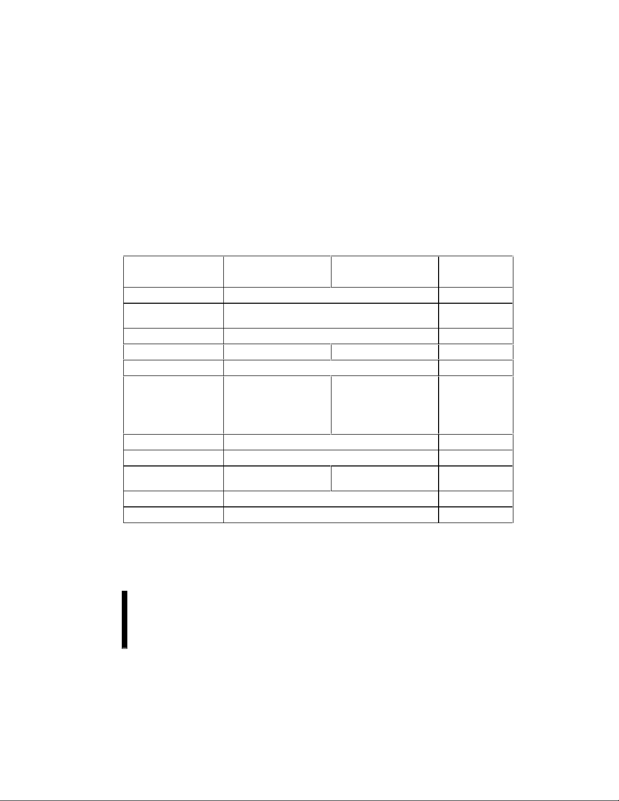
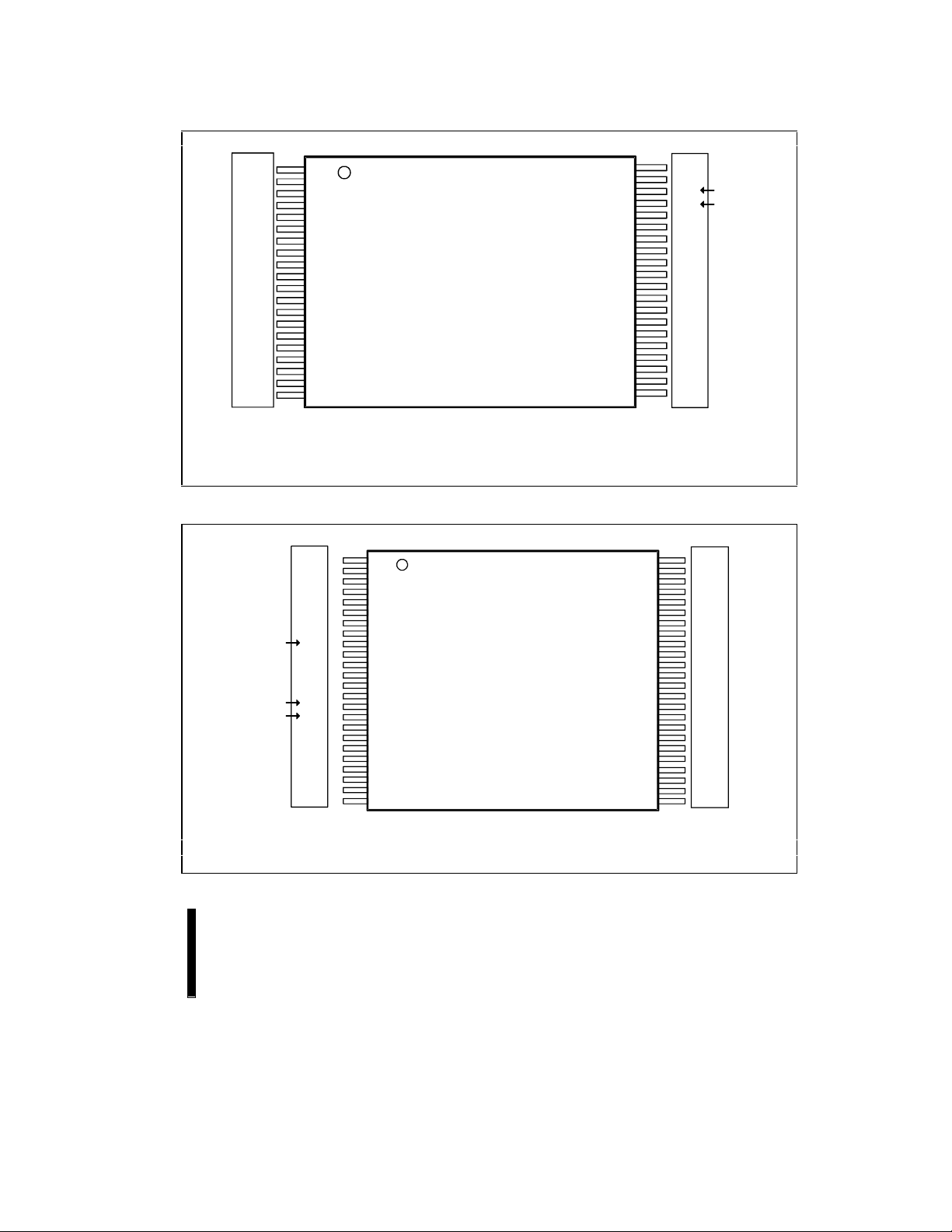
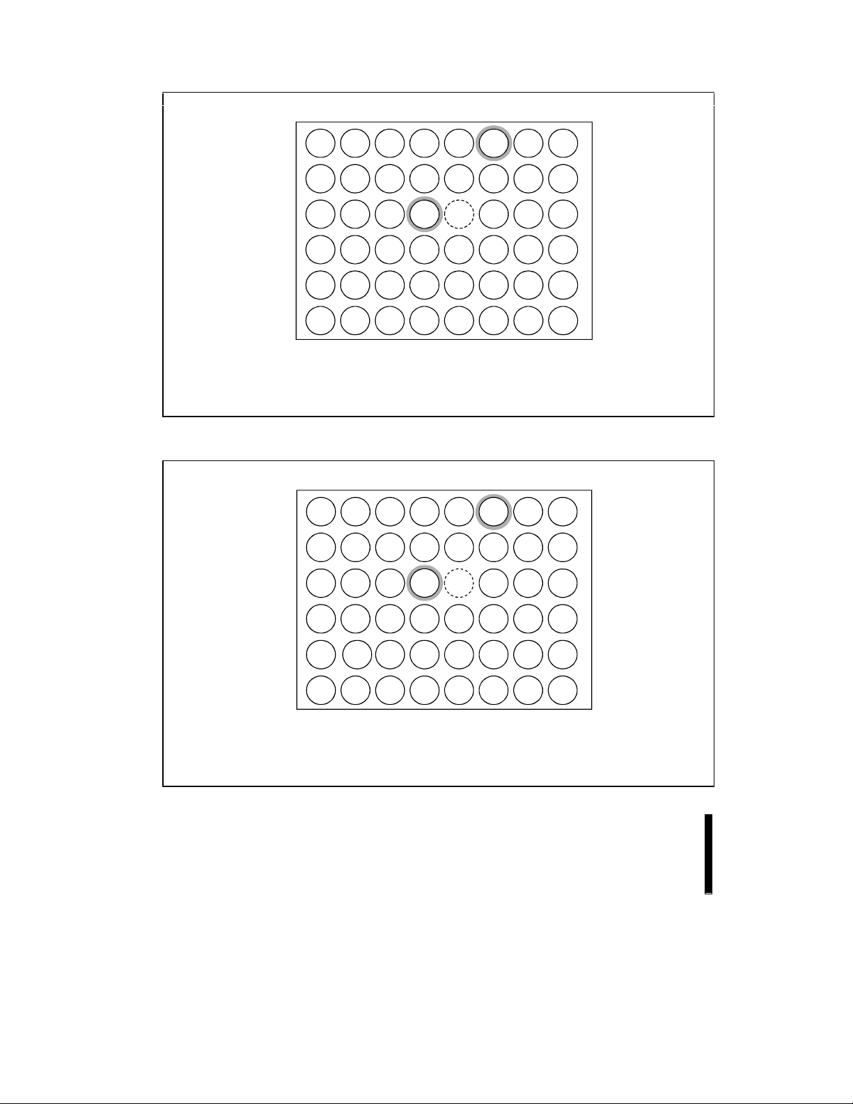
This section provides device pin descriptions and
package pinouts for the 3 Volt Advanced+ Boot
Block flash memory f amily, which is availabl e in 40Lead TSOP (x8, Figure 1), 48-lead TSOP (x16,
Figure 2) and 48-ball µBGA packages (Figures 3
and 4).
2.1 Package Pinouts
In each diagram, upgrade pins from one dens ity to
the next are circled.
PRODUCT PREVIEW
E 3 VOLT ADVANCED+ BOOT BLOCK
A
A
A
A
A
A
A
A
WE#
RP#
V
PP
WP#
A
A
A
A
A
A
A
A
16
15
14
13
12
11
9
8
18
7
6
5
4
3
2
1
1
2
3
4
5
6
7
8
9
10
11
12
13
14
15
16
17
18
19
20
Advanced Boot
40-Lead TSOP
10 mm x 20 mm
TOP VIEW
40
39
38
37
36
35
34
33
32
31
30
29
28
27
26
25
24
23
22
21
A
17
GND
A
20
A
19
A
10
DQ
DQ
DQ
DQ
V
CCQ
V
CC
NC
DQ
DQ
DQ
DQ
OE#
GND
CE#
A
0
16M
8M
7
6
5
4
3
2
1
0
NOTES:
1. 40-Lead TSOP available for 8- and 16-Mbit densities only.
2. Lower densities will have NC on the upper address pins. For example, an 8-Mbit device will have NC on Pin 38.
Figure 1. 40-Lead TSOP Package for x8 Configurations
A
A
15
A
14
A
13
A
12
A
11
A
10
A
9
A
8
A
32M
20
NC
WE#
RP#
V
PP
WP#
A
16M
19
A
8M
18
A
17
A
7
A
6
A
5
A
4
A
3
A
2
A
1
1
2
3
4
5
6
7
8
9
10
11
12
13
14
15
16
17
18
19
20
21
22
23
24
Advanced Boot Block
48-Lead TSOP
12 mm x 20 mm
TOP VIEW
48
47
46
45
44
43
42
41
40
39
38
37
36
35
34
33
32
31
30
29
28
27
26
25
NOTE:
Lower densities will have NC on the upper address pins. For example, an 8-Mbit device will have NC on Pins 9 and 15.
16
V
CCQ
GND
DQ
DQ
DQ
DQ
DQ
DQ
DQ
DQ
V
CC
DQ
DQ
DQ
DQ
DQ
DQ
DQ
DQ
OE#
GND
CE#
A
0
15
7
14
6
13
5
12
4
11
3
10
2
9
1
8
0
Figure 2. 48-Lead TSOP Package for x16 Configurations
PRODUCT PREVIEW
7
3 VOLT ADVANCED+ BOOT BLOCK E
12345678
A
13
A
B
14A10
C
A15A
D
A
16D14D5
E
V
CCQ
F
GND D7D
A
11A8
12A9
D
15D6
VPPWP# A
WE# RP# A
32M
A
20
D
11D2
D
12D3
13D4VCCD10D1
16M
A
19
18A17A5
A
6
D8CE# A
D9D0GND
A
7
4A
A
2
A
A
3
1
0
OE#
NOTES:
1. Shaded connections indicate the upgrade address connections. Lower density devices will not have the upper address
solder balls. Routing is not recommended in this area. A19 is the upgrade address for the 16-Mbit device. A20 is the
upgrade address for the 32-Mbit device.
2. 8-Mbit not available on µBGA* CSP.
Figure 3. x16 48-Ball µBGA* Chip Size Package (Top View, Ball Down)
12345678
A
A14A
12A8
V
PP
WP#
16M
A
A
20
A
7
4
A
B
15A10
A16A
C
D
A
17
E
V
CCQA11D6
F
GND
13A9
NC
D
7
WE#
D
NC
32M
5
RP#
A
21
NC
NC
D4V
A19A
D
2
D
3
CC
18A5
A6A
NC CE#
D
NC
D
NC
A
2
A
3
1
A
0
GND
0
OE#
1
NOTES:
1. Shaded connections indicate the upgrade address connections. Lower density devices will not have the upper address
solder balls. Routing is not recommended in this area. A
upgrade address for the 32-Mbit device.
is the upgrade address for the 16-Mbit device. A
20
21
is the
2. 8-Mbit not available on µBGA* CSP.
Figure 4. x8 48-Ball µBGA* Chip Size Package (Top View, Ball Down)
8
PRODUCT PREVIEW

E 3 VOLT ADVANCED+ BOOT BLOCK
Table 2. 3 Volt Advanced+ Boot Block Pin Descriptions
Symbol Type Name and Function
A0–A
21
DQ0–DQ7INPUT/OUTPUT DATA INPUTS/OUTPUTS: Inputs array data on the second CE# and
DQ8–DQ15INPUT/OUTPUT DATA INPUTS/OUTPUTS: Inputs array data on the second CE# and
CE# INPUT CHIP ENABLE: Activates the internal control logic, input buffers,
OE# INPUT OUTPUT ENABLE: Enables the device’s outputs through the data
WE# INPUT WRITE ENABLE: Controls writes to the Command Register and
RP# INPUT RESET/DEEP POWER-DOWN: Uses two voltage levels (VIL, VIH) to
WP# INPUT WRITE PROTECT: Controls the lock-down function of the flexible
V
CC
INPUT
SUPPLY DEVICE POWER SUPPLY: [2.7 V–3.6 V] Supplies power for device
ADDRESS INPUTS for memory addresses. Addresses are internally
latched during a program or erase cycle.
8-Mbit x 8 A[0-19], 16-Mbit x 8 A[0-20], 32-Mbit x 8 A[0-21]
8-Mbit x 16 A[0-18], 16-Mbit x 16 A[0-19], 32-Mbit x 16 A[0-20]
WE# cycle during a Program command. Inputs commands to the
Command User Interface when CE# and WE# are active. Data is
internally latched. Outputs array, configuration and status register data.
The data pins float to tri-state when the chip is de-selected or the outputs
are disabled.
WE# cycle during a Program command. Data is internally latched.
Outputs array and configuration data. The data pins float to tri-state when
the chip is de-selected. Not included on x8 products.
decoders and sense amplifiers. CE# is active low. CE# high de-selects
the memory device and reduces power consumption to standby levels.
buffers during a read operation. OE# is active low.
memory array. WE# is active low. Addresses and data are latched on
the rising edge of the second WE# pulse.
control reset/deep power-down mode.
When RP# is at logic low, the device is in reset/deep power-down
mode, which drives the outputs to High-Z, resets the Write State
Machine, and minimizes current levels (I
When RP# is at logic high, the device is in standard operation.
When RP# transitions from logic-low to logic-high, the device resets all
blocks to locked and defaults to the read array mode.
Locking feature
When WP# is a logic low, the lock-down mechanism is enabled and
blocks marked lock-down cannot be unlocked through software.
When WP# is logic high, the lock-down mechanism is disabled and
blocks previously locked-down are now locked and can be unlocked and
locked through software. After WP# goes low, any blocks previously
marked lock-down revert to that state.
See Section 3.3 for details on block locking.
operations.
CCD
).
PRODUCT PREVIEW
9

3 VOLT ADVANCED+ BOOT BLOCK E
PP
Table 2. 3 Volt Advanced+ Boot Block Pin Descriptions (Continued)
Symbol Type Name and Function
V
CCQ
V
PP
GND SUPPLY GROUND: For all internal circuitry. All ground inputs must be
NC NO CONNECT: Pin may be driven or left floating.
INPUT I/O POWER SUPPLY: Supplies power for input/output buffers.
[2.7 V–3.6 V] This input should be tied directly to V
CC
.
[1.65 V– 2.5 V] Lower I/O power supply voltage available upon request.
Contact your Intel representative for more information.
INPUT/
SUPPLY
PROGRAM/ERASE POWER SUPPLY: [1.65 V–3.6 V or 11.4 V–12.6 V]
Operates as a input at logic levels to control complete device protection.
Supplies power for accelerated program and erase operations in 12 V ±
5% range. This pin cannot be left floating.
Lower V
PP
≤ V
, to protect all contents against Program and
PPLK
Erase commands.
= VCC for in-system read, program and erase operations. In
Set V
PP
this configuration, V
diode drop from the system supply. Note that if V
signal, V
1.65. That is, V
IH =
can drop as low as 1.65 V to allow for resistor or
is driven by a logic
must remain above 1.65V to perform in-
PP
PP
system flash modifications.
Raise V
environment. Applying 12 V ± 5% to V
to 12 V ± 5% for faster program and erase in a production
PP
can only be done for a
PP
maximum of 1000 cycles on the main blocks and 2500 cycles on the
parameter blocks.
maximum. See Section 3.4 for details on V
VPP may be connected to 12 V for a total of 80 hours
voltage configurations.
PP
connected.
2.2 Block Organization
The 3 Volt Advanced+ Boot Block is an
asymmetrically-blocked architecture that enables
system integration of code and data within a single
flash device. Each block can be erased
independently of the others up to 100,000 times.
For the address locations of each block, see the
memory maps in Appendix E and F.
10
2.2.1 PARAMETER BLOCKS
The 3 Volt Advanced+ Boot Block flash memory
architecture includes parameter blocks to facilitate
storage of frequently updated small parameters
(i.e., data that would normally be stored in an
EEPROM). Each device contains eight parameter
blocks of 8-Kbytes/4-Kwords (8,192 bytes/4,096
words).
2.2.2 MAIN BLOCKS
After the parameter blocks, the remainder of the
array is divided into equal size (64-Kword/32Kword; 65,536 bytes/32,768 words ) main blocks for
data or code storage. Each 8-Mbit, 16-Mbit, or
32-Mbit device contains 15, 31, or 63 main blocks,
respectively.
PRODUCT PREVIEW

E 3 VOLT ADVANCED+ BOOT BLOCK
3.0 PRINCIPLES OF OPERATION
The 3 Volt Advanced+ Boot Block flash memory
family utilizes a CUI and automated algorithms to
simplify program and erase operations. The CUI
allows for 100% CMOS
fixed power supplies during erasure and
programming.
-
level control inputs and
the V
command must be issued t o the CUI to enter the
corresponding mode. Upon initial dev ice power
or after exit from reset, the device automatically
defaults to read array mode.
CE# and OE# must be driven active to obtain dat a
at the outputs. CE# is the device s election control;
voltage. The appropriate read mode
PP
when active it enables the flash memory device.
The internal WSM completely automates program
and erase operations while the CUI si gnals the s tart
of an operation and the status register reports
status. The CUI handles t he WE# interface to the
OE# is the data output control and it drives the
selected memory data ont o the I/ O bus . For all read
modes, WE# and RP# must be at V
illustrates a read cycle.
data and address latches, as well as system status
requests during WSM operation.
3.1 Bus Operation
The 3 Volt Advanced+ Boot Block flash memory
devices read, program and erase in
local CPU or microcontroller. All bus cycles to or
from the flash memory conform to standard
microcontroller bus cycles. Four control pins dictate
the data flow in and out of the flash component:
CE#, OE#, WE# and RP#. These bus operations
are summarized in Table 3.
-
system via the
3.1.2 OUTPUT DISABLE
With OE# at a logic
outputs are disabled. Output pins are placed in a
high
-
impedance state.
3.1.3 STANDBY
Deselecting the device by bri nging CE# to a logic
high level (VIH) places the device in standby mode,
which substantially reduces device power
consumption without any latency for subsequent
read accesses. In standby, outputs are placed in a
3.1.1 READ
The flash memory has four read modes available:
read array, read configuration, read s tatus and read
high-impedance state independent of OE#. If
deselected during program or erase operat ion, the
device continues to c onsume active power unt il the
program or erase operation is complete.
query. These modes are accessi ble independent of
Table 3. Bus Operations
(1)
Mode Note RP# CE# OE# WE# DQ
Read (Array, Status,
Configuration, or Query)
Output Disable 2 V
Standby 2 V
Reset 2,7 V
Write 2,5-7 V
NOTES:
1. 8-bit devices use only DQ[0:7], 16-bit devices use DQ[0:15]
2. X must be V
3. See
4. Manufacturer and device codes may also be accessed in read configuration mode (A
5. Refer to Table 5 for valid D
6. To program or erase the lockable blocks, hold WP# at V
7. RP# must be at GND ± 0.2 V to meet the maximum deep power-down current specified.
, VIH for control pins and addresses.
IL
DC Characteristics
for V
2-4 V
, V
, V
PP1
PP2
, V
PPLK
during a write operation.
IN
IH
IH
IH
IL
IH
, voltages.
PP3
V
IL
V
IL
V
IH
V
IL
V
IH
X X High Z High Z
X X X High Z High Z
V
IL
.
IH
V
IH
1–A20
. Figure 9
IH
-
high level (VIH), the device
DQ
8-15
D
OUT
D
IN
V
IH
V
IH
V
IL
D
High Z High Z
D
= 0). See Table 4.
0–7
OUT
IN
-
up
-
PRODUCT PREVIEW
11

3 VOLT ADVANCED+ BOOT BLOCK E
3.1.4 RESET
From read mode, RP# at V
for time t
IL
PLPH
deselects the memory, places output drivers in a
high
-
impedance state, and turns off all internal
circuits. After return from reset, a time t
PHQV
is
required until the initial read access outputs are
valid. A delay (t
PHWL
or t
) is required after
PHEL
return from reset before a write can be initiated.
After this wake
-
up interval, normal operation is
restored. The CUI resets t o read array mode, and
the status register i s s et t o 80H. This cas e is shown
in Figure 11A.
If RP# is taken low for time t
during a program
PLPH
or erase operation, the operation will be aborted
and the memory contents at the aborted location
(for a program) or block (for an erase) are no longer
valid, since the data may be partially erased or
written. The abort process goes through the
following sequence: When RP# goes low, the
device shuts down the operation in progress, a
process which takes time t
this time t
, the part will either reset to read
PLRH
array mode (if RP# has gone high during t
to complete. After
PLRH
PLRH
Figure 11B) or enter reset mode (if RP# is still logic
low after t
, Figure 11C). In both cases, after
PLRH
returning from an aborted operation, the relevant
time t
PHQV
or t
PHWL/tPHEL
must be waited bef ore a
read or write operation is initiat ed, as discussed in
the previous paragraph. However, in this case,
these delays are referenced to the end of t
PLRH
rather than when RP# goes high.
As with any automated device, it is important to
assert RP# during system reset. When the system
comes out of reset, proc essor expec ts to read from
the flash memory. Automated flash memories
provide status information when read during
program or block erase operations. If a CPU reset
occurs with no flash memory reset, proper CPU
initialization may not occur because the flash
memory may be providing status information
instead of array data. Int el’s flash memories allow
proper CPU initialization following a system reset
through the use of the RP# input. In this application,
RP# is controlled by the same RESET# signal that
resets the system CPU.
addressable memory location. The address and
data buses are latched on the rising edge of the
second WE# or CE# pulse, whichever occ urs first.
Figure 10 illustrates a program and erase operation.
The available commands are shown in Tabl e 6, and
Appendix A provides detailed information on
moving between the different modes of operation
using CUI commands.
There are two commands that modify array data:
Program (40H) and Erase (20H). Writing either of
these commands to the internal Command User
Interface (CUI) initiates a sequence of internally
timed functions that culminate in the c ompletion of
the requested task (unless that operat ion is aborted
by either RP# being driven to V
for t
IL
appropriate suspend command).
3.2 Modes of Operation
The flash memory has four read modes and two
write modes. The read modes are read array, read
configuration, read status, and read query. The
,
write modes are program and block erase. Three
additional modes (erase suspend to program, eras e
suspend to read and program suspend to read) are
available only during suspended operations. These
modes are reached using the commands
summarized in Tables 5 and 6. A comprehensive
chart showing the state transitions is in Appendix A.
3.2.1 READ ARRAY
When RP# transitions from V
device defaults to read array mode and will res pond
to the read control inputs (CE #, address i nputs , and
OE#) without any additional CUI commands.
When the device is in read array mode, four control
signals control data output:
• WE# must be logic high (V
• CE# must be logic low (V
• OE# must be logic low (V
• RP# must be logic high (V
(reset) to VIH, the
IL
)
IH
)
IL
)
IL
)
IH
PLRH
or an
-
3.1.5 WRITE
A write takes place when bot h CE# and WE# are
low and OE# is high. Commands are written to the
Command User Interface (CUI) using standard
microprocessor write timings to control flash
operations. The CUI does not occupy an
12
In addition, the address of the desired l ocat ion mus t
be applied to the address pins. If the dev ice is not
in read array mode, as would be t he case after a
program or erase operation, the Read Array
command (FFH) must be written to the CUI before
array reads can take place.
PRODUCT PREVIEW

E 3 VOLT ADVANCED+ BOOT BLOCK
3.2.2 READ CONFIGURATION
The Read Configuration mode outputs the
manufacturer/device identifier. The device is
switched to this mode by writing the Read
Configuration command (90H). Once i n this mode,
read cycles from addresses shown in Table 4
retrieve the specified i nformation. To return to read
array mode, write the Read Array command (FFH).
The Read Configuration mode outputs three types
of information: the manufacturer/device identifier,
the block locking status , and the protec tion regis ter.
The device is switched to this mode by writ ing the
Read Configuration command (90H). Once in this
mode, read cycles from addresses shown in Table
4 retrieve the specified information. To return to
read array mode, write the Read Array command
(FFH).
Table 4. Read Configuration Table
Item Address Data
Manufacturer Code (x16) 00000 0089
Manufacturer Code (x8) 00000 89
Device ID (See Appendix G) 00001 ID
Block Lock Configuration
• Block Is Unlocked DQ0 = 0
• Block Is Locked DQ0 = 1
• Block Is Locked-Down DQ1 = 1
Protection Register Lock
Protection Register (x16) 81-88 PR
Protection Register (x8) (App. H) PR
NOTES:
1. “XX” specifies the block address of lock configuration
being read.
2. See Section 3.3.4 for valid lock status outputs.
3. See Section 3.4 for protection register information.
4. Other locations within the configuration address space
are reserved by Intel for future use.
3.2.3 READ STATUS REGISTER
The status register indicates the status of device
operations, and the success/failure of that
operation. The Read Status Register (70H)
2
3
(1)
XX002
80 PR-LK
LOCK
command causes subsequent reads to output data
from the status register until another command is
issued. To return to reading from t he array, issue a
Read Array (FFH) command.
The status register bits are output on DQ
The upper byte, DQ
Read Status Register command.
The contents of the st atus register are latched on
the falling edge of OE# or CE#, whichever oc curs
last. This prevents possible bus errors which might
occur if status regi ster content s change while being
read. CE# or OE# must be toggled with each
subsequent status read, or the status register will
not indicate completion of a program or erase
operation.
When the WSM is active, SR.7 will indicate the
status of the WSM; t he remaining bits in the st atus
register indicate whether the WSM was successful
in performing the desired operation (see Table 7).
3.2.3.1 Clearing the Status Register
The WSM sets status bits 1 through 7 to “1,” and
clears bits 2, 6 and 7 to “0, ” but cannot clear status
bits 1 or 3 through 5 to “0.” Becaus e bits 1, 3, 4 and
5 indicate various error conditions, these bits can
only be cleared through the use of the Clear Status
Register (50H) command. By allowing the system
software to control the resetting of these bits,
several operations may be performed (such as
cumulatively programming several addresses or
erasing multiple blocks in sequence) before reading
the status register t o determine if an error occurred
during that series. Clear the St atus Register before
beginning another command or sequence. Note
that the Read Array command must be issued
before data can be read from the memory array.
Resetting the device also clears the status register.
3.2.4 READ QUERY
The Read Query mode outputs Common Flash
Interface (CFI) data when the devi ce is read. This
can be accessed by writing the Read Query
Command (98H). The CFI data structure contains
information such as bloc k size, density, c ommand
set and electrical specificat ions. Once i n this mode,
read cycles from addresses shown in Appendi x C
retrieve the specified i nformation. To return to read
array mode, write the Read Array command (FFH).
–DQ15, outputs 00H during a
8
–DQ7.
0
PRODUCT PREVIEW
13

3 VOLT ADVANCED+ BOOT BLOCK E
3.2.5 PROGRAM MODE
-
Programming is executed using a two
write
sequence. The Program Setup command (40H) is
written to the CUI foll owed by a sec ond write which
specifies the address and data to be programmed.
The WSM will execute a sequence of internally
timed events to program desired bits of the
addressed location, then verify the bits are
sufficiently programmed. Programming the memory
results in specific bits within an address location
being changed to a “0.” If the user attempts to
program “1”s, the memory cell contents do not
change and no error occurs.
The status register indicates programming status:
while the program sequence execut es, status bit 7
is “0.” The status regis ter can be poll ed by toggling
either CE# or OE#. While programming, the only
valid commands are Read Status Register,
Program Suspend, and Program Resume.
When programming is complete, the Program
Status bits shoul d be checked. If the programming
operation was unsuccessf ul, bit SR.4 of the status
register is set to indi cate a program f ailure. If S R.3
is set then V
was not within acceptable l i m i ts, and
PP
the WSM did not execute t he program command. If
SR.1 is set, a program operation was att empted on
a locked block and the operation was aborted.
The status register should be cleared before
attempting the next operat ion. Any CUI instruction
can follow after programming is completed;
however, to prevent inadvertent status register
reads, be sure to reset the CUI to read array mode.
3.2.5.1 Suspending and Resuming
Program
The Program Suspend command halts an in
progress program operation so that data can be
read from other locations of memory. Once the
programming process starts, writing the Program
Suspend command to the CUI requests that the
WSM suspend the program sequence (at
predetermined points in the program algorithm).
The device continues to output status register data
after the Program Suspend command is written.
Polling status register bits SR.7 and SR.2 will
determine when the program operation has been
suspended (both will be set to “1”). t
WHRH1/tEHRH1
specify the program suspend latency.
A Read Array command can now be writt en to the
CUI to read data from blocks other than that which
is suspended. The only other valid commands,
while program is suspended, are Read Status
Register, Read Configuration, Read Query, and
Program Resume. After the Program Resume
command is written to t he flash memory, the WSM
will continue with the programming process and
status register bits SR.2 and S R.7 will aut omatic ally
be cleared. The device automatically outputs s tatus
register data when read (see Figure 13 in Appendix
B,
Program Suspend/Resume Flowchart
Program Resume command is written. V
remain at the same V
level used for program
PP
while in program suspend mode. RP# must also
remain at V
.
IH
3.2.6 ERASE MODE
To erase a block, write the Erase Set
Confirm commands to the CUI, along with an
address identifying the block to be erased. This
address is latched internally when the Erase
Confirm command is iss ued. Block erasure results
in all bits within the block being s et to “1.” Only one
block can be erased at a time. The WSM will
execute a sequence of internally timed events to
program all bits within the block to “0, ” erase all bit s
within the block to “1,” t hen verify t hat all bits within
the block are sufficiently erased. While the erase
executes, status bit 7 is a “0.”
When the status register indicates that erasure is
complete, check the erase status bit to verify that
the erase operation was successful. If the Erase
operation was unsuccessful, SR.5 of the status
register will be set to a “1,” indicating an erase
failure. If V
the Erase Confirm command was issued, t he WSM
will not execute the erase sequence; instead, SR.5
-
of the status register is set to indicate an erase
was not within acceptable l imits after
PP
error, and SR.3 is set to a “1” t o identify that V
supply voltage was not within acceptable limits.
After an erase operation, clear the status register
(50H) before attempting the next operation. Any
CUI instruction can follow after erasure is
completed; however, to prevent inadvertent status
register reads, it is adv isable to place the flash in
read array mode after the erase is complete.
) after the
must
PP
-
up and Erase
PP
14
PRODUCT PREVIEW

E 3 VOLT ADVANCED+ BOOT BLOCK
3.2.6.1 Suspending and Resuming Erase
Since an erase operation requires on the order of
seconds to complete, an Erase Suspend c ommand
is provided to allow erase
order to read data from or program data to another
block in memory. Once the erase sequence is
started, writing the Erase Suspend com mand to the
CUI suspends the erase sequence at a
predetermined point in the erase algorithm. The
status register will indicate if/when the erase
operation has been suspended. Erase suspend
latency is specified by t
Command Notes Oper Addr Data Oper Addr Data
Read Array 4 Write X FFH
Read Configuration 2, 4 Write X 90H Read IA ID
Read Query 2, 4 Write X 98H Read QA QD
Read Status Register 4 Write X 70H Read X SRD
Clear Status Register 4 Write X 50H
Program 3,4 Write X 40H/10H Write PA PD
Block Erase/Confirm 4 Write X 20H Write BA D0H
Program/Erase Suspend 4 Write X B0H
Program/Erase Resume 4 Write X D0H
Lock Block 4 Write X 60H Write BA 01H
Unlock Block 4 Write X 60H Write BA D0H
Lock-Down Block 4 Write X 60H Write BA 2FH
Protection Program 4 Write X C0H Write PA PD
X = Don’t Care PA = Prog Addr BA = Block Addr IA = Identifier Addr. QA = Query Addr.
SRD = Status Reg. Data PD = Prog Data ID = Identifier Data QD = Query Data
NOTES:
1. Bus operations are defined in Table 3.
2. Following the Read Configuration or Read Query commands, read operations output device configuration or CFI query
information, respectively. See Section 3.2.2 and 3.2.4.
3. Either 40H or 10H command is valid, but the Intel standard is 40H.
4. When writing commands, the upper data bus [DQ
-
sequence interruption in
WHRH2/tEHRH2
.
Table 5. Command Bus Definitions
–DQ15] should be either VIL or VIH, to minimize current draw.
8
A Read Array/Program command can now be
written to the CUI to read/program data from/to
blocks other than that which is suspended. This
nested Program command can subsequently be
suspended to read yet another location. The only
valid commands while erase is suspended are
Read Status Register, Read Configuration, Read
Query, Program Setup, Program Resume, Erase
Resume, Lock Bloc k, Unlock Block and Lock -Down
Block. During erase suspend mode, the c hip c an be
placed in a pseudo
V
. This reduces active current consumption.
IH
Erase Resume continues t he eras e s equenc e when
CE# = V
operation, the status register must be read and
cleared before the next instruction is issued.
First Bus Cycle Second Bus Cycle
. As with the end of a standard erase
IL
-
standby mode by taking CE# to
PRODUCT PREVIEW
15

3 VOLT ADVANCED+ BOOT BLOCK E
Table 6. Command Codes and Descriptions
Code Device Mode Description
FF Read Array Places device in read array mode, such that array data will be output on the
40 Program
Set-Up
20 Erase
Set-Up
D0 Erase Confirm
Program/Erase
Resume
Unlock Block
B0 Program
Suspend
Erase
Suspend
70 Read Status
Register
50 Clear Status
Register
90 Read
Configuration
60 Configuration
Set-Up
01 Lock-Block If the previous command was Configuration Set-Up, the CUI will latch the
data pins.
This is a two-cycle command. The first cycle prepares the CUI for a program
operation. The second cycle latches addresses and data information and
initiates the WSM to execute the Program algorithm. The flash outputs status
register data when CE# or OE# is toggled. A Read Array command is required
after programming to read array data. See Section 3.2.5.
Prepares the CUI for the Erase Confirm command. If the next command is not
an Erase Confirm command, then the CUI will (a) set both SR.4 and SR.5 of the
status register to a “1,” (b) place the device into the read status register mode,
and (c) wait for another command. See Section 3.2.6.
If the previous command was an Erase Set-Up command, then the CUI will
close the address and data latches, and begin erasing the block indicated on the
address pins. During program/erase, the device will respond only to the Read
Status Register, Program Suspend and Erase Suspend commands and will
output status register data when CE# or OE# is toggled.
If a program or erase operation was previously suspended, this command will
resume that operation.
If the previous command was Configuration Set-Up, the CUI will latch the
address and unlock the block indicated on the address pins. If the block had
been previously set to Lock-Down, this operation will have no effect. (Sect. 3.3)
Issuing this command will begin to suspend the currently executing
program/erase operation. The status register will indicate when the operation
has been successfully suspended by setting either the program suspend (SR.2)
or erase suspend (SR.6) and the WSM Status bit (SR.7) to a “1” (ready). The
WSM will continue to idle in the SUSPEND state, regardless of the state of all
input control pins except RP#, which will immediately shut down the WSM and
the remainder of the chip if RP# is driven to V
3.2.6.1.
This command places the device into read status register mode. Reading the
device will output the contents of the status register, regardless of the address
presented to the device. The device automatically enters this mode after a
program or erase operation has been initiated. See Section 3.2.3.
The WSM can set the Block Lock Status (SR.1) , VPP Status (SR.3), Program
Status (SR.4), and Erase Status (SR.5) bits in the status register to “1,” but it
cannot clear them to “0.” Issuing this command clears those bits to “0.”
Puts the device into the Read Configuration mode, so that reading the device
will output the manufacturer/device codes or block lock status. Section 3.2.2.
Prepares the CUI for changes to the device configuration, such as block locking
changes. If the next command is not Block Unlock, Block Lock, or Block LockDown, then the CUI will set both the Program and Erase Status register bits to
indicate a command sequence error. See Section 3.3.
address and lock the block indicated on the address pins. (Section 3.3)
. See Sections 3.2.5.1 and
IL
16
PRODUCT PREVIEW

E 3 VOLT ADVANCED+ BOOT BLOCK
Table 6. Command Codes and Descriptions (Continued)
Code Device Mode Description
2F Lock-Down If the previous command was a Configuration Set-Up command, the CUI will
98 Read
Query
C0 Protection
Program
Setup
10 Alt. Prog Set-Up Operates the same as Program Set-up command. (See 40H/Program Set-Up)
00 Invalid/
Reserved
NOTE:
See Appendix A for mode transition information.
latch the address and lock-down the block indicated on the address pins.
(Section 3.3)
Puts the device into the Read Query mode, so that reading the device will
output Common Flash Interface information. See Section 3.2.4 and Appendix C.
This is a two-cycle command. The first cycle prepares the CUI for an program
operation to the Protection Register. The second cycle latches addresses and
data information and initiates the WSM to execute the Protection Program
algorithm to the Protection Register. The flash outputs status register data when
CE# or OE# is toggled. A Read Array command is required after programming
to read array data. See Section 3.4.
Unassigned commands that should not be used. Intel reserves the right to
redefine these codes for future functions.
PRODUCT PREVIEW
17

3 VOLT ADVANCED+ BOOT BLOCK E
PP
level. The WSM interrogates V
is also checked before the
and V
Table 7. Status Register Bit Definition
WSMS ESS ES PS VPPS PSS BLS R
76543210
NOTES:
SR.7 WRITE STATE MACHINE STATUS
1 = Ready (WSMS)
0 = Busy
SR.6 = ERASE-SUSPEND STATUS (ESS)
1 = Erase Suspended
0 = Erase In Progress/Completed
SR.5 = ERASE STATUS (ES)
1 = Error In Block Erase
0 = Successful Block Erase
SR.4 = PROGRAM STATUS (PS)
1 = Error in Programming
0 = Successful Programming
SR.3 = VPP STATUS (VPPS)
1 = V
0 = V
Low Detect, Operation Abort
PP
OK
PP
SR.2 = PROGRAM SUSPEND STATUS
(PSS)
1 = Program Suspended
0 = Program in Progress/Completed
SR.1 = BLOCK LOCK STATUS
1 = Prog/Erase attempted on a locked
block; Operation aborted.
0 = No operation to locked blocks
SR.0 = RESERVED FOR FUTURE
ENHANCEMENTS (R)
Check Write State Machine bit first to determine Word
Program or Block Erase completion, before checking
Program or Erase Status bits.
When Erase Suspend is issued, WSM halts execution
and sets both WSMS and ESS bits to “1.” ESS bit
remains set to “1” until an Erase Resume command is
issued.
When this bit is set to “1,” WSM has applied the max.
number of erase pulses to the block and is still unable to
verify successful block erasure.
When this bit is set to “1,” WSM has attempted but failed
to program a word/byte.
The V
of V
status bit does not provide continuous indication
PP
level only after
PP
the Program or Erase command sequences have been
entered, and informs the system if V
switched on. The V
PP
has not been
PP
operation is verified by the WSM. The VPPstatus bit is
not guaranteed to report accurate feedback between
V
PPLK
PP1
Min.
When Program Suspend is issued, WSM halts execution
and sets both WSMS and PSS bits to “1.” PSS bit
remains set to “1” until a Program Resume command is
issued.
If a program or erase operation is attempted to one of the
locked blocks, this bit is set by the WSM. The operation
specified is aborted and the device is returned to read
status mode.
This bit is reserved for future use and should be masked
out when polling the status register.
18
PRODUCT PREVIEW

E 3 VOLT ADVANCED+ BOOT BLOCK
3.3 Flexible Block Locking
The Intel® 3 Volt Advanced+ Boot Block products
offer an instant, individual block locking scheme
that allows any block t o be locked or unlocked with
no latency, enabling instant code and data
protection.
This locking scheme offers t wo levels of protec tion.
The first level allows software-only control of bloc k
locking (useful for data blocks that change
frequently), while the second level requires
hardware interaction before locki ng can be changed
(useful for code blocks that change infrequently).
The following sections will discuss the operat ion of
the locking system. The term “state [XYZ]” will be
used to specify locking states; e.g., “state [001],”
where X = value of WP#, Y = bit DQ
Lock status regist er, and Z = bit DQ
Lock status register. Table 9 defines all of these
possible locking states.
3.3.1 LOCKING OPERATION
The following concisely summarizes the locking
functionality.
• All blocks power-up locked, then can be
unlocked or locked with the Unlock and Lock
commands.
• The Lock-Down command locks a block and
prevents it from being unlocked when WP# = 0.
When WP# = 1, Lock-Down is overridden
and commands can unlock/lock lockeddown blocks.
When WP# returns to 0, locked-down
blocks return to Lock-Down.
Lock-Down is cleared only when t he device
is reset or powered-down.
The locking status of each block can s et t o Loc ked,
Unlocked, and Lock-Down, each of which will be
described in the following sections. A
comprehensive state table f or the locking functions
is shown in Table 9, and a flowchart for locking
operations is shown in Figure 16.
of the Block
1
of the Block
0
3.3.2 LOCKED STATE
The default status of all blocks upon power-up or
reset is locked (states [001] or [101]). Locked
blocks are fully protected from alteration. Any
program or erase operations attempted on a l ocked
block will return an error on bit SR.1 of the status
register. The status of a locked block can be
changed to Unlocked or Lock-Down using the
appropriate software commands. An Unlocked
block can be locked by wri ting the Lock command
sequence, 60H followed by 01H.
3.3.3 UNLOCKED STATE
Unlocked blocks (states [000], [100], [110]) can be
programmed or erased. All unlocked blocks return
to the Locked state when the device is reset or
powered down. The status of an unlocked block can
be changed to Locked or Locked-Down using the
appropriate software commands. A Locked block
can be unlocked by writing the Unlock command
sequence, 60H followed by D0H.
3.3.4 LOCK-DOWN STATE
Blocks that are Locked-Down (state [011]) are
protected from program and erase operations (just
like Locked blocks), but their protection status
cannot be changed using software commands
alone. A Locked or Unlocked bloc k can be Lock eddown by writing the Lock-Down command
sequence, 60H followed by 2FH. Locked-Down
blocks revert to the Locked state when the device is
reset or powered down.
The Lock-Down function is dependent on the WP#
input pin. When WP# = 0, blocks in Lock-Down
[011] are protected from program, erase, and loc k
status changes. When WP# = 1, the Lock-Down
function is disabled ([ 111]) and locked-down blocks
can be individually unlock ed by soft ware command
to the [110] state, where they can be erased and
programmed. These blocks can then be relocked
[111] and unlocked [110] as desired while WP#
remains high. When WP# goes low, blocks that
were previously locked-down return to the
Lock-Down state [011] regardless of any changes
made while WP# was high. Device reset or powerdown resets all blocks, including those in LockDown, to Locked state.
PRODUCT PREVIEW
19

3 VOLT ADVANCED+ BOOT BLOCK E
3.3.5 READING A BLOCK’S LOCK STATUS
The lock status of ev ery block can be read in the
Configuration Read mode of the device. To enter
this mode, write 90H to the device. Subsequent
reads at Block Address + 00002 will out put the lock
status of that block . The lock status is represented
by the lowest two output pins , DQ
and DQ1. DQ
0
indicates the Block Lock/Unlock status and is set by
the Lock command and cleared by the Unlock
command. It is also automat ical ly set when entering
Lock-Down. DQ
indicates Lock-Down status and i s
1
set by the Lock-Down command. It cannot be
cleared by software, only by devic e reset or powerdown.
Table 8. Block Lock Status
Item Address Data
Block Lock Configuration XX002 LOCK
• Block Is Unlocked DQ0 = 0
• Block Is Locked DQ0 = 1
• Block Is Locked-Down DQ1 = 1
3.3.6 LOCKING OPERATIONS DURING
ERASE SUSPEND
Changes to block lock status can be performed
during an erase suspend by using the standard
locking command sequences to unlock, lock, or
lock-down a block. This i s useful in the c ase when
another block needs to be updated while an erase
operation is in progress.
the lock status will be changed. After completing
any desired lock, read, or program operations,
resume the erase operation with the Eras e Resume
command (D0H).
If a block is locked or locked-down during a
suspended erase of the same block, the locking
status bits will be changed immediat ely, but when
0
the erase is resumed, the erase operation will
complete.
Locking operations cannot be performed during a
program suspend. Refer to Appendix A for detailed
information on which commands are valid during
erase suspend.
3.3.7 STATUS REGISTER ERROR CHECKING
Using nested locking or program command
sequences during erase suspend can introduce
ambiguity into status register results.
Since locking changes are perf ormed using a two
cycle command sequence, e.g., 60H followed by
01H to lock a block, following the Configuration
Setup command (60H) with an invalid comm and will
produce a lock command error (SR. 4 and SR.5 wi ll
be set to 1) in the status register. If a lock
command error occurs during an erase suspend,
SR.4 and SR.5 will be set to 1, and will remain at 1
after the erase is resumed. When erase is
complete, any possible error during the erase
cannot be detected via the s tatus register becaus e
of the previous locking command error.
To change block locking during an erase operation,
first write the erase s uspend command (B0H), then
check the status register until it indicates that the
erase operation has been suspended. Next write
the desired lock command sequence t o a block and
20
A similar situation happens if an error occ urs during
a program operation error nested within an erase
suspend.
PRODUCT PREVIEW

E 3 VOLT ADVANCED+ BOOT BLOCK
Table 9. Block Locking State Transitions
Current State Erase/Prog Lock Command Input Result [Next State]
WP# DQ1DQ
000 “Unlocked” Yes Goes To [001] No Change Goes To [011]
0 0 1 “Locked” (Default) No No Change Goes To [000] Goes To [011]
0 1 1 “Locked-Down” No No Change No Change No Change
1 0 0 “Unlocked” Yes Goes To [101] No Change Goes To [111]
1 0 1 “Locked” No No Change Goes To [100] Goes To [111]
1 1 0 Lock-Down Disabled Yes Goes To [111] No Change Goes To [111]
1 1 1 Lock-Down Disabled No No Change Goes To [110] No Change
NOTES:
1. In this table, the notation [XYZ] denotes the locking state of a block, where X = WP#, Y = DQ
locking state of a block is defined by the state of WP# and the two bits of the block lock status (DQ
a block is locked (1) or unlocked (0). DQ
2. At power-up or device reset, all blocks default to Locked state [001] (if WP# = 0). Holding WP# = 0 is the recommended
default.
3. The “Erase/Program Allowed?” column shows whether erase and program operations are enabled (Yes) or disabled (No)
in that block’s current locking state.
4. The “Lock Command Input Result [Next State]” column shows the result of writing the three locking commands (Lock,
Unlock, Lock-Down) in the current locking state. For example, “Goes To [001]” would mean that writing the command to a
block in the current locking state would change it to [001].
0
Name Allowed? Lock Unlock Lock-Down
, and Z = DQ0. The current
1
, DQ1). DQ0 indicates if
indicates if a block has been locked-down (1) or not (0).
1
0
3.4 128-Bit Protection Register
The Advanced+ Boot Block arc hitecture includes a
128-bit protection register than can be used to
increase the security of a system design. For
example, the number contained in the protection
register can be used to “mate” the f lash component
with other system com ponents such as the CPU or
ASIC, preventing device substitution. Additional
application information can be found in Intel
application note
Advanced+ Boot Block Flash Memory Architecture
The 128-bits of the protection register are divided
into two 64-bit segments. One of the segments is
programmed at the Intel fact ory wit h a unique 64-bit
number, which is unchangeable. The other segment
is left blank for customer designs to program as
desired. Once the customer segment is
programmed, it can be locked to prevent
reprogramming.
AP-657 Designing with the
PRODUCT PREVIEW
3.4.1 READING THE PROTECTION
The protection register is read in the conf iguration
read mode. The device is switc hed to this mode by
writing the Read Configuration command (90H).
Once in this mode, read cycles from addresses
shown in Appendix H retrieve the specified
information. To return to read array mode, write t he
Read Array command (FFH).
.
3.4.2 PROGRAMMING THE PROTECTION
The protection register bits are programmed us ing
the two-cycle Protection Program command. The
64-bit number is programmed 16 bits at a time for
word-wide parts and eight bits at a time for bytewide parts. First write t he Prot ect ion Program Set up
command, C0H. The next write to the device will
latch in address and data and program the specified
location. The allowable addresses are shown in
Appendix H. See Figure 17 for the
Register Programming Flowchart
REGISTER
REGISTER
.
Protection
21

3 VOLT ADVANCED+ BOOT BLOCK E
Any attempt to address Protection Program
commands outside the defined protection register
address space will result in a Stat us Register error
(Program Error bit SR.4 will be set to 1). Attempting
to program or to a previously locked protection
register segment will result in a status register error
(program error bit SR.4 and lock error bit SR.1 will
be set to 1).
3.4.3 LOCKING THE PROTECTION
REGISTER
The user-programmable segment of the protection
register is lockable by programming Bit 1 of the
PR-LOCK location to 0. Bit 0 of this location is
programmed to 0 at the Intel factory to prot ect the
unique device number. This bit is set using the
Protection Program comm and to program “FFFD” to
the PR-LOCK location. Af ter these bits have been
programmed, no further changes can be made to
the values stored in the protection register.
Protection Program comm ands to a locked section
will result in a status register error (Program Error
bit SR.4 and Lock Error bit SR.1 will be set to 1).
Protection register lockout state is not reversible.
88H
4 Words
User Programmed
85H
84H
4 Words
Factory Programmed
81H
1 Word Lock
80H
0645_05
Figure 5. Protection Register Memory Map
3.5 VPP Program and Erase
Voltages
Intel’s 3 Volt Advanced+ Boot Block products
provide in-system writes plus a V
production programming and complete write
protection.
pin for 12 V
PP
3.5.1 EASY-12 V OPERATION FOR FAST
MANUFACTURING PROGRAMMING
Intel’s 3 Volt Advanced+ Boot Block products
provide in-system programming and erase in the
2.7 V–3.6 V range. For fast production
programming, 3 Volt Advanced+ Boot Block
includes a low-cost, backward-compatible 12 V
programming feature.
When V
and erase current is drawn through the V
Note that if V
V
IH =
is between 1.65 V and 3.6 V, all program
PP
is driven by a logic signal,
1.65 V. That is, V
PP
must remain above 1.65 V
PP
CC
pin.
to perform in-system flash modifications. When V
is connected to a 12 V power supply, the device
draws program and erase current directl y from the
V
pin. This eliminates the need for an external
PP
switching transistor to control the voltage V
PP
Figure 6 shows examples of how the flash power
supplies can be configured for various usage
models.
The 12 V V
mode enhances programming
PP
performance during the short period of time typically
found in manufacturing processes; however, it is
not intended for extended use. 12 V may be applied
to V
during program and erase operations for a
PP
maximum of 1000 cycles on the main blocks and
2500 cycles on the parameter blocks. V
may be
PP
connected to 12 V for a total of 80 hours max imum.
Stressing the devic e beyond these limits may cause
permanent damage.
3.5.2 V
≤ V
PP
PROTECTION
FOR COMPLETE
PPLK
In addition to the flexible block locking, the V
programming voltage can be held low for absolut e
hardware write protection of all blocks in the flash
device. When V
is below V
PP
, any program or
PPLK
erase operation will result in a error, prompt ing the
corresponding status register bit (SR.3) to be set.
3.5.3 V
The V
PP
USAGE
PP
pin is used for two funct i ons : Absolute data
protection and fast production programming.
When V
PP
≤ V
, then all program or erase
PPLK
operations to the device are inhibited, providing
absolute data protection.
PP
.
PP
22
PRODUCT PREVIEW

E 3 VOLT ADVANCED+ BOOT BLOCK
System Supply
12 V Supply
10 K
Ω
12 V Fast Programming
Complete Write Protection When V
System Supply
(Note 1)
12 V Supply
12 V Fast Programming
Full Array Protection Unavailable
NOTE:
1. A resistor can be used if the VCC supply can sink adequate current based on resistor value. See AP-657
the Advanced+ Boot Block Flash Memory Architecture
Figure 6. Example Power Supply Configurations
When V
manufacturing situations , the devi ce direct ly appli es
the high voltage to achieve faster program and
erase.
Designing for in-system writes to the flash memory
requires special consideration of power supply
traces by the printed circuit board designer.
Adequate power supply traces, and decoupling
capacitors placed adjacent to the component, will
decrease spikes and overshoots.
is raised to 12 V, such as in a
PP
V
CC
V
PP
≠ 12 V
PP
V
CC
V
PP
System Supply
Prot#
(Logic Signal)
Low-Voltage Programming Only
Logic Control of Complete Device Protection
System Supply
Low-Voltage Programming Only
Full Array Protection Unavailable
for details.
3.6.1 ACTIVE POWER (Program/Erase/Read)
With CE# at a logic
high level, the device is in the ac ti ve m ode. Refer t o
the DC Characteristic tables for I
Active power is the largest contributor to overall
system power consumption. Minimizing the active
current could have a profound effect on system
power consumption, especi ally for battery
devices.
V
CC
V
PP
V
CC
V
PP
-
low level and RP# at a logic
CC
0645_06
Designing with
current values.
-
operated
-
3.6 Power Consumption
Intel’s flash devices have a tiered approach to
power savings that can significantly reduce ov erall
system power consumption. The Automatic Power
Savings (APS) feature reduces power consumption
when the device is selec ted but idle. If the CE# is
deasserted, the flash enters its standby mode,
where current consumption is even lower. The
combination of these features can minimize
memory power consumption, and therefore, overall
system power consumption.
PRODUCT PREVIEW
3.6.2 AUTOMATIC POWER SAVINGS (APS)
-
Automatic Power Savings provides low
operation during read mode. After data is read from
the memory array and the address lines are
quiescent, APS circuitry places the device in a
mode where typical current is comparable to I
The flash stays in t his st atic s tate wi th outputs val id
until a new location is read.
3.6.3 STANDBY POWER
-
With CE# at a logic
read mode, the flash memory i s in standby mode,
which disables much of the device’s circuitry and
high level (VIH) and device in
power
CCS
23
.

3 VOLT ADVANCED+ BOOT BLOCK E
substantially reduces power consumption. Outputs
are placed in a high
-
impedance state independent
of the status of the OE# signal. I f CE# t ransiti ons to
a logic
-
high level during erase or program
operations, the device will continue to perform the
operation and consume corresponding act iv e power
until the operation is completed.
System engineers should anal yz e the breakdown of
standby time versus active time and quantify the
respective power consumption in each mode for
their specific application. This will provide a more
accurate measure of applic ation
-
specific power and
energy requirements.
3.6.4 DEEP POWER-DOWN MODE
The deep power-down mode is activated when
RP#
(GND ± 0.2 V). During read modes, RP#
= VIL
going low de-selects the memory and places the
outputs in a high impedance s tate. Recovery from
deep power-down requires a minimum time of t
for read operations and t
PHWL/tPHEL
PHQV
for write
operations.
During program or erase modes, RP# transi tioning
low will abort the in-progress operation. The
memory contents of the addres s being program med
or the block being erased are no longer vali d as the
data integrity has been comprom ised by the abort.
During deep power-down, all internal circuits are
switched to a low power savings mode (RP#
transitioning to V
or turning off power to the devic e
IL
clears the status register).
proper CPU/flash initialization following system
reset.
System designers must guard against spurious
writes when V
voltages are above V
CC
LKO
. Since
both WE# and CE# must be low for a command
write, driving either signal to V
will inhibit writ es to
IH
the device. The CUI architecture prov ides additi onal
protection since alterat ion of memory contents c an
only occur after successful completion of the twostep command sequences. The device is also
disabled until RP# is brought to V
, regardless of
IH
the state of its c ontrol inputs. By holding the devic e
in reset (RP# connected to system PowerGood)
during power-up/down, invalid bus conditi ons during
power-up can be masked, providing yet another
level of memory protection.
3.7.2 V
, VPP AND RP# TRANSITIONS
CC
The CUI latches commands as issued by system
software and is not altered by V
or CE#
PP
transitions or WSM actions. Its default state upon
power-up, after exit from reset mode or after V
transitions above V
(Lockout voltage), is read
LKO
CC
array mode.
After any program or block erase operation is
complete (even after V
V
), the CUI must be reset t o read array mode
PPLK
transitions down to
PP
via the Read Array command if access to the fl ash
memory array is desired.
3.8 Power Supply Decoupling
3.7 Power-Up/Down Operation
The device is protected against accidental block
erasure or programming during power transitions.
Power supply sequencing is not required, since the
device is indifferent as to which power supply , V
or VCC, powers-up first.
3.7.1 RP# CONNECTED TO SYSTEM RESET
The use of RP# during system reset is important
with automated program/erase devices since the
system expects to read from the flash memory
when it comes out of res et. If a CPU reset occ urs
without a flash memory reset, proper CPU
initialization will not occur because the flash
memory may be providing status information
instead of array data. Int el recommends c onnecting
RP# to the system CPU RESET# signal to allow
24
PP
Flash memory’s power switching characteristics
require careful device decoupling. System
designers should consider three supply current
issues:
CCR
CCS
)
)
1. Standby current levels (I
2. Read current levels (I
3. Transient peaks produced by falling and rising
edges of CE#.
Transient current magnitudes depend on t he dev ice
outputs’ capacitiv e and inductive loading. Two-line
control and proper decoupling capacitor selection
will suppress these transient voltage peaks. Each
flash device should have a 0.1 µF ceramic
capacitor connected between eac h V
and between its V
and GND. These high-
PP
and GND,
CC
frequency, inherently low-inductance capacitors
should be placed as close as possible to the
package leads.
PRODUCT PREVIEW

E 3 VOLT ADVANCED+ BOOT BLOCK
4.0 ABSOLUTE MAXIMUM
RATINGS*
Extended Operating Temperature
During Read.......................... –40 °C to +85 °C
During Block Erase
and Program.......................... –40 °C to +85 °C
Temperature Under Bias ....... –40 °C to +85 °C
Storage Temperature................. –65 °C to +125 °C
NOTICE: This datasheet contains preliminary information on
products in the design phase of development. The
specifications are subject to change without notice. Verify
with your local Intel Sales office that you have the latest
datasheet before finalizing a design.
* WARNING: Stressing the device beyond the "Absolute
Maximum Ratings" may cause permanent damage. These
are stress ratings only. Operation beyond the "Operating
Conditions" is not recommended and extended exposure
beyond the "Operating Conditions" may effect device
reliability.
Voltage on Any Pin
(except V
with Respect to GND............. –0.5 V to +5.0 V
VPP Voltage (for Block
Erase and Program)
with Respect to GND.......–0.5 V to +13.5 V
VCC and V
with Respect to GND............. –0.2 V to +5.0 V
Output Short Circuit Current...................... 100 mA
and VPP)
CC
Supply Voltage
CCQ
1,2,4
NOTES:
1
1. Minimum DC voltage is –0.5 V on input/output pins.
During transitions, this level may undershoot to –2.0 V
for periods < 20 ns. Maximum DC voltage on
input/output pins is V
transitions, may overshoot to V
1
3
< 20 ns.
2. Maximum DC voltage on V
for periods < 20 ns.
3. Output shorted for no more than one second. No more
than one output shorted at a time.
voltage is normally 1.65 V–3.6 V. Connection to
4. V
PP
supply of 11.4 V–12.6 V can only be done for 1000
cycles on the main blocks and 2500 cycles on the
parameter blocks during program/erase. V
connected to 12 V for a total of 80 hours maximum.
See Section 3.5 for details.
+ 0.5 V which, during
CC
+ 2.0 V for periods
CC
may overshoot to +14.0 V
PP
may be
PP
4.2 Operating Conditions
Table 10. Temperature and Voltage Operating Conditions
Symbol Parameter Notes Min Max Units
T
A
V
CC1
V
CC2
V
CCQ1
V
PP1
V
PP2
Cycling Block Erase Cycling 2 100,000 Cycles
NOTES:
1. V
CC
2. Applying V
and 2500 cycles on the parameter blocks. V
3.5 for details
Operating Temperature –40 +85 °C
VCC Supply Voltage 1 2.7 3.6 Volts
1 3.0 3.6
I/O Supply Voltage 1 2.7 3.6 Volts
Supply Voltage 1 1.65 3.6 Volts
1, 2 11.4 12.6 Volts
and V
must share the same supply when they are in the V
CCQ
11.4 V–12.6 V during a program/erase can only be done for a maximum of 1000 cycles on the main blocks
PP =
.
may be connected to 12 V for a total of 80 hours maximum. See Section
PP
CC1
range.
PRODUCT PREVIEW
25

3 VOLT ADVANCED+ BOOT BLOCK E
Q
4.3 Capacitance
T
A =
25 °C, f
1 MHz
=
Sym Parameter Notes Typ Max Units Conditions
C
Input Capacitance 1 6 8 pF V
IN
C
Output Capacitance 1 10 12 pF V
OUT
NOTE:
1. Sampled, not 100% tested.
IN =
OUT =
0 V
0 V
4.4 DC Characteristics
V
CC
V
CCQ
2.7 V–3.6 V
2.7 V–3.6 V
Sym Parameter Note Typ Max Unit Test Conditions
I
Input Load Current 1,7 ± 1 µA
LI
I
Output Leakage Current 1,7 0.2
LO
I
CCSVCC
I
CCDVCC
I
CCRVCC
I
CCWVCC
Standby Current 1 10 25 µA V
Deep Power-Down
1,7 7 20 µA
Current
Read Current 1,5,7 9 18 mA
Program Current 1,4 18 55 mA
815mA
VCC Erase Current 1,4 16 45 mA
I
CCE
815mA
± 10 µA
V
CC = VCC
V
CCQ = VCCQ
V
IN
V
CC
V
CCQ = VCCQ
V
IN
CC
CE#
V
CC
V
CCQ =
V
IN
RP#
V
CC
V
CCQ
OE# = V
f = 5 MHz, I
Inputs = V
V
PP
Program in Progress
V
PP = VPP2
Program in Progress
V
PP = VPP1
Erase in Progress
V
PP = VPP2
Max
V
or GND
=
CCQ
VCCMax
=
V
or GND
=
CCQ
VCCMax
=
RP# = V
=
VCCMax
=
V
CC
V
or GND
=
CCQ
GND ± 0.2 V
=
= VCCMax
= V
CCQ
, CE# = V
IH
IL
= V
PP1
(12 V)
(12 V)
Max
Max
Max
Max
OUT
or V
CC
= 0 mA
IH
Erase in Progress
I
CCESVCC
I
CCWSVCC
Erase Suspend
Current
Program Suspend
Current
1,2,4 10 25 µA CE# = VIH, Erase Suspend in
Progress
1,2,4 10 25 µA CE# = VIH, Program
Suspend in Progress
IL
26
PRODUCT PREVIEW

E 3 VOLT ADVANCED+ BOOT BLOCK
4.4 DC Characteristics, Continued
V
CC
V
CCQ
Sym Parameter Note Typ Max Unit Test Conditions
I
V
PPD
I
PPSVPP
I
PPRVPP
I
PPWVPP
I
PPEVPP
I
PPESVPP
I
PPWSVPP
Deep Power-Down
Current
Standby Current 1 0.2 5 µA V
Read Current 1 2 ±15 µA V
Program Current 1,4 0.05 0.1 mA
Erase Current 1,4 0.05 0.1 mA
Erase Suspend Current 1,4 0.2 5 µA
Program Suspend Current 1,4 0.2 5 µA
1 0.2 5 µA RP# = GND ± 0.2 V
1,4 50 200 µA V
2.7 V–3.6 V
2.7 V–3.6 V
V
Program in Progress
822mA
822mA
50 200 µA
50 200 µA
V
Program in Progress
V
Program in Progress
V
Program in Progress
V
Erase Suspend in Progress
V
Erase Suspend in Progress
V
Program Suspend in
Progress
V
Program Suspend in
Progress
≤ V
PP
CC
≤ V
PP
CC
≥ V
PP
CC
=V
PP
PP1
PP = VPP2
= V
PP
PP1
PP = VPP2
= V
PP1
PP
= V
PP2
PP
= V
PP1
PP
= V
PP2
(12 V)
(12 V)
(12 V)
(12 V)
PRODUCT PREVIEW
27

3 VOLT ADVANCED+ BOOT BLOCK E
4.4 DC Characteristics, Continued
V
CC
V
CCQ
2.7 V–3.6 V
2.7 V–3.6 V
Sym Parameter Note Min Max Unit Test Conditions
V
Input Low Voltage -0.4 0.4 V
IL
-
V
V
Input High Voltage
IH
V
Output Low Voltage 7 -0.10 0.10 V VCC = VCCMin
OL
V
Output High Voltage 7 V
OH
V
PPLKVPP
V
PP1VPP
V
PP2
V
LKO
V
LKO2
NOTES:
1. All currents are in RMS unless otherwise noted. Typical values at nominal V
2. I
CCES
I
CCES
3. Erase and Program are inhibited when V
4. Sampled, not 100% tested.
5. Automatic Power Savings (APS) reduces I
6. Applying V
and 2500 cycles on the parameter blocks. V
3.4 for details.
7. The test conditions V
listed at the top of each column.
Lock-Out Voltage 3 1.0 V Complete Write Protection
during Program / Erase 3 1.65 3.6 V
Operations
V
Prog/Erase Lock Voltage
CC
V
Prog/Erase Lock
CCQ
3,6 11.4 12.6
Voltage
and I
and I
are specified with device de-selected. If device is read while in erase suspend, current draw is sum of
CCWS
. If the device is read while in program suspend, current draw is the sum of I
CCR
= 11.4 V–12.6 V during program/erase can only be done for a maximum of 1000 cycles on the main blocks
PP
Max, V
CC
CCQ
< V
PP
PPLK
to approximately standby levels in static operation (CMOS inputs).
CCR
may be connected to 12 V for a total of 80 hours maximum. See Section
PP
Max, VCCMin, and V
CCQ
0.4 V
-
CCQ
0.1 V
1.5 V
1.2 V
and not guaranteed outside the valid VPP ranges of V
Min refer to the maximum or minimum VCC or V
CCQ
V
V
, TA = +25 °C.
CC
V
= V
CCQ
I
= 100 µA
OL
= VCCMin
V
CC
V
= V
CCQ
I
= –100 µA
OH
CCWS
CCQ
CCQ
and I
CCR
Min
Min
.
PP1
CCQ
and V
voltage
PP2
.
28
PRODUCT PREVIEW

E 3 VOLT ADVANCED+ BOOT BLOCK
V
0.0
Device
Under Test
CCQ
INPUT OUTPUT
Figure 7. Input Range and Measurement Points
V
CCQ
R
C
L
R
V
CCQ
1
2
2
Out
TEST POINTS
Test Configuration Component Values Table
Test Configuration CL (pF) R1 (Ω)R2 (Ω)
2.7 V–3.6 V Standard
Test
NOTE:
includes jig capacitance.
C
L
V
CCQ
2
50 25K 25K
0645_07
Figure 8. Test Configuration
PRODUCT PREVIEW
0645_08
29

3 VOLT ADVANCED+ BOOT BLOCK E
4.5 AC Characteristics—Read Operations
(1)
—Extended Temperature
Product –90 –110
V
CC
3.0 V–3.6 V 2.7 V–3.6 V 3.0 V–3.6 V 2.7 V–3.6 V
# Sym Parameter Note Min Max Min Max Min Max Min Max Unit
R1 t
R2 t
R3 t
R4 t
R5 t
R6 t
R7 t
R8 t
R9 t
R10 t
Read Cycle Time 80 90 100 110 ns
AVAV
AVQV
ELQV
GLQV
PHQV
ELQX
GLQX
EHQZ
GHQZ
OH
Address to
Output Delay
CE# to Output
Delay
OE# to Output
Delay
RP# to Output
Delay
CE# to Output in
Low Z
OE# to Output in
Low Z
CE# to Output in
High Z
OE# to Output in
High Z
Output Hold from
Address, CE#, or
2 80 90 100 110 ns
2 30303030ns
30000ns
30000ns
3 20202020ns
3 20202020ns
30000ns
80 90 100 110 ns
150 150 150 150 ns
OE# Change,
Whichever
Occurs First
NOTES:
AC Waveform: Read Operations
1. See
2. OE# may be delayed up to t
3. Sampled, but not 100% tested.
4. See Test Configuration (Figure 8).
ELQV–tGLQV
.
after the falling edge of CE# without impact on t
ELQV
.
30
PRODUCT PREVIEW

E 3 VOLT ADVANCED+ BOOT BLOCK
V
ADDRESSES (A)
CE# (E)
OE# (G)
WE# (W)
DATA (D/Q)
RP#(P)
IH
V
IL
V
IH
V
IL
V
IH
V
IL
V
IH
V
IL
V
OH
V
OL
V
IH
V
IL
Device and
Address Selection
Address Stable
R1
R4
R7
High Z
R6
R2
R5
R3
Valid Output
Figure 9. AC Waveform: Read Operations
Data
Valid Standby
R8
R9
R10
High Z
PRODUCT PREVIEW
31

3 VOLT ADVANCED+ BOOT BLOCK E
Product
(1)
—Extended Temperature
-90 -110
4.6 AC Characteristics—Write Operations
3.0 V – 3.6 V 80 100
2.7 V – 3.6 V 90 110
# Symbol Parameter Note Min Min Min Min Unit
/
t
W1
W2
W3
W4
W5
W6
W7
W8
W9
W10
W11 t
PHWL
t
PHEL
t
ELWL
t
WLEL
t
ELEH
t
WLWH
t
DVWH
t
DVEH
t
AVWH
t
AVEH
t
WHEH
t
EHWH
t
WHDX
t
EHDX
t
WHAX
t
EHAX
t
WHWL /
t
EHEL
t
VPWH
t
VPEH
QVVL
RP# High Recovery to WE#
150 150 150 150 ns
(CE#) Going Low
/
CE# (WE#) Setup to WE#
0000ns
(CE#) Going Low
/
WE# (CE#) Pulse Width 4 50 60 70 70 ns
/
Data Setup to WE# (CE#)
2 50506060ns
Going High
/
Address Setup to WE# (CE#)
2 50607070ns
Going High
/
CE# (WE#) Hold Time from
0000ns
WE# (CE#) High
/
Data Hold Time from WE#
20000ns
(CE#) High
/
Address Hold Time from WE#
20000ns
(CE#) High
WE# (CE#) Pulse Width High 4 30 30 30 30 ns
/
V
Setup to WE# (CE#) Going
3 200 200 200 200 ns
High
V
Hold from Valid SRD 30000ns
PP
NOTES:
1. Write timing characteristics during erase suspend are the same as during write-only operations.
2. Refer to Table 5 for valid A
3. Sampled, but not 100% tested.
4. Write pulse width (t
(whichever goes high first). Hence, t
from CE# or WE# going high (whichever goes high first)
= t
WHWL
= t
EHEL
t
WPH
5. See Test Configuration (Figure 8).
32
or DIN.
IN
) is defined from CE# or WE# going low (whichever goes low last) to CE# or WE# going high
WP
= t
WHEL
= t
EHWL
WP
= t
= t
= t
= t
WLWH
ELEH
WLEH
to CE# or WE# going low (whichever goes low first). Hence,
.
. Similarly, Write pulse width high (t
ELWH
PRODUCT PREVIEW
) is defined
WPH

E 3 VOLT ADVANCED+ BOOT BLOCK
4.7 Erase and Program Timings
Symbol Parameter Note Typ
t
BWPB
t
BWMB
t
WHQV1
t
WHQV2
t
WHQV3
t
WHRH1
t
WHRH2
/ t
/ t
/ t
/ t
/ t
EHQV1
EHQV2
EHQV3
EHRH1
EHRH2
8-KB Parameter Block
Program Time (Byte)
4-KW Parameter Block
Program Time (Word)
64-KB Main Block
Program Time (Byte)
32-KW Main Block
Program Time(Word)
Byte Program Time 2, 3 17 165 8 185 µs
Word Program Time 2, 3 22 200 8 185 µs
8-KB Parameter Block
Erase Time (Byte)
4-KW Parameter Block
Erase Time (Word)
64-KB Main Block
Erase Time (Byte)
32-KW Main Block
Erase Time (Word)
Program Suspend Latency 3 5 10 5 10 µs
Erase Suspend Latency 3 5 20 5 20 µs
(1)
V
PP
2, 3 0.16 0.48 0.08 0.24 s
2, 3 0.10 0.30 0.03 0.12 s
2, 3 1.2 3.7 0.6 1.7 s
2, 3 0.8 2.4 0.24 1 s
2, 3 1 5 0.8 4.8 s
2, 3 0.5 5 0.4 4.8 s
2, 3 1 8 1 7 s
2, 3 1 8 0.6 7 s
1.65 V–3.6 V 11.4 V–12.6 V
(1)
Max Typ
(1)
Max Unit
NOTES:
1. Typical values measured at T
2. Excludes external system-level overhead.
3. Sampled, but not 100% tested.
= +25 °C and nominal voltages.
A
PRODUCT PREVIEW
33

3 VOLT ADVANCED+ BOOT BLOCK E
AB C D E F
V
WP#
PP
IH
V
IL
V
IH
V
IL
W2
V
IH
V
IL
V
IH
V
IL
V
IH
High Z
V
IL
V
IH
V
IL
V
IH
V
IL
2
V
PPH
V1
PPH
V
PPLK
V
IL
W1
A
IN
W5
A
IN
W8
(Note 1)
W6
W9
(Note 1)
W3
W4
W7
D
IN
D
IN
W10
Valid
SRD
W11
D
IN
ADDRESSES [A]
CE#(WE#) [E(W)]
OE# [G]
WE#(CE#) [W(E)]
DATA [D/Q]
RP# [P]
V [V]
NOTES:
1. CE# must be toggled low when reading Status Register Data. WE# must be inactive (high) when reading Status Register
Data.
A. V
Power-Up and Standby.
CC
B. Write Program or Erase Setup Command.
C. Write Valid Address and Data (for Program) or Erase Confirm Command.
D. Automated Program or Erase Delay.
E. Read Status Register Data (SRD): reflects completed program/erase operation.
F. Write Read Array Command.
Figure 10. AC Waveform: Program and Erase Operations
34
PRODUCT PREVIEW

E 3 VOLT ADVANCED+ BOOT BLOCK
H
4.8 Reset Operations
V
IH
RP# (P)
V
IL
(A) Reset during Read Mode
V
IH
RP# (P)
V
IL
(B) Reset during Program or Block Erase, <
V
IH
RP# (P)
V
IL
t
t
PLPH
Abort
Complete
t
PLRH
t
PLPH
t
PLRH
PLPH
Abort
Complete
Deep
Power-
Down
t
PHQV
t
PHWL
t
PHEL
t
PHQV
t
PHWL
t
PHEL
PLPHtPLR
t
PHQV
t
PHWL
t
PHEL
t
(C) Reset Program or Block Erase, >
t
PLPHtPLRH
Figure 11. AC Waveform: Reset Operation
Table 11. Reset Specifications
(1)
VCC 2.7V–3.6V
Symbol Parameter Notes Min Max Unit
t
PLPH
RP# Low to Reset during Read
(If RP# is tied to V
, this specification is not
CC
2,4 100 ns
applicable)
t
PLRH1
t
PLRH2
NOTES:
1. See Section 3.1.4 for a full description of these conditions.
2. If t
3. If RP# is asserted while a block erase or
4. Sampled, but not 100% tested.
RP# Low to Reset during Block Erase 3,4 22 µs
RP# Low to Reset during Program 3,4 12 µs
is < 100 ns the device may still reset but this is not guaranteed.
PLPH
word program operation is not executing, the reset will complete within 100 ns.
PRODUCT PREVIEW
35

3 VOLT ADVANCED+ BOOT BLOCK E
5.0 ORDERING INFORMATION
T E 2 8 F 3 2 0 C 3 T 9 0
Package
TE = 48-Lead TSOP
GT = 48-Ball µBGA* CSP
Product line designator
for all Intel® Flash products
Device Density
320 = x16 (32 Mbit)
032 = x8 (32 Mbit)
160 = x16 (16 Mbit)
800 = x16 (8 Mbit)
016 = x8 (16 Mbit)
008 = x8 (8 Mbit)
Access Speed (ns)
(90, 110)
T =
Top Blocking
B =
Bottom Blocking
Product Family
C3 = Advanced+ Boot Block
= 2.7 V - 3.6 V
V
CC
= 2.7 V - 3.6 V or 11.4 V - 12.6 V
V
PP
VALID COMBINATIONS (All Extended Temperature)
40-Lead TSOP 48-Ball µBGA* CSP
(1)
48-Lead TSOP 48-Ball µBGA CSP
Extended 32M GT28F032C3T90 TE28F320C3T90 GT28F320C3T90
GT28F032C3B90 TE28F320C3B90 GT28F320C3B90
GT28F032C3T110 TE28F320C3T110 GT28F320C3T110
GT28F032C3B110 TE28F320C3B110 GT28F320C3B110
Extended 16M TE28F016C3T90 GT28F016C3T90 TE28F160C3T90 GT28F160C3T90
TE28F016C3B90 GT28F016C3B90 TE28F160C3B90 GT28F160C3B90
TE28F016C3T110 GT28F016C3T110 TE28F160C3T110 GT28F160C3T110
TE28F016C3B110 GT28F016C3B110 TE28F160C3B110 GT28F160C3B110
Extended 8M TE28F008C3T90 TE28F800C3T90
TE28F008C3B90 TE28F800C3B90
(1)
TE28F008C3T110 TE28F800C3T110
TE28F008C3B110 TE28F800C3B110
NOTE:
1. The 48-Ball µBGA package top side mark reads FXX0C3 where XX is the devi ce density. This mark is identical for both
x8 and x16 products. All product shipping boxes or trays provide the correct information regarding bus architecture,
however once the devices are removed from the shipping media, it may be difficult to differentiate based on the top side
mark. The device identifier (accessible through the Device ID command: see Section 3.2.2 for further details) enables x8
and x16 µBGA package product differentiation.
36
PRODUCT PREVIEW

E 3 VOLT ADVANCED+ BOOT BLOCK
6.0 ADDITIONAL INFORMATION
Order Number Document/Tool
210830
292216
292215
Contact your Intel
Representative
297874
NOTES:
1. Please call the Intel Literature Center at (800) 548-4725 to request Intel documentation. International customers should
contact their local Intel or distribution sales office.
2. Visit Intel’s World Wide Web home page at http://www.Intel.com or http://developer.intel.com for technical documentation
and tools.
1998 Flash Memory Databook
AP-658 Designing for Upgrade to the Advanced+ Boot Block Flash Memory
AP-657 Designing with the Advanced+ Boot Block Flash Memory
Architecture
3 Volt Advanced+ Boot Block Algorithms (‘C’ and assembly)
http://developer.intel.com/design/flcomp
Flash Data Integrator (FDI) Software Developer’s Kit
FDI Interactive: Play with Intel’s Flash Data Integrator on Your PC
(1,2)
PRODUCT PREVIEW
37

3 VOLT ADVANCED+ BOOT BLOCK E
APPENDIX A
WSM CURRENT/NEXT STATES
Command Input (and Next State)
Current
State
Read Array “1” Array Read Array Program Setup Erase
Read Status “1” Status Read Array Program Setup Erase
Read
Config.
Read Query “1” CFI Read Array Program Setup Erase
Lock Setup “1” Status Lock Command Error Lock
Lock Cmd.
Error
Lock Oper.
(Done)
Prot. Prog.
Setup
Prot. Prog.
(Not Done)
Prot. Prog.
(Done)
Prog. Setup “1” Status Program
Program
(Not Done)
Prog. Susp.
Status
Prog. Susp.
Read Array
Prog. Susp.
Read Config
Prog. Susp.
Read Query
Program
(Done)
Erase Setup “1” Status Erase Command Error Erase
Erase Cmd.
Error
Erase
(Not Done)
Ers. Susp.
Status
Erase Susp.
Array
Ers. Susp.
Read Config
Ers. Susp.
Read Query
Erase
(Done)
SR.7 Data
When
Read
“1” Config Read Array Program Setup Erase
“1” Status Read Array Program Setup Erase
“1” Status Read Array Program Setup Erase
“1” Status Protection Register Program
“0” Status Protection Register Program (Not Done)
“1” Status Read Array Program Setup Erase
“0” Status Program (Not Done) Prog. Sus.
“1” Status Prog. Sus.
“1” Array Prog. Sus.
“1” Config Prog. Sus.
“1” CFI Prog. Sus.
“1” Status Read Array Program Setup Erase
“1” Status Read Array Program Setup Erase
“0” Status Erase (Not Done) Erase Sus.
“1” Status Erase Sus.
“1” Array Erase Sus.
“1” Config Erase Sus.
“1” CFI Erase Sus.
“1” Status Read Array Program Setup Erase
Read
Array
(FFH)
Read Array
Read Array
Read Array
Read Array
Read Array
Read Array
Read Array
Read Array
Program
Setup
(10/40H)
Program Suspend
Read Array
Program Suspend
Read Array
Program Suspend
Read Array
Program Suspend
Read Array
Program Setup Ers. Sus.
Program Setup Ers. Sus.
Program Setup Ers. Sus.
Program Setup Ers. Sus.
Erase
Setup
(20H)
Setup
Setup
Setup
Setup
Setup
Setup
Setup
Setup
Setup
Rd. Array
Rd. Array
Rd. Array
Rd. Array
Setup
Erase
Confirm
(D0H)
(Done)
Program
(Not Done)
Program
(Not Done)
Program
(Not Done)
Program
(Not Done)
(Not Done)
Erase Ers. Sus.
Erase Ers. Sus.
Erase Ers. Sus.
Erase Ers. Sus.
Prog/Ers
Suspend
Read Array Read
Read Array Read
Read Array Read
Read Array Read
Cmd. Error
Read Array Read
Read Array Read
Read Array Read
Prog. Sus.
Rd. Array
Prog. Sus.
Rd. Array
Prog. Sus.
Rd. Array
Prog. Sus.
Rd. Array
Read Array Read
Cmd. Error
Read Array Read
Rd. Array
Rd. Array
Rd. Array
Rd. Array
Read Array Read
(B0H)
Lock
Status
Erase
Status
Prog/Ers
Resume
(D0)
Lock
(Done)
Program
(Not Done)
Program
(Not Done)
Program
(Not Done)
Program
(Not Done)
Erase
(Not Done)
Erase Erase Sus.
Erase Erase Sus.
Erase Erase Sus.
Erase Erase Sus.
Status
(70H)
Status
Status
Status
Status
Status
Status
Status
Program (Not Done)
Prog. Sus.
Status
Prog. Sus.
Status
Prog. Sus.
Status
Prog. Sus.
Status
Status
Erase Command Error
Status
Erase (Not Done)
Status
Status
Status
Status
Status
Read
Lock Cmd. Error
Prog. Sus.
Rd. Array
Prog. Sus.
Rd. Array
Prog. Sus.
Rd. Array
Prog. Sus.
Rd. Array
Ers. Sus.
Rd. Array
Ers. Sus.
Rd. Array
Ers. Sus.
Rd. Array
Ers. Sus.
Rd. Array
Clear
Status
(50H)
Read
Array
Read
Array
Read
Array
Read
Array
Read
Array
Read
Array
Read
Array
Read
Array
Read
Array
Read
Array
38
PRODUCT PREVIEW

E 3 VOLT ADVANCED+ BOOT BLOCK
APPENDIX A
WSM CURRENT/NEXT STATES (Continued)
Command Input (and Next State)
Current State Read Config
Read Array Read Config. Read Query Lock Setup Prot. Prog.
Read Status Read Config. Read Query Lock Setup Prot. Prog.
Read Config. Read Config. Read Query Lock Setup Prot. Prog.
Read Query Read Config. Read Query Lock Setup Prot. Prog.
Lock
Setup
Lock Cmd.
Error
Lock Operation
(Done)
Prot. Prog.
Setup
Prot. Prog.
(Not Done)
Prot. Prog.
(Done)
Prog. Setup Program
Program
(Not Done)
Prog. Susp.
Status
Prog. Susp.
Read Array
Prog. Susp.
Read Config.
Prog. Susp.
Read Query.
Program
(Done)
Erase
Setup
Erase Cmd.
Error
Erase
(Not Done)
Erase Suspend
Status
Erase Suspend
Array
Eras Sus. Read
Config
Eras Sus. Read
Query
Ers.(Done) Read Config. Read Query Lock Setup Prot. Prog.
(90H)
Read Config. Read Query Lock Setup Prot. Prog.
Read Config. Read Query Lock Setup Prot. Prog.
Read Config. Read Query Lock Setup Prot. Prog.
Prog. Susp.
Read Config.
Prog. Susp.
Read Config.
Prog. Susp.
Read Config.
Prog. Susp.
Read Config.
Read Config. Read Query Lock Setup Prot. Prog.
Read Config. Read Query Lock Setup Prot. Prog.
Erase Suspend
Read Config.
Erase Suspend
Read Config.
Erase Suspend
Read Config.
Erase Suspend
Read Config.
Read Query
(98H)
Locking Command Error Lock Operation (Done)
Prog. Susp.
Read Query
Prog. Susp.
Read Query
Prog. Susp.
Read Query
Prog. Susp.
Read Query
Erase Suspend
Read Query
Erase Suspend
Read Query
Erase Suspend
Read Query
Erase Suspend
Read Query
Lock Setup
(60H)
Protection Register Program (Not Done)
Erase Command Error Erase
Lock Setup Erase Suspend Read Array Erase
Lock Setup Erase Suspend Read Array Erase
Lock Setup Erase Suspend Read Array Erase
Lock Setup Erase Suspend Read Array Erase
Prot. Prog.
Setup (C0H)
Setup
Setup
Setup
Setup
Setup
Setup
Protection Register Program
Setup
Program (Not Done)
Program Suspend Read Array Program
Program Suspend Read Array Program
Program Suspend Read Array Program
Program Suspend Read Array Program
Setup
Setup
Erase (Not Done)
Setup
Lock Confirm
(01H)
Lock Down
Confirm
(2FH)
Read Array
Read Array
Read Array
Read Array
Read Array
Read Array
Read Array
Read Array
Read Array
Read Array
Unlock
Confirm
(D0H)
(Not Done)
(Not Done)
(Not Done)
(Not Done)
(Not Done)
(Not Done)
(Not Done)
(Not Done)
(Not Done)
PRODUCT PREVIEW
39

3 VOLT ADVANCED+ BOOT BLOCK E
APPENDIX B
PROGRAM/ERASE FLOWCHARTS
Start
Write 40H
Program Address/Data
Read Status Register
SR.7 = 1?
No
Yes
Full Status
Check if Desired
Program Complete
FULL STATUS CHECK PROCEDURE
Read Status Register
Data (See Above)
1
SR.3 =
0
SR.4 =
VPP Range Error
1
Programming Error
0
1
SR.1 =
Attempted Program to
Locked Block - Aborted
0
Program Successful
Bus Operation
Write
Write
Read
Standby
Repeat for subsequent programming operations.
SR Full Status Check can be done after each program or after a sequence of
program operations.
Write FFH after the last program operation to reset device to read array mode.
Bus Operation
Standby
Standby
Standby
SR.3 MUST be cleared, if set during a program attempt, before further
attempts are allowed by the Write State Machine.
SR.1, SR.3 and SR.4 are only cleared by the Clear Staus Register Command,
in cases where multiple bytes are programmed before full status is checked.
If an error is detected, clear the status register before attempting retry or other
error recovery.
Command
Program Setup
Program
Command Comments
Comments
Data = 40H
Data = Data to Program
Addr = Location to Program
Status Register Data Toggle
CE# or OE# to Update Status
Register Data
Check SR.7
1 = WSM Ready
0 = WSM Busy
Check SR.3
1 = V
Low Detect
PP
Check SR.4
1 = V
Program Error
PP
Check SR.1
1 = Attempted Program to
Locked Block - Program
Aborted
40
Figure 12. Automated Word Programming Flowchart
PRODUCT PREVIEW

E 3 VOLT ADVANCED+ BOOT BLOCK
Start
Write B0H
Write 70H
Read Status Register
SR.7 =
1
SR.2 =
1
Write FFH
Read Array Data
Done
Reading
0
0
Program Completed
No
Bus
Operation
Write
Write
Write
Read
Read
Standby
Standby
Standby
Standby
Write
Write
Read
Read
Write
Write
Command
Command
Program
Program
Program
Suspend
Suspend
Suspend
Read Status
Read Array
Read Array
Read Array
Program
Program
Resume
Resume
Program
Resume
Comments
Data = B0H
Addr = X
Data=70H
Addr=X
Status Register Data Toggle
Status Register Data Toggle
CE# or OE# to Update Status
CE# or OE# to Update Status
Register Data
Register Data
Addr = X
Addr = X
Check SR.7
1 = WSM Ready
0 = WSM Busy
Check SR.2
1 = Program Suspended
0 = Program Completed
Data = FFH
Addr = X
Read array data from block
other than the one being
programmed.
Data = D0H
Addr = X
Yes
Write FFHWrite D0H
Program Resumed Read Array Data
Figure 13. Program Suspend/Resume Flowchart
PRODUCT PREVIEW
41

3 VOLT ADVANCED+ BOOT BLOCK E
Start
Write 20H
Write D0H and
Block Address
Read Status Register
No
SR.7 =
0
Suspend Erase
1
Full Status
Check if Desired
Block Erase Complete
FULL STATUS CHECK PROCEDURE
Read Status Register
Data (See Above)
1
SR.3 =
0
SR.4,5 =
VPP Range Error
1
Command Sequence
0
1
Block Erase ErrorSR.5 =
0
1
SR.1 =
Attempted Erase of
Locked Block - Aborted
0
Block Erase
Successful
Error
Suspend
Erase Loop
Yes
Bus Operation
Write
Write
Read
Standby
Repeat for subsequent block erasures.
Full Status Check can be done after each block erase or after a sequence of
block erasures.
Write FFH after the last write operation to reset device to read array mode.
Bus Operation
Standby
Standby
Standby
Standby
SR. 1 and 3 MUST be cleared, if set during an erase attempt, before further
attempts are allowed by the Write State Machine.
SR.1, 3, 4, 5 are only cleared by the Clear Staus Register Command, in cases
where multiple bytes are erased before full status is checked.
If an error is detected, clear the status register before attempting retry or other
error recovery.
Command
Erase Setup
Erase Confirm
Command Comments
Comments
Data = 20H
Addr = Within Block to Be
Erased
Data = D0H
Addr = Within Block to Be
Erased
Status Register Data Toggle
CE# or OE# to Update Status
Register Data
Check SR.7
1 = WSM Ready
0 = WSM Busy
Check SR.3
Low Detect
1 = V
PP
Check SR.4,5
Both 1 = Command Sequence
Error
Check SR.5
1 = Block Erase Error
Check SR.1
1 = Attempted Erase of
Locked Block - Erase Aborted
42
Figure 14. Automated Block Erase Flowchart
PRODUCT PREVIEW

E 3 VOLT ADVANCED+ BOOT BLOCK
Start
Write B0H
Write 70H
Read Status Register
SR.7 =
1
SR.6 =
1
Write FFH
Read Array Data
Done
Reading
0
0
No
Erase Completed
Bus
Operation
Write
Write
Write
Read
Read
Standby
Standby
Standby
Standby
Write
Write
Read
Read
Write
Write
Command
Command
Program
Program
Erase Suspend
Suspend
Suspend
Read Status
Read Array
Read Array
Read Array
Program
Program
Resume
Resume
Erase Resume
Comments
Data = B0H
Addr = X
Data=70H
Addr=X
Status Register Data Toggle
Status Register Data Toggle
CE# or OE# to Update Status
CE# or OE# to Update Status
Register Data
Register Data
Addr = X
Addr = X
Check SR.7
1 = WSM Ready
0 = WSM Busy
Check SR.6
1 = Erase Suspended
0 = Erase Completed
Data = FFH
Addr = X
Read array data from block
other than the one being
erased.
Data = D0H
Addr = X
Yes
Write FFHWrite D0H
Erase Resumed Read Array Data
Figure 15. Erase Suspend/Resume Flowchart
PRODUCT PREVIEW
43

3 VOLT ADVANCED+ BOOT BLOCK E
Start
Write 60H
(Configuration Setup)
Write
01H, D0H, or 2FH
Write 70H
(Read Status Register)
Read Status Register
SR.4, SR.5 =
0,0
Write 90H
(Read Configuration)
Read Block Lock Status
1,1
Lock Command
Sequence Error
Bus
Operation
Write
Write
Write
Write
(Optional)
Read
(Optional)
Standby
(Optional)
Write
(Optional)
Read
(Optional)
Standby
(Optional)
Command
Command
Program
Program
Config. Setup
Suspend
Suspend
Lock, Unlock,
or Lockdown
Read
Status Register
Read
Configuration
Block Lock
Status
Comments
Data = 60H
Addr = X
Data= 01H (Lock Block)
D0H (Unlock Block)
2FH (Lockdown Block)
Addr=Within block to lock
Data = 70H
Addr = X
Status Register Data
Addr = X
Check Status Register
80H = no error
30H = Lock Command
Sequence Error
Data = 90H
Addr = X
Block Lock Status Data
Addr = Second addr of block
Confirm Locking Change on
, DQ0. (See Block Locking
DQ
1
State Table for valid
combinations.)
Confirmed?
Locking Change
44
Locking
Change
No
Complete
Figure 16. Locking Operations Flowchart
PRODUCT PREVIEW

E 3 VOLT ADVANCED+ BOOT BLOCK
Start
Write C0H
(Protection Reg.
Program Setup)
Write Protect. Register
Address/Data
Read Status Register
SR.7 = 1?
Yes
Full Status
Check if Desired
Program Complete
FULL STATUS CHECK PROCEDURE
Read Status Register
Data (See Above)
SR.3, SR.4 =
SR.1, SR.4 =
SR.1, SR.4 =
Program Successful
No
1, 1
VPP Range Error
0,1
Protection Register
Programming Error
1,1
Attempted Program to
Locked Register -
Aborted
Bus Operation
Write
Write
Read
Standby
Protection Program operations can only be addressed within the protection
register address space. Addresses outside the defined space will return an
error.
Repeat for subsequent programming operations.
SR Full Status Check can be done after each program or after a sequence of
program operations.
Write FFH after the last program operation to reset device to read array mode.
Bus Operation
Standby
Standby
Standby
SR.3 MUST be cleared, if set during a program attempt, before further
attempts are allowed by the Write State Machine.
SR.1, SR.3 and SR.4 are only cleared by the Clear Staus Register Command,
in cases of multiple protection register program operations before full status is
checked.
If an error is detected, clear the status register before attempting retry or other
error recovery.
Command
Protection Program
Setup
Protection Program
Command Comments
Data = C0H
Data = Data to Program
Addr = Location to Program
Status Register Data Toggle
CE# or OE# to Update Status
Register Data
Check SR.7
1 = WSM Ready
0 = WSM Busy
SR.1 SR.3 SR.4
0 1 1 V
0 0 1 Prot. Reg.
Prog. Error
1 0 1 Register
Locked:
Aborted
Comments
Low
PP
Figure 17. Protection Register Programming Flowchart
PRODUCT PREVIEW
45

3 VOLT ADVANCED+ BOOT BLOCK E
APPENDIX C
COMMON FLASH INTERFACE QUERY STRUCTURE
This appendix defines the data s tructure or “database” returned by t he Common Flash I nterface (CFI) Query
command. System s oftware should parse this st ructure to gain critical information such as block s i ze, density,
x8/x16, and electrical specific ations. Once this information has been obtained, the sof tware will know which
command sets to use t o enable flash writes, block erases, and otherwise control t he flash component. The
Query is part of an overall specification for multiple c ommand set and control interface descript ions called
Common Flash Interface, or CFI.
C.1 QUERY STRUCTURE OUTPUT
The Query “database” allows system software to gain critical information for controlling the flash component.
This section describes the device’s CFI-compliant interface that allows the host system to access Query data.
Query data are always presented on the lowest -order data out puts (DQ
the address relative to t he maximum bus width s upported by t he device. On this f amily of devic es, t he Query
table device starting address is a 10h, which is a word address for x16 devices or a byte address for x8
devices.
For a word-wide (x16) device, the first two bytes of the Query structure, “Q”, ”R”, and “Y” in ASCII, appear on
the low byte at word addresses 10h, 11h, and 12h. This CFI-compliant device outputs 00H dat a on upper
bytes. Thus, the device outputs ASCII “Q” in the low byte (DQ
At Query addresses cont aining two or more bytes of information, the l east signifi cant data by te is pres ented
at the lower address, and the most significant data byte is presented at the higher address.
In all of the following tabl es, addresses and data are represented in hexadecimal notati on, so the “h” s uffix
has been dropped. In addition, since the upper byt e of word
has been dropped from the table notation and onl y the lower byte value is shown. Any x16 device outputs can
be assumed to have 00h on the upper byte in this mode.
Table C1. Summary of Query Structure Output As a Function of Device and Mode
Device Location Query Data
8-Mbit x8/8-Mbit x 16, 16-Mbit x 8/16-Mbit x 16 10 51 “Q”
(Word or Byte Addresses) 11 52 “R”
) and 00h in the high byte (DQ
0-7
wide devices is always “00h,” the leading “00”
-
12 59 “Y”
) only. The numerical offs et v alue is
0-7
).
8-15
(Hex, ASCII)
46
PRODUCT PREVIEW

E 3 VOLT ADVANCED+ BOOT BLOCK
Address
Byte Addressing:
Table C2. Example of Query Structure Output of x16 and x8 Devices
Device
Address
A16–A
1
0010h
0011h
0012h
0013h
0014h
0015h
0016h
0017h
0018h
...
C.2 QUERY STRUCTURE OVERVIEW
The Query command causes the flash component to display the Common Flash Interface (CFI) Query
structure or “database.” The structure sub-sections and address locations are summarized in Table D3.
The following sections describe the Query structure sub-sections in detail.
Word Addressing:
Query Data
0051h “Q”
0052h “R”
0059h “Y”
P_ID
P_ID
P
P
A_ID
A_ID
...
PrVendor ID# (Lo byte)
LO
PrVendor ID# (HI byte)
HI
PrVendor TblAddr (Lo)
LO
PrVendor TblAddr (Hi)
HI
AltVendor ID# (Lo)
LO
AltVendor ID# (Hi)
HI
D15–D
Byte
0
A7–A
10h
11h
12h
13h
14h
15h
16h
17h
18h
...
0
51h “Q”
52h “R”
59h “Y”
P_ID
P_ID
P
P
A_ID
A_ID
Query Data
D7–D
PrVendor ID# (Lo)
LO
PrVendor ID# (Hi)
HI
PrVndr TblAdr (Lo)
LO
PrVndr TblAdr (Hi)
HI
AltVndr ID# (Lo)
LO
AltVndr ID# (Hi)
HI
0
Table C3. Query Structure
Offset Sub-Section Name Description
00h Manufacturer Code
01h Device Code
02-0Fh
10h CFI Query Identification String Command set ID and vendor data offset
1Bh System Interface Information Device timing & voltage information
27h Device Geometry Definition Flash device layout
(3)
P
NOTES:
1. Refer to Section D.1 and Table D1 for the detailed definition of offset address as a function of device bus width and mode.
2. BA = The beginning location of a Block Address (e.g., 08000h is the beginning location of block 1 when the block size is
32 Kword).
3. Offset 15 defines “P” which points to the Primary Intel
Reserved Reserved for vendor-specific information
Primary Intel-specific Extended Query
table
-
specific Extended Query Table.
(1)
Vendor-defined additional information
specific to the Primary Vendor Algorithm
PRODUCT PREVIEW
47

3 VOLT ADVANCED+ BOOT BLOCK E
C.3 BLOCK LOCK STATUS
The Block Lock Status indicates the locking settings of a block.
Table C4. Block Lock Status Register
Offset Length
(BA+2)h
NOTE:
1. BA = The beginning location of a Block Address (i.e., 008000h is the beginning location of block 1 in word mode.)
C.4 CFI QUERY IDENTIFICATION STRING
(bytes)
(1)
01h Block Lock Status BA+2:
Description C3
x16 Device/Mode
(see Section 3.3)
The Identification String provides verification that the component supports the Common Flash Interface
specification. A dditionally , it indic ates which v ersion of the spec and which vendor
is (are) supported.
Table C5. CFI Identification
Offset Length
10h 03h Query-Unique ASCII string “QRY“ 10: 51
13h 02h Primary Vendor Command Set and Control Interface
15h 02h Address for Primary Algorithm Extended Query
17h 02h Alternate Vendor Command Set and Control
19h 02h Address for Secondary Algorithm Extended Query
(Bytes)
ID Code
16
-
bit ID Code for Vendor-Specified Algorithms
Table
Offset value =
Interface ID Code
Second Vendor
Note: 0000h means none exists
Table
Note: 0000h means none exists
Description 8-Mbit, 16-Mbit, 32-Mbit
P
= 35h
-
Specified Algorithm Supported
-
specified command set (s)
11: 52
12: 59
13: 03
14: 00
15: 35
16: 00
17: 00
18: 00
19: 00
1A: 00
48
PRODUCT PREVIEW

E 3 VOLT ADVANCED+ BOOT BLOCK
C.5 SYSTEM INTERFACE INFORMATION
The following device information can be useful in optimizing system interface software
Table C6. System Interface Information
Offset Length
1Bh 01h VCC Logic Supply Minimum Program/Erase Voltage
1Ch 01h VCC Logic Supply Maximum Program/Erase Voltage
1Dh 01h VPP [Programming] Supply Minimum Program/Erase
1Eh 01h VPP [Programming] Supply Maximum
1Fh 01h Typical Time-Out per Single Byte/Word Program,
20h 01h Typical Time-Out for Max. Buffer Write, 2N µ-sec 20:00
21h 01h Typical Time-Out per Individual Block Erase,
22h 01h Typical Time-Out for Full Chip Erase, 2N m-sec 22:00
23h 01h Maximum Time-Out for Byte/Word Program,
24h 01h Maximum Time-Out for Buffer Write, 2N Times
25h 01h Maximum Time-Out per Individual Block Erase,
26h 01h Maximum Time-Out for Chip Erase, 2
(bytes)
bits 7–4 BCD volts
bits 3–0 BCD 100 mv
bits 7–4 BCD volts
bits 3–0 BCD 100 mv
Voltage
bits 7–4 HEX volts
bits 3–0 BCD 100 mv
Program/Erase Voltage
bits 7–4 HEX volts
bits 3–0 BCD 100 mv
N
2
µ-sec
N
2
m-sec
N
2
Times Typical
Typical
N
2
Times Typical
Typical
Description 8-Mbit, 16-Mbit, 32-Mbit
1B:27
1C:36
1D:B4
1E:C6
1F:05
21:0A
23:04
24:00
25:03
N
Times
26:00
PRODUCT PREVIEW
49

3 VOLT ADVANCED+ BOOT BLOCK E
C.6 DEVICE GEOMETRY DEFINITION
This field provides critical details of the flash device geometry.
Table C7. Device Geometry Definition
Offset Length (bytes) Description
27h 01h Device Size = 2N in Number of Bytes
28h 02h Flash Device Interface Description
value
28:00, 29:00 x8 asynch
28:01,29:00 x16 asynch
2Ah 02h Maximum Number of Bytes in Write Buffer = 2
2Ch 01h Number of Erase Block Regions within Device:
bits 7–0 = x = # of Erase Block Regions
2Dh 04h Erase Block Region Information
bits 15–0 = y, Where y+1 = Number of Erase Blocks of Identical
Size within Region
bits 31–16 = z, Where the Erase Block(s) within This Region are
(z) × 256 Bytes
Device Geometry Definition
Offset 8 Mbit 16 Mbit 32 Mbit
-T -B -T -B -T -B
27h 27:14 27:14 27:15 27:15 27:16 27:16
28h 28:00 (008)
29:00 (008)
28:01 (800)
29:00 (800)
2Ah 2A:00
2B:00
2Ch 2C:02 2C:02 2C:02 2C:02 2C:02 2C:02
2Dh 2D:0E
2E:00
2F:00
30:01
31:07
32:00
33:20
34:00
28:00 (008)
29:00 (008)
28:01 (800)
29:00 (800)
2A:00
2B:00
2D:07
2E:00
2F:20
30:00
31:0E
32:00
33:00
34:01
28:00 (016)
29:00 (016)
28:01 (160)
29:00 (160)
2A:00
2B:00
2D:1E
2E:00
2F:00
30:01
31:07
32:00
33:20
34:00
meaning
28:00 (016)
29:00 (016)
28:01 (160)
29:00 (160)
2A:00
2B:00
2D:07
2E:00
2F:20
30:00
31:1E
32:00
33:00
34:01
N
28:00 (032)
29:00 (032)
28:01 (320)
29:00 (320)
2A:00
2B:00
2D:3E
2E:00
2F:00
30:01
31:07
32:00
33:20
34:00
28:00 (032)
29:00 (032)
28:01 (320)
29:00 (320)
2A:00
2B:00
2D:07
2E:00
2F:20
30:00
31:3E
32:00
33:00
34:01
50
PRODUCT PREVIEW

E 3 VOLT ADVANCED+ BOOT BLOCK
C.7 INTEL-SPECIFIC EXTENDED QUERY TABLE
-
Certain flash features and c om m ands are optional. The Intel
other similar types of information.
Table C8. Primary-Vendor Specific Extended Query
(1)
Offset
(P)h 03h Primary Extended Query Table
(P+3)h 01h Major Version Number, ASCII 38: 31
(P+4)h 01h Minor Version Number, ASCII 39: 30
(P+5)h 04h Optional Feature & Command Support
(P+9)h 01h Supported Functions after Suspend
(P+A)h 02h Block Lock Status
Length
(bytes)
Description 8-Mbit, 16-Mbit,
Unique ASCII String “PRI“
bit 0 Chip Erase Supported (1=yes, 0=no)
bit 1 Suspend Erase Supported (1=yes, 0=no)
bit 2 Suspend Program Supported (1=yes, 0=no)
bit 3 Lock/Unlock Supported (1=yes, 0=no)
bit 4 Queued Erase Supported (1=yes, 0=no)
bits 5–31 reserved for future use; undefined bits
are “0”
Read Array, Status, and Query are always supported
during suspended Erase or Program operation. This field
defines other operations supported.
bit 0 Program Supported after Erase Suspend
(1=yes, 0=no)
bits 1-7 reserved for future use; undefined bits are “0”
Defines which bits in the Block Status Register section of
the Query are implemented.
bit 0 Block Lock Status Register Lock/Unlock bit
(bit 0) active
(1=yes, 0=no)
bit 1 Block Lock Status Register Lock-Down bit
(bit 1) active
(1=yes, 0=no)
Bits 2—15 reserved for future use. Undefined bits
are 0.
Specific Ext ended Query t able spec if ies t his and
32-Mbit
35: 50
36: 52
37: 49
3A: 06
3B: 00
3C: 00
3D: 00
3E: 01
3F: 03
40: 00
PRODUCT PREVIEW
51

3 VOLT ADVANCED+ BOOT BLOCK E
Table C8. Primary-Vendor Specific Extended Query (Continued)
(1)
Offset
(P+C)h 01h VCC Logic Supply Optimum Program/Erase voltage
(P+D)h 01h VPP [Programming] Supply Optimum Program/Erase
(P+E)h
NOTE:
1. The variable P is a pointer which is defined at offset 15h in Table D5.
Length
(bytes)
(highest performance)
bits 7–4 BCD value in volts
bits 3–0 BCD value in 100 mv
voltage
bits 7–4 HEX value in volts
bits 3–0 BCD value in 100 mv
Reserved Reserved for future use
Description 8-Mbit, 16-Mbit,
32-Mbit
41: 27
42: C0
52
PRODUCT PREVIEW

E 3 VOLT ADVANCED+ BOOT BLOCK
APPENDIX D
ARCHITECTURE BLOCK DIAGRAM
DQ0-DQ
15
V
CCQ
A0-A
19
Input Buffer
Address
Latch
Address
Counter
Power
Reduction
Control
Y-Decoder
X-Decoder
Output Buffer
Output
Multiplexer
Y-Gating/Sensing
4-KWord
Parameter Block
Identifier
Register
Register
Comparator
4-KWord
Parameter Block
Status
Data
32-KWord
Main Block
32-KWord
Data
Register
Main Block
Input Buffer
Command
User
Interface
Write State
Machine
I/O Logic
Program/Erase
Voltage Switch
CE#
WE#
OE#
RP#
WP#
V
GND
V
PP
CC
PRODUCT PREVIEW
TEMP
53

3 VOLT ADVANCED+ BOOT BLOCK E
(KW)
APPENDIX E
WORD-WIDE MEMORY MAP DIAGRAMS
8-Mbit, 16-Mbit, and 32-Mbit Word-Wide Memory Addressing
Top Boot Bottom Boot
Size
(KW)
4 7F000-7FFFF FF000-FFFFF 1FF000-1FFFFF 32 1F8000-1FFFFF
4 7E000-7EFFF FE000-FEFFF 1FE000-1FEFFF 32 1F0000-1F7FFF
4 7D000-7DFFF FD000-FDFFF 1FD000-1FDFFF 32 1E8000-1EFFFF
4 7C000-7CFFF FC000-FCFFF 1FC000-1FCFFF 32 1E0000-1E7FFF
4 7B000-7BFFF FB000-FBFFF 1FB000-1FBFFF 32 1D8000-1DFFFF
4 7A000-7AFFF FA000-FAFFF 1FA000-1FAFFF 32 1D0000-1D7FFF
4 79000-79FFF F9000-F9FFF 1F9000-1F9FFF 32 1C8000-1CFFFF
4 78000-78FFF F8000-F8FFF 1F8000-1F8FFF 32 1C0000-1C7FFF
32 70000-77FFF F0000-F7FFF 1F0000-1F7FFF 32 1B8000-1BFFFF
32 68000-6FFFF E8000-EFFFF 1E8000-1EFFFF 32 1B0000-1B7FFF
32 60000-67FFF E0000-E7FFF 1E0000-1E7FFF 32 1A8000-1AFFFF
32 58000-5FFFF D8000-DFFFF 1D8000-1DFFFF 32 1A0000-1A7FFF
32 50000-57FFF D0000-D7FFF 1D0000-1D7FFF 32 198000-19FFFF
32 48000-4FFFF C8000-CFFFF 1C8000-1CFFFF 32 190000-197FFF
32 40000-47FFF C0000-C7FFF 1C0000-1C7FFF 32 188000-18FFFF
32 38000-3FFFF B8000-BFFFF 1B8000-1BFFFF 32 180000-187FFF
32 30000-37FFF B0000-B7FFF 1B0000-1B7FFF 32 178000-17FFFF
32 28000-2FFFF A8000-AFFFF 1A8000-1AFFFF 32 170000-177FFF
32 20000-27FFF A0000-A7FFF 1A0000-1A7FFF 32 168000-16FFFF
32 18000-1FFFF 98000-9FFFF 198000-19FFFF 32 160000-167FFF
32 10000-17FFF 90000-97FFF 190000-197FFF 32 158000-15FFFF
32 08000-0FFFF 88000-8FFFF 188000-18FFFF 32 150000-157FFF
32 00000-07FFF 80000-87FFF 180000-187FFF 32 148000-14FFFF
32 78000-7FFFF 178000-17FFFF 32 140000-147FFF
32 70000-77FFF 170000-177FFF 32 138000-13FFFF
32 68000-6FFFF 168000-16FFFF 32 130000-137FFF
32 60000-67FFF 160000-167FFF 32 128000-12FFFF
32 58000-5FFFF 158000-15FFFF 32 120000-127FFF
32 50000-57FFF 150000-157FFF 32 118000-11FFFF
32 48000-4FFFF 148000-14FFFF 32 110000-117FFF
32 40000-47FFF 140000-147FFF 32 108000-10FFFF
32 38000-3FFFF 138000-13FFFF 32 100000-107FFF
32 30000-37FFF 130000-137FFF 32 F8000-FFFFF 0F8000-0FFFFF
32 28000-2FFFF 128000-12FFFF 32 F0000-F7FFF 0F0000-0F7FFF
32 20000-27FFF 120000-127FFF 32 E8000-EFFFF 0E8000-0EFFFF
32 18000-1FFFF 118000-11FFFF 32 E0000-E7FFF 0E0000-0E7FFF
32 10000-17FFF 110000-117FFF 32 D8000-DFFFF 0D8000-0DFFFF
32 08000-0FFFF 108000-10FFFF 32 D0000-D7FFF 0D0000-0D7FFF
32 00000-07FFF 100000-107FFF 32 C8000-CFFFF 0C8000-0CFFFF
8M 16M 32M Size
8M 16M 32M
54
PRODUCT PREVIEW

E 3 VOLT ADVANCED+ BOOT BLOCK
(KW)
8-Mbit, 16-Mbit, and 32-Mbit Word-Wide Memory Addressing (Continued)
Top Boot Bottom Boot
Size
(KW)
32 0F8000-0FFFFF 32 C0000-C7FFF 0C0000-0C7FFF
32 0F0000-0F7FFF 32 B8000-BFFFF 0B8000-0BFFFF
32 0E8000-0EFFFF 32 B0000-B7FFF 0B0000-0B7FFF
32 0E0000-0E7FFF 32 A8000-AFFFF 0A8000-0AFFFF
32 0D8000-0DFFFF 32 A0000-A7FFF 0A0000-0A7FFF
32 0D0000-0D7FFF 32 98000-9FFFF 098000-09FFFF
32 0C8000-0CFFFF 32 90000-97FFF 090000-097FFF
32 0C0000-0C7FFF 32 88000-8FFFF 088000-08FFFF
32 0B8000-0BFFFF 32 80000-87FFF 080000-087FFF
32 0B0000-0B7FFF 32 78000-7FFFF 78000-7FFFF 78000-7FFFF
32 0A8000-0AFFFF 32 70000-77FFF 70000-77FFF 70000-77FFF
32 0A0000-0A7FFF 32 68000-6FFFF 68000-6FFFF 68000-6FFFF
32 098000-09FFFF 32 60000-67FFF 60000-67FFF 60000-67FFF
32 090000-097FFF 32 58000-5FFFF 58000-5FFFF 58000-5FFFF
32 088000-08FFFF 32 50000-57FFF 50000-57FFF 50000-57FFF
32 080000-087FFF 32 48000-4FFFF 48000-4FFFF 48000-4FFFF
32 078000-07FFFF 32 40000-47FFF 40000-47FFF 40000-47FFF
32 070000-077FFF 32 38000-3FFFF 38000-3FFFF 38000-3FFFF
32 068000-06FFFF 32 30000-37FFF 30000-37FFF 30000-37FFF
32 060000-067FFF 32 28000-2FFFF 28000-2FFFF 28000-2FFFF
32 058000-05FFFF 32 20000-27FFF 20000-27FFF 20000-27FFF
32 050000-057FFF 32 18000-1FFFF 18000-1FFFF 18000-1FFFF
32 048000-04FFFF 32 10000-17FFF 10000-17FFF 10000-17FFF
32 040000-047FFF 32 08000-0FFFF 08000-0FFFF 08000-0FFFF
32 038000-03FFFF 4 07000-07FFF 07000-07FFF 07000-07FFF
32 030000-037FFF 4 06000-06FFF 06000-06FFF 06000-06FFF
32 028000-02FFFF 4 05000-05FFF 05000-05FFF 05000-05FFF
32 020000-027FFF 4 04000-04FFF 04000-04FFF 04000-04FFF
32 018000-01FFFF 4 03000-03FFF 03000-03FFF 03000-03FFF
32 010000-017FFF 4 02000-02FFF 02000-02FFF 02000-02FFF
32 008000-00FFFF 4 01000-01FFF 01000-01FFF 01000-01FFF
32 000000-007FFF 4 00000-00FFF 00000-00FFF 00000-00FFF
8M 16M 32M Size
8M 16M 32M
PRODUCT PREVIEW
55

3 VOLT ADVANCED+ BOOT BLOCK E
APPENDIX F
BYTE-WIDE MEMORY MAP DIAGRAMS
Byte-Wide Memory Addressing
Top Boot Bottom Boot
Size
(KB)
8 FE000-FFFFF 1FE000-1FFFFF 3FE000-3FFFFF 64 3F0000-3FFFFF
8 FC000-FDFFF 1FC000-1FDFFF 3FC000-3FDFFF 64 3E0000-3EFFFF
8 FA000-FBFFF 1FA000-1FBFFF 3FA000-3FBFFF 64 3D0000-3DFFFF
8 F8000-F9FFF 1F8000-1F9FFF 3F8000-3F9FFF 64 3C0000-3CFFFF
8 F6000-F7FFF 1F6000-1F7FFF 3F6000-3F7FFF 64 3B0000-3BFFFF
8 F4000-F5FFF 1F4000-1F5FFF 3F4000-3F5FFF 64 3A0000-3AFFFF
8 F2000-F3FFF 1F2000-1F3FFF 3F2000-3F3FFF 64 390000-39FFFF
8 F0000-F1FFF 1F0000-1F1FFF 3F0000-3F1FFF 64 380000-38FFFF
64 E0000-EFFFF 1E0000-1EFFFF 3E0000-3EFFFF 64 370000-37FFFF
64 D0000-DFFFF 1D0000-1DFFFF 3D0000-3DFFFF 64 360000-36FFFF
64 C0000-CFFFF 1C0000-1CFFFF 3C0000-3CFFFF 64 350000-35FFFF
64 B0000-BFFFF 1B0000-1BFFFF 3B0000-3BFFFF 64 340000-34FFFF
64 A0000-AFFFF 1A0000-1AFFFF 3A0000-3AFFFF 64 330000-33FFFF
64 90000-9FFFF 190000-19FFFF 390000-39FFFF 64 320000-32FFFF
64 80000-8FFFF 180000-18FFFF 380000-38FFFF 64 310000-31FFFF
64 70000-7FFFF 170000-17FFFF 370000-37FFFF 64 300000-30FFFF
64 60000-6FFFF 160000-16FFFF 360000-36FFFF 64 2F0000-2FFFFF
64 50000-5FFFF 150000-15FFFF 350000-35FFFF 64 2E0000-2EFFFF
64 40000-4FFFF 140000-14FFFF 340000-34FFFF 64 2D0000-2DFFFF
64 30000-3FFFF 130000-13FFFF 330000-33FFFF 64 2C0000-2CFFFF
64 20000-2FFFF 120000-12FFFF 320000-32FFFF 64 2B0000-2BFFFF
64 10000-1FFFF 110000-11FFFF 310000-31FFFF 64 2A0000-2AFFFF
64 00000-0FFFF 100000-10FFFF 300000-30FFFF 64 290000-29FFFF
64 0F0000-0FFFFF 2F0000-2FFFFF 64 280000-28FFFF
64 0E0000-0EFFFF 2E0000-2EFFFF 64 270000-27FFFF
64 0D0000-0DFFFF 2D0000-2DFFFF 64 260000-26FFFF
64 0C0000-0CFFFF 2C0000-2CFFFF 64 250000-25FFFF
64 0B0000-0BFFFF 2B0000-2BFFFF 64 240000-24FFFF
64 0A0000-0AFFFF 2A0000-2AFFFF 64 230000-23FFFF
64 090000-09FFFF 290000-29FFFF 64 220000-22FFFF
64 080000-08FFFF 280000-28FFFF 64 210000-21FFFF
64 070000-07FFFF 270000-27FFFF 64 200000-20FFFF
64 060000-06FFFF 260000-26FFFF 64 1F0000-1FFFFF 1F0000-1FFFFF
64 050000-05FFFF 250000-25FFFF 64 1E0000-1EFFFF 1E0000-1EFFFF
64 040000-04FFFF 240000-24FFFF 64 1D0000-1DFFFF 1D0000-1DFFFF
64 030000-03FFFF 230000-23FFFF 64 1C0000-1CFFFF 1C0000-1CFFFF
64 020000-02FFFF 220000-22FFFF 64 1B0000-1BFFFF 1B0000-1BFFFF
64 010000-01FFFF 210000-21FFFF 64 1A0000-1AFFFF 1A0000-1AFFFF
64 000000-00FFFF 200000-20FFFF 64 190000-19FFFF 190000-19FFFF
8M 16M 32M Size
(KB)
8M 16M 32M
56
PRODUCT PREVIEW

E 3 VOLT ADVANCED+ BOOT BLOCK
Byte-Wide Memory Addressing (Continued)
Top Boot Bottom Boot
Size
(KB)
64 1F0000-1FFFFF 64 180000-18FFFF 180000-18FFFF
64 1E0000-1EFFFF 64 170000-17FFFF 170000-17FFFF
64 1D0000-1DFFFF 64 160000-16FFFF 160000-16FFFF
64 1C0000-1CFFFF 64 150000-15FFFF 150000-15FFFF
64 1B0000-1BFFFF 64 140000-14FFFF 140000-14FFFF
64 1A0000-1AFFFF 64 130000-13FFFF 130000-13FFFF
64 190000-19FFFF 64 120000-12FFFF 120000-12FFFF
64 180000-18FFFF 64 110000-11FFFF 110000-11FFFF
64 170000-17FFFF 64 100000-10FFFF 100000-10FFFF
64 160000-16FFFF 64 F0000-FFFFF 0F0000-0FFFFF 0F0000-0FFFFF
64 150000-15FFFF 64 E0000-EFFFF 0E0000-0EFFFF 0E0000-0EFFFF
64 140000-14FFFF 64 D0000-DFFFF 0D0000-0DFFFF 0D0000-0DFFFF
64 130000-13FFFF 64 C0000-CFFFF 0C0000-0CFFFF 0C0000-0CFFFF
64 120000-12FFFF 64 B0000-BFFFF 0B0000-0BFFFF 0B0000-0BFFFF
64 110000-11FFFF 64 A0000-AFFFF 0A0000-0AFFFF 0A0000-0AFFFF
64 100000-10FFFF 64 90000-9FFFF 090000-09FFFF 090000-09FFFF
64 0F0000-0FFFFF 64 80000-8FFFF 080000-08FFFF 080000-08FFFF
64 0E0000-0EFFFF 64 70000-7FFFF 070000-07FFFF 070000-07FFFF
64 0D0000-0DFFFF 64 60000-6FFFF 060000-06FFFF 060000-06FFFF
64 0C0000-0CFFFF 64 50000-5FFFF 050000-05FFFF 050000-05FFFF
64 0B0000-0BFFFF 64 40000-4FFFF 040000-04FFFF 040000-04FFFF
64 0A0000-0AFFFF 64 30000-3FFFF 030000-03FFFF 030000-03FFFF
64 090000-09FFFF 64 20000-2FFFF 020000-02FFFF 020000-02FFFF
64 080000-08FFFF 64 10000-1FFFF 010000-01FFFF 010000-01FFFF
64 070000-07FFFF 8 0E000-0FFFF 00E000-00FFFF 00E000-00FFFF
64 060000-06FFFF 8 0C000-0DFFF 00C000-00DFFF 00C000-00DFFF
64 050000-05FFFF 8 0A000-0BFFF 00A000-00BFFF 00A000-00BFFF
64 040000-04FFFF 8 08000-09FFF 008000-009FFF 008000-009FFF
64 030000-03FFFF 8 06000-07FFF 006000-007FFF 006000-007FFF
64 020000-02FFFF 8 04000-05FFF 004000-005FFF 004000-005FFF
64 010000-01FFFF 8 02000-03FFF 002000-003FFF 002000-003FFF
64 000000-00FFFF 8 00000-01FFF 000000-001FFF 000000-001FFF
8M 16M 32M Size
(KB)
8M 16M 32M
PRODUCT PREVIEW
57

3 VOLT ADVANCED+ BOOT BLOCK E
APPENDIX G
DEVICE ID TABLE
Read Configuration Addresses and Data
Item Address Data
Manufacturer Code x16 00000 0089
x8 00000 89
Device Code
8-Mbit x 16-T x16 00001 88C0
8-Mbit x 16-B x16 00001 88C1
16-Mbit x 16-T x16 00001 88C2
16-Mbit x 16-B x16 00001 88C3
32-Mbit x 16-T x16 00001 88C4
32-Mbit x 16-B x16 00001 88C5
8-Mbit x 8-T x8 00001 C0
8-Mbit x 8-B x8 00001 C1
16-Mbit x 8-T x8 00001 C2
16-Mbit x 8-B x8 00001 C3
32-Mbit x 8-T x8 00001 C4
32-Mbit x 8-B x8 00001 C5
NOTE: Other locations within the configuration address space are reserved by Intel for future use.
58
PRODUCT PREVIEW

E 3 VOLT ADVANCED+ BOOT BLOCK
APPENDIX H
PROTECTION REGISTER ADDRESSING
Word-Wide Protection Register Addressing
Word Use A7 A6 A5 A4 A3 A2 A1 A0
LOCK Both 10000000
0 Factory 10000001
1 Factory 10000010
2 Factory 10000011
3 Factory 10000100
4 User 10000101
5 User 10000110
6 User 10000111
7 User 10001000
Byte-Wide Protection Register Addressing
Byte Use A11 A7 A6 A5 A4 A3 A2 A1 A0
LOCK Both 010000000
0 Factory 010000001
1 Factory 110000001
2 Factory 010000010
3 Factory 110000010
4 Factory 010000011
5 Factory 110000011
6 Factory 010000100
7 Factory 110000100
8 User 010000101
9 User 110000101
10 User 010000110
11 User 110000110
12 User 010000111
13 User 110000111
14 User 010001000
15 User 110000000
PRODUCT PREVIEW
59
 Loading...