


© INT EL CORPORATION, 1997 September, 1997 Order Number: 273001-002
ADVANCE INFORMATION
i960® RP/RD I/O PROCESSOR AT 3.3 VOLTS
• 33 MHz, 3.3 Volt Version (80960RP 33/3.3)
• 66 MHz, 3.3 Volt Version (80960RD 66 /3.3) - Clock Doubl ed 80960JF Core
• Complies with PCI Local Bus Spec if ication Revisio n 2.1
• 5 Volt PCI Signalling Environment
■ High Performance 80960JF Core
— Sustained One Ins truction/Clock
Execution
— 4 Kbyte Two-Way Set-Associati ve
Instruction Cache
— 2 Kbyte Direct-Mapped Data Cache
— Sixteen 32-Bit Global Registers
— Sixteen 32-Bit Local Registers
— Programmable Bus Widths:
8-, 16-, 32-Bit
— 1 Kbyte Internal Data RAM
— Local Regist er Cache
(Eight Available Stack Frames)
— Two 32-Bit On-Chip Timer Units
■ PCI-to-PCI Bridge Unit
— Primary and Secondary PCI Interfaces
— Two 64-Byte Posting Buff ers
— Delayed and Posted Transaction
Support
— Forwards Memory, I/O, Configuration
Commands from PCI Bus to PCI Bus
■ Two Address Translation Units
— Connects Local Bus to PCI Buses
— Inbound/Out bound Address Translation
Support
— Direct Outbound Addressing Support
■ Messaging Unit
— Four Message Registers
— Two Doorbell Register s
— Four Circul ar Q ueues
— 1004 Index Registers
■ Memory Controller
— 256 Mbytes of 32- or 36-Bit DRAM
— Interleaved or Non-Interleaved DRAM
— Fast Page-Mode DRAM Support
— Extended Data Out and Burst
— Extended Data Out DRAM Support
— Two Independent Banks for SRAM / ROM
/ Flash (16 Mbytes/Bank; 8- or 32-Bit)
■ DMA Controller
— Three Independent Channels
— PCI Memory Controller Interface
— 32-Bit Local Bus Addressing
— 64-Bit PCI Bus Addressi ng
— Independent Interface to Primary and
Secondary PCI Buses
— 132 Mbyte/sec Burst Tra nsfers to PCI
and Local Buses
— Direct Addre ssing to and from PCI
Buses
— Unaligned Tr ansfers Supported in
Hardware
— Two Channels Dedicated to Primary
PCI Bus
— One Channel Dedicat ed to Secondary
PCI Bus
■ I/O APIC Bus Interface Unit
— Multipr ocessor Interrupt Management
for Intel Architecture CPUs
(Pentium
®
and Pentium® Pro
Processors)
— Dynamic Interrupt Distribution
— Multiple I/ O Subsystem Support
■ I
2
C Bus Interface Unit
—Serial Bus
— Master/Slave Capabilities
— System Management Functions
■ Secondary PCI Arbitration Unit
— Supports Six Seco ndary PCI Devices
— Multi-priority Arbitration Algorithm
— External Arbitration Support Mode
■ Private PCI Device Support
■ SuperBGA* Package
— 352 Ball-Grid Array (HL-PBG A)

Information in this document is provided in connection with Intel products. No license, express or implied, by
estop pel or other wise, to an y intellec tual prope rty rights is granted by thi s docume nt. Except a s provided in
Intel’s Terms and Conditions of Sale for such products, Intel assumes no liability whatsoever, and Intel
disclaims any express or implied warranty, relating to sale and/or use of Intel products including liability or
warra nt ies rel atin g to fitn ess fo r a par ticu lar pu rpo se, mer cha ntab ility , or infr ing eme nt of an y pate nt, co pyrig ht
or other intellectual property right. Intel products are not intended for use in medical, life saving, or life
sustainin g ap pl ic ations .
Intel may make changes to specifications and product descriptions at any time, without notice.
*Third-party brands and names are the property of their respective owners.
Copies of documents which have an ordering number and are referenced in this document, or other Intel
literature, may be obtained from:
Intel C orporati on
P.O. Box 7 641
Mt. Prospect IL 60056-764
or call 1-800-548-4725
©INTEL CORPORATION, 1997

i960® Rx I/O P rocessor at 3.3 V
iii
1.0 ABOUT THIS DO CU ME NT ............. .... .... .... ........... .... .... .... ........... .... .... .... ........... .... .... .... ............... .... ......1
1.1 Solutions960
®
Program ...................................................................................................................... 1
1.2 Terminology ........................................................................................................................................ 1
1.3 Additional Information Sources ........................................................................................................... 1
2.0 FUNCTIONAL OVERVIE W ...... .... ........... .... .... ... .... .... ............ ... .... .... .... ........... .... .... .... .... ... ................ ... ... 2
2.1 Key Functional Units ...........................................................................................................................3
2.1.1 PCI-to-PCI Bridge Unit ............................................................................................................. 3
2.1.2 Private PCI Device Support .....................................................................................................3
2.1.3 DMA Controller ........................................................................................................................ 3
2.1.4 Address Translation Unit .......................................................................................................... 3
2.1.5 Messaging Unit ........................................................................................................................ 3
2.1.6 Memory Controller ...................................................................................................................3
2.1.7 I2C Bus Interface Unit .............................................................................................................. 3
2.1.8 I/O APIC Bus Interface Unit .....................................................................................................3
2.1.9 Secondary PCI Arbitration Unit ................................................................................................4
2.2 i960 Core Features (80960JF) ........................................................................................................... 4
2.2.1 Burst Bus ................................................................................................................................. 5
2.2.2 Timer Unit ................................................................................................................................ 5
2.2.3 Priority Interrupt Controller ....................................................................................................... 5
2.2.4 Faults and Debugging ..............................................................................................................5
2.2.5 On-Chip Cache and Data RAM ................................................................................................5
2.2.6 Local Register Cache ............................................................................................................... 5
2.2.7 Test Features ........................................................................................................................... 5
2.2.8 Memory-Mapped Control Registers .........................................................................................6
2.2.9 Instructions, Data Types and Memory Addressing Modes ......................................................6
3.0 PACKAGE INFORMATIO N ...... ........... .... .... .... ... ............ .... .... ... .... .... ........... .... .... .... .... ........... ............... ... 8
3.1 Package Int rod uc ti on ......... .... ... .... ............ ... .... .... ............ ... .... .... ........... .... .... .... ........... ............ .......... 8
3.1.1 Functional Signal Definitions .................................................................................................... 8
3.1.2 352-Lead HL-PBGA Package ................................................................................................21
3.2 Package The rm al Specification s ................. .... .... .... ........... .... .... .... ........... .... .... .... ........... .... ............31
3.2.1 Thermal Specifications ........................................................................................................... 31
3.2.1.1 Ambient Temperature ...............................................................................................31
3.2.1. 2 Case Te mpera tu re .... .... .... ... ............ .... .... ... ............ .... ... .... ............ .... ... .... ............ ... .31
3.2.1.3 Thermal Resistance ..................................................................................................31
3.2.2 Thermal Analysis ...................................................................................................................32
3.3 Sources for Heatsinks and Accessories ...........................................................................................33
4.0 ELECTRICAL SPECIFICATIONS ........................................................................................................... 34
4.1 Absolu te Max im um Ratin gs ... ... .... .... .... ........... .... .... .... .... ........... .... .... ... ............ .... .... ... ................... . 34
4.2 V
CC5
Pin Re quirements (V
DIFF
) ............ ....... .... ........ ........ ....... ........ ....... .... ........ ........ ....... ........ ....... . 34
4.3 Targeted DC Specifications ..............................................................................................................35
4.4 Targeted AC Specifications .............................................................................................................. 37
4.4.1 Relative Output Timings ......................................................................................................... 39
4.4.2 Memory Controller Relative Output Timings ..........................................................................39
4.4.3 Boundary Scan Test Signal Timings ......................................................................................42
4.4.4 APIC Bus Interface Signal Timings ........................................................................................42
4.4.5 I2C Interface Signal Timings ..................................................................................................43
4.5 AC Test Conditions ...........................................................................................................................44
4.6 AC Timing Waveforms ...................................................................................................................... 44
4.7 Memory Controller Output Timing Waveforms .................................................................................48
5.0 BUS FUNCTIONAL WAVEFORMS ........................................................................................................ 55
6.0 DEVICE IDENTIFICATION ON RESET ................................................................................................... 64

i960® Rx I/O Processor at 3.3 V
iv
FIGURES
Figure 1. i960
®
Rx I/O Processor at 3.3 V Functional Block Diagram ..........................................................2
Figure 2. 80960JF Core Block Diagram ........................................................................................................4
Figure 3. 352L HL-PBGA Package Diagram (Top and Side View) .............................................................21
Figure 4. 352L HL-PBGA Package Diagram (Bottom View) .......................................................................22
Figure 5. Thermocouple Attachment - No Heat Sink ..................................................................................31
Figure 6. Thermocouple Attachment - With Heat Sink ................................................................................31
Figure 7. VCC5 Current-Limiting Resistor ...................................................................................................34
Figure 8. AC Test Load ...............................................................................................................................44
Figure 9. S_CLK, TCLK Waveform .............................................................................................................44
Figure 10. T
OV
Output Delay Waveform .......................................................................................................45
Figure 11. T
OF
Output Float Waveform .........................................................................................................45
Figure 12. T
IS
and TIH Input Setup and Hold Waveform ...............................................................................46
Figure 13. T
LXL
and T
LXA
Relative Timings Waveform .................................................................................46
Figure 14. DT/R# and DEN# Timings Waveform ..........................................................................................47
Figure 15. I
2
C Interface Sig na l Tim i ng s ...... ... ............ .... ... .... ............ .... ... .... ............ ... .... .... ............ ... .... .......47
Figure 16. Fast Page-Mode Read Access, Non-Interleaved, 2,1,1,1 Wa it State, 32-Bit 80960 Local Bus ...48
Figure 17. Fast Page-Mode Write Access, Non-Interlea ved, 2,1,1,1 Wait States, 32-Bit 80960 Local Bus .49
Figure 18. FPM DRAM System Read Access, Interleaved, 2,0,0,0 Wait States ..........................................50
Figure 19. FPM DRAM System Write Access, Interleaved, 1,0,0,0 Wait States ...........................................51
Figure 20. EDO DRAM, Read Cycle .............................................................................................................52
Figure 21. EDO DRAM, Write Cycle .............................................................................................................52
Figure 22. BEDO DRAM , Rea d Cycle . ........... .... .... .... ........... .... .... .... ........... .... .... .... ........... .... .... .... ... ...........53
Figure 23. BEDO DRAM, Write Cycle ...........................................................................................................53
Figure 24. 32-Bit Bus, SRAM Read Accesses with 0 Wait States ................................................................54
Figure 25. 32-Bit Bus, SRAM Write Accesses with 0 Wait States ................................................................54
Figure 26. Non-Burst Read and Write Transactions without Wait States, 32-Bit 80960 Local Bus ..............55
Figure 27. Burst Read and Write Transactions without Wait States, 32-Bit 80960 Local Bus ......................56
Figure 28. Burst Write Transactions with 2,1,1,1 Wait States, 32-Bit 80960 Local Bus ................................57
Figure 29. Burst Read and Write Transactions without Wait States, 8-Bit 80960 Local Bus ........................58
Figure 30. Burst Read and Write Transactions with 1, 0 Wait States and Extra Tr State on Read,
16-Bit 80 96 0 Lo cal Bus .. .... .... .... ... ............ .... ... .... ............ .... ... .... ............ ... .... .... ............ ... ........ ...59
Figure 31. Bus Transactions Generated by Doubl e Word Re ad Bus Request, Misaligned One Byte From
Quad Word Boundary, 32-Bit 80960 Local Bus ...........................................................................60
Figure 32. HOLD/HOLDA Waveform For Bus Arbitration .............................................................................61
Figure 33. 80960 Core Cold Reset Waveform ..............................................................................................62
Figure 34. 80960 Local Bus Warm Reset Waveform ....................................................................................63

TABLES
Table 1. Relat ed Docu men tation ....... ............ .... ... ............ .... .... ........... .... .... ........... .... .... ........... ............ ... ... 1
Table 2. 80960R x Instru c tio n Set .................. .... ... ............ .... .... ... ............ .... ... ............ .... .... ........... .... .... ......7
Table 3. Signal Type Definition ....................................................................................................................8
Table 4. Signal Descr ip tio ns ........... ... .... ............ ... .... ............ .... ... .... ............ ... .... ............ .... ... .... ............ ... ... 9
Table 5. Power Requi r eme nt, Processor Contr ol an d Tes t Sig na l D escri pt io ns ........ ........... .... .... ........... . 13
Table 6. Interrupt Unit Signal Descriptions ................................................................................................ 14
Table 7. PCI Signal Des c rip tio ns ........... .... ........... .... .... .... ........... .... .... ........... .... .... ............ ... ................ ... . 15
Table 8. Memory Con tro lle r Sign al Desc rip ti ons .............. .... .... ... ............ .... ... ............ .... .... ... ............ ........18
Table 9. DMA, APIC, I
2
C Units Signal Descriptions .................................................................................. 19
Table 10 . Clock Sig nal .. .... .... .... .... ........... .... .... .... ........... .... .... .... ........... .... .... ... ............ .... ....... .... .... .... ........ 20
Table 11 . ICE Signal Des c rip tio ns ............... ........... .... .... .... ........... .... .... .... ........... .... .... .... .......................... . 20
Table 12 . 352-Lead HL-PBGA Package — Signal Name Order
(Sheet 1 of 4) ........................................... 23
Table 13. 352-Lead HL-PBGA Pinout — Ballpad Number Order (Sheet 1 of 4) .........................................27
Table 14. 352-Lead HL-PBGA Package Thermal Characteristics ............................................................... 32
Table 15 . Heatsin k Infor ma tio n . .... .... ... ............ .... ... .... ............ .... ... ............ .... ... ............ .... .... ....... .... .... .... ....33
Table 16 . Operatin g C on ditio ns ........... .... .... ........... .... .... ............ ... .... .... ........... .... .... ............ ... .... .... ........... . 34
Table 17 . V
DIFF
Specification for Dual Power Supply Requirements (3.3 V, 5 V) ....................................... 34
Table 18 . DC Charac te ris tic s .... .... .... ... ............ .... ... .... ............ .... ... .... ............ ... .... .... ............ ................... ... . 35
Table 19 . I
CC
Characteristics .......................................................................................................................36
Table 20. Input Clock Timings .....................................................................................................................37
Table 21 . Synchron ou s Outp ut Timi ng s .. ............ ... .... .... ............ ... .... .... ........... .... .... .... ........... .... .... ........ ... . 37
Table 22 . Synchron ou s Inp u t Timing s ..... .... .... ........... .... .... .... .... ........... .... .... ... ............ .... .... ... ................... . 38
Table 23 . Relat ive Ou tp ut Timi ng s ...... .... .... .... .... ........... .... .... .... ........... .... .... ........... .... .... .... ....................... 39
Table 24. Fast Page Mode Non-interleaved DRAM Output Timings ...........................................................39
Table 25. Fast Page Mode Interleaved DRAM Output Timings ...................................................................40
Table 26. EDO DRAM Output Timings ........................................................................................................40
Table 27 . BEDO DRAM Outpu t Timin gs .. .... .... ........... .... .... .... ........... .... .... .... ........... .... .... .... ........... ........ ....41
Table 28 . SRAM/R OM Ou tp ut Ti ming s .... ............ ... .... .... ............ ... .... .... .... ........... .... .... .... ........... .... ........ ... . 41
Table 29. Boundary Scan Test Signal Timings ............................................................................................ 42
Table 30 . APIC Bus Interf ac e Sig na l Timin gs ......... .... .... .... ........... .... .... .... ........... .... .... .... ........... .... ........ ....42
Table 31. I2C Interface Signal Timings ........................................................................................................43
Table 32. Processor Device ID Register - PDIDR ......................................................................................64

i960® Rx I/O Processor at 3.3 V
vi

i960® Rx I/O Processor at 3.3 V
ADVANCE INFORMATION 1
1.0 ABOUT THIS DOCUMENT
This is the ADVANCE INFORMATION data sheet for
the low-power (3.3 V) versions of Intel’s i960
®
Rx I/O
Proc essor family, including:
• 80960RD 66/3.3
• 80960RP 33/3.3
Throughout this document, these family members
are referred to as
80960R x
when the in formatio n is
common to both. For product-specific information,
such as e lectric al c h ar a ct er i st ic s, the fam ily me m be r
names are used.
This does not contain specifications for the 5 Volt
version (809 60 R P 33/5. 0) . For spec i fic at ions on th at
product, refer to the
i960® RP I/O Processor
Data
Sheet (272737).
This data sheet contains a functional overview,
mechanical data (package signal locations and
simulated thermal characteristics), ta rgeted electrical
specifications (simulated), and bus functional waveforms. Detailed functional descriptions other than
parametric performance is published in the
i960® RP
Microprocessor User’s Guide
(272736).
1.1 Solutions960® Program
Intel’s
Solutions960
®
program features a wide
variety of development tools which support the i960
processor family. Many of these tools are developed
by partner companies; some are developed by Intel,
such as profile-driven optimizing compilers. For
more information on these products, contact your
local Intel repres entati ve .
1.2 Terminology
In this document, the following terms are used:
•
local bus
refers to the 80960Rx’s internal local
bus, not the PCI local bus.
•
Primary and Secondary PCI buses
are the
80960Rx’s internal PCI buses which conform to
PCI SIG specifications.
•
80960 core
refers to the 80960JF processor which
is integrated into the 80960Rx.
1.3 Additional Information Sources
Intel documentation is available from your local Intel
Sales Representative or Intel Literature Sales.
Intel Corporation
Literature Sal es
P.O. Box 7641
Mt. Prospect IL 60056-7641
1-800-879-4683
Table 1. Related Documentation
Document Title Order / Contact
i960® RP Microprocessor User’s Guide
Intel Order # 272736
i960® RP Processor: A Single-Chip Intelligent I/O Subsystem
Technical Brief
Intel Order # 272738
i960® Jx Micro processor User’s Guide
Intel Order # 272483
80960RP Spec ificat ion Update
Intel Order # 272918
PCI Local Bus Specification
Revision 2.1 PCI Special Interest Group 1-800-433-5177
PCI-to-PCI Bridge Architecture Specification
Revision 1.0 PCI Special Interest Group 1-800-433-5177
I2C Peripherals for Microcontrollers
Philips Semiconductor
2 ADVANCE INFORMATION
i960® Rx I/O Processor at 3.3 V
2.0 FUNCTIONAL OVERVIEW
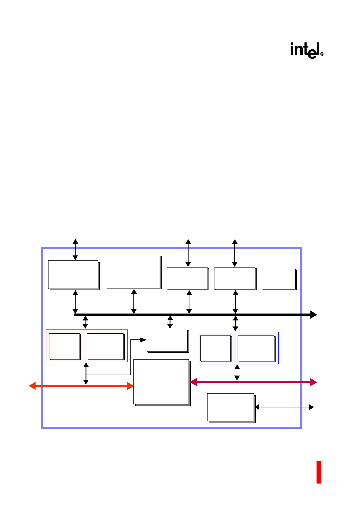
As indicated in Figure 1, the 80960Rx combines
many featur es with the 80960JF to crea te an intel ligent I/O processor. Subsections following the figure
briefl y descri be the ma in feat ures; for d etailed functional descriptions, refer to the
i960® RP Micropro-
cessor User’s Guide
(272736).
The PCI bus is an industry standard, high performanc e, low laten cy system bu s that ope rates up to
132 Mbyte/s. The 80960Rx, a multi-function PCI
device, is fully compliant with the
PCI Local Bus
Specification
Revisio n 2.1. Func tion 0 is the PCI -toPCI bridge unit; Function 1 is the ad dress translation
unit.
The PCI-to-PCI bridge unit is the connection path
between two independent 32-bit PCI buses and
provide s the ability to overcome PCI electri cal load
limits. The addition of the i960 core processor brings
intelligence to the bridge.
The 80960Rx, object code compatible with the i960
core processor, is capable of sustained execution at
the rate of one instruction per clock.
The local bus, a 32-bit multiplexed burst bus, is a
high-speed in terface to sys tem memory and I/O. A
full complement of control signals simplifies the
connection of the 80960Rx to external components.
Physical and logical memory attributes are
programmed via memory-mapped control registers
(MMRs), an extension not found on the i960 Kx, Sx
or Cx p roces sors . P hysi cal and l ogic al co nfig ura tion
registers enable the processor to operate with all
combinations of bus width and data object alignment.
Figure 1. i960
®
Rx I/O Processor at 3.3 V Functional Block Diagram
PCI-to-PCI
Bridge Unit
i960
®
JF
Core
Processor
Secondary
PCI Arbitration
Unit
Secondary PCI Bus
Primary PCI Bus
Local Memory
I2C Bus
Interface Unit
Memory
Controller
Internal
Arbitration
I2C Serial Bus
I/O APIC Bus
Interface Unit
I/O APIC Bus
Address
Translation
Unit
Two DMA
Channels
Address
Translation
Unit
One DMA
Channel
Message
Unit
Local Bus
Primary ATU
Secondary ATU

i960® Rx I/O Processor at 3.3 V
ADVANCE INFORMATION 3
2.1 Key Functional Units
2.1.1 PCI-to-PCI Bridge Unit
The PCI-to-PCI bridge unit (referred to as “bridge”)
connects two independent PCI buses. It is fully
compliant with the
PCI-to-PCI Bridge Architecture
Specification
Revision 1.0 published by the PCI
Special Interest Group. It allows certain bus transactions on one PCI bus t o be forwarde d to the other
PCI bus. Dedicated data queues support high performance bandwidth on the PCI buses. The i960
®
Rx
I/O Processor at 3.3 V supports PCI 64-bit Dual
Address Cycle (DAC) addressing.
The bridge has dedicated PCI configuration space
that is accessible through the primary PCI bus.
2.1.2 Private PCI Device Support
A key design feature is that the 80960Rx explicitly
suppor ts pri vate PCI de vices on the s econd ary PCI
bus without being detected by PCI configuration software. T he bridg e a nd Address T ran slatio n U n it work
togethe r to hide priv ate d evic es fr om P CI co nf igura tion cycles and allow these devices to use a private
PCI address space. The Address Translation Unit
uses normal PCI configuration cycles to configure
these devices.
2.1.3 DMA Controller
The DMA Controller supports low-latency, highthroughput data transfers between PCI bus agents
and 80960 local memory. Three separate DMA
channels accommodate data transfers: two for
primary PCI bus, one for the secondary PCI bus.
The DMA Controller supports chaining and
unaligned data transfers. It is programmable only
through the i960 core processor.
2.1.4 Address Translation Unit
The Address Translation Unit (ATU) allows PCI
transactions direct access to the 80960Rx local
memor y. Th e 80 96 0Rx ha s di rec t acce ss t o bo th P CI
buses. The ATU supports transactions between PCI
address space and 80960Rx addr ess space.
Address translation is controlled through programmable r egister s accessib le from bot h the PCI in terface a nd the 8096 0 core. Dual access to regi sters
allows flexibility in mapping the two address spaces.
2.1.5 Messaging Unit
The Messaging Unit (MU) provides data transfer
between the PCI system and the 80960Rx. It uses
interrupts to notify each system when new data
arrives. The MU has four messaging mechanisms.
Each allows a host processor or external PCI device
and the 80960Rx to communicate through message
passing and interrupt generation. The four mechanisms are Message Registers, Doorbell Registers,
Circular Queues, and Index Registers.
2.1.6 Memory Controller
The Memory Controller allows direct control of
externa l memo ry syst ems, incl uding D RAM, SR AM,
ROM and Fl a sh Mem or y. It pr ov ides a dir ec t co nnect
interface to memory that typically does not require
external logic. It features programmable chip selects,
a wait state generator and byte parity. External
memory can be configured as PCI addressable
memory or priv ate processor memory.
2.1.7 I
2
C Bus Interface Unit
The I
2
C (Inter-Inte grated Circuit) Bus Inter face Unit
allows the 80960 core to serve as a master and
slave device residing on the I
2
C bus. The I2C bus is
a serial bus developed by Philips Semiconductor
consi sting of a tw o pin in terfa ce. Th e bus allow s the
80960Rx to interface to other I
2
C peripherals and
microc ontrollers fo r system m anagemen t functions.
It requires a min imum of hardwa re for an economical
syste m to rel ay status and relia bility in formatio n on
the I/O sub system to an external device. For more
information, see
I2C Perip he rals for Micr ocon tro llers
(Philips Semiconductor)
2.1.8 I/O APIC Bus Interface Unit
The I/O APIC Bus Interface Unit provides an interface to the three-wire Advanced Programmable
Interrupt Con troller (APIC) bus that allows I/O API C
emulation in software. Interrupt messages can be
sent on the bus and EOI messages can be received.
4 ADVANCE INFORMATION
i960® Rx I/O Processor at 3.3 V
2.1.9 Secondary PCI Arbitration Unit
The Secondary PCI Arbitration Unit provides PCI
arbitration for the secondary PCI bus. It includes a
fairness algorithm with programmable priorities and
six PCI Request and Grant signal pairs. This arbitration unit can also be disabled to allow for external
arbitration.
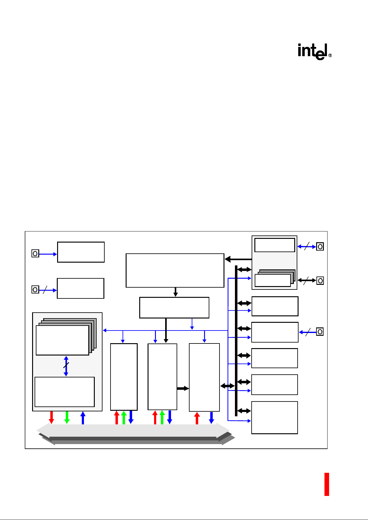
2.2 i960 Core Features (80960JF)
The processing power of the 80960Rx comes from
the 80960J F pro c es sor core. The 80 96 0J F i s a n ew ,
scalar implementation of the 80960 Core Architecture. Figure 2 shows a block diagram of the 80960JF
Core processor.
Factors that contribute to the 80960 family core’s
per form a n c e in cl ud e:
• Single-clock execution of most instructions
• Independent Multiply/Divide Unit
• Efficient instruction pipeline minimizes pipeline
break latenc y
• Register and resource scoreboarding allow
overlapped instruction execution
• 128-bit regi ster bus speeds local regi ster caching
• 4 Kbyte two-wa y set-associati v e, integrated
inst ruc tion cac he
• 2 Kbyte direct-mapped, integrated data cache
• 1 Kbyte integrated data RAM delivers zero w ait
state program data
The 80960 core operates out of its own 32-bit
address space, which is independent of the PCI
address space. The local bus memory can be:
• Made visible to the PCI address space
• Kept private to the 80960 core
• Allocated as a combination of the two
Figure 2. 80960JF Core Block Diag ram
Programmable
Bus
Control Unit
Interrupt Controller
Control
Address/
Instruction Sequencer
Physical Region
Configuration
Interrupt
Port
1K byte
Data RAM
Memory
Interface
Execution
Multiply
Unit
Divide
Unit
Memory-Mapped
Register Interface
Data Bus
Global / Local
Register File
SRC2 DSTSRC1
Address
Control
Effective
Constants
Generation
Unit
Address
32-bit Addr
32-bit Data
Bus Request
Queues
and
Two 32-Bit
Timers
8-Set
Local Register
SRC1
SRC2
DST
PLL, Clocks,
Power Mgmt
Boundary Scan
Controller
TAP
5
128
SRC1
SRC2
DST
SRC1
DST
9
32
32-bit buses
address / data
3 Independent 32-Bit SRC1, SRC2, and DST Buses
Instruction Cache
4 Kbyte Two-Way Set Associative
2Kbyte
Direct Mapped
Data Cache
S_CLK
Cache

i960® Rx I/O Processor at 3.3 V
ADVANCE INFORMATION 5
2.2.1 Burst Bu s
A 32-bit high-performance bus controller interfaces
the 80960Rx to external memory and peripherals.
The Bus Control Unit fetches instructions and transfers data on the l ocal bus at the r ate of up to four 32bit words per six clock cycles. The external
addre s s/d a ta bus is mul tip le xed.
Users may configure the 80960R x’s bus controller to
match an ap plic at ion’s fund ame ntal mem ory orga nization. Physi cal bus width is programmable for up to
eight re gion s. Data c aching is prog rammed through
a group of logica l memor y templa tes and a d efaults
register. The Bus Control Unit’s featur es include:
• Multiplexed external bus minimizes pin count
• 32-, 16- and 8-bit bus widths simplify I/O interfaces
• External ready control for address-to-data, data-todata and data-to-next-address wait state types
• Litt le endi an byte ordering
• Unaligned bus accesses performed transparently
• Three-deep load/store queue decouples the bus
from the 8096 0 core
Upon reset, th e 80960Rx conducts an i nternal self
test. Before executing its first instruction, it performs
an external bus confidence test by performing a
check su m on th e fir s t w or d s o f the In iti al iz at ion B o ot
Record.
2.2.2 Timer Unit
The tim er unit (TU ) con tains t wo in depe nden t 3 2-bit
timers that are capable of counting at several clock
rates and generating interr upts. Each is programme d
by use of the Timer Unit registers. These memorymapped registers are addressable on 32-bit boundaries. The timers have a single-shot mode and autoreload capabilities for continuous operation. Each
timer has an independent interrupt request to the
80960Rx’s interrupt controller. The TU can generate
a fault when unauthorized writes from user mode are
detected.
2.2.3 Priority Interrupt Controller
Low interrupt laten cy is criti cal to many embedded
applications. As part of its highly flexible interrupt
mechanism, the 80960Rx exploits several techniques to minimize latency:
• Inte rrupt vec tor s and int errup t hand ler ro utine s can
be reserved on-chip
• Register frames for high-priority interrupt handlers
can be cached on-chip
• The in terrupt stack can be plac ed in cacheable
memory space
2.2.4 Faults and Debugging
The 80960Rx employs a comprehensive fault model.
The pro cessor respon ds to faul ts by mak ing imp licit
calls to a fa ult h andl ing r outin e. Spec ific info rmati on
collected for each fault allows the fault handler to
diagno se exceptions an d rec ov e r appr op r ia tel y.
The processor also has built-in debug capabilities.
Via software, the 80960Rx may be configured to
detect as many as seven differ ent trace event types.
Alternatively, mark and fmark instructions can
generate trace events explicitly in the instruction
stream. Hardware breakpoint registers are also
available to trap on execution and data addresses.
2.2.5 On-Chip Cache and Data RAM
Memory subsystems often impose substantial wait
state penalties. The 80960Rx integrates considerable storage resources on-chip to decouple CPU
execution from the external b us. It also includes a
4 Kbyte instruction cache, a 2 Kbyte data cache and
1 Kbyte data RAM.
2.2.6 Local Register Cache
The 809 60 R x rap id ly allocates and deal loc a tes l oc al
register sets during context switches. The processor
needs to flush a register set to the stack only when it
saves more than seven sets to its local register
cache.
2.2.7 Test Features
The 80960Rx incorporates numerous features that
enhance the user’s ability to test both the processor
and the system to which it is attached. These
features include ONCE (On-Circuit Emulation) mode
and Boundary Scan (JTAG).
The 80960Rx provides testability features compatible with IEEE Standard Test Access Port and
Boundary Scan Architecture (IEEE Std. 1149.1).

i960® Rx I/O Processor at 3.3 V
6
ADVANCE INFORMATION
One of the boundary scan instructions, HIGHZ,
forces the processor to float all its output pins
(ONCE mode). ONCE mode can also be initiated at
reset without using the boundary scan mechanism.
ONCE mode is useful for board-level testing. This
feature allows a mounted 80960Rx to electrically
“remove” itself from a circuit board. This mode allows
system-level testing where a remote tester can
exercise the processor system.
The test logic does not interfere with component or
system behavior and ensures that components
function correctly, and also the connections between
variou s components are corr ect.
The JTAG Boundary Scan feature is an alternative
to conventional “bed-of-nails” testing. It can examine
conn ection s that mig ht otherw ise be inaccess ible to
a test sys tem.
2.2.8 Memory-Mapped Control Registers
The 80960Rx is compliant with 80960 family architecture and has the added advantage of memorymapp ed, intern al contro l registe rs not fo und on th e
80960K x, Sx or C x pro c es sors . T hi s fe atur e prov id es
software an interface to easily read and modify
internal control registers.
Each memory-mapped, 32-bit register is accessed
via regular memory-format instructions. The
processor ensures that these accesses do not
generate external bu s cycles.
2.2.9 Instructions, Data Types and Memory
Addressing Modes
As with all 80960 family processors, the 80960Rx
instru ction set suppor ts several different d ata types
and formats:
•Bit
• Bit fields
• I nt eg er (8-, 16-, 32-, 64-b it )
• Ordinal (8-, 16-, 32-, 64-bit unsigned integers)
• Tripl e word (96 bits)
• Quad word (128 bits)
The 80960Rx provides a full set of addressing
modes for C and assembly:
• Two Absolute modes
• Five Register Indire ct modes
• Index with displacement mode
• IP with displacement mode
Table 2 shows the available instructions.

i960® Rx I/O P rocessor at 3.3 V
ADVANCE INFORMATION 7
Table 2. 80960Rx Instruction Set
Data Movement Arithmetic Logical Bit, Bit Field and Byte
Load
Store
Move
Conditional Select
Load Address
Add
Subtract
Multiply
Divide
Remai nder
Modulo
Shift
Extended Shift
Exten de d Mu ltiply
Extended Divide
Add with Carry
Subtract with Carry
Condi tio na l A dd
Condi tio nal Subtr a ct
Rotate
And
Not And
And Not
Or
Exclusive Or
Not Or
Or Not
Nor
Exclusive Nor
Not
Nand
Set Bit
Clear Bit
Not Bit
Alter Bit
Scan For Bit
Span Over Bit
Extract
Modify
Scan Byte for Equal
Byte Swap
Comparison Branch Call/Return Fault
Compare
Conditional Compare
Compare and
Increment
Compare and
Decrement
Test Condition Code
Check Bit
Unconditional Branch
Condi tio na l B ran c h
Compa re and Br anch
Call
Call Extended
Call System
Return
Branch and Link
Conditional Fault
Synch ron iz e Fa ults
Debug
Processor
Manage me nt
Atomic
Modify Trace Controls
Mark
Force Mark
Flush Local Registers
Modify Arithmetic
Controls
Modify Process
Controls
Halt
System Control
Cache Control
Interrupt Control
Atomic Add
Atom i c Mo di fy

i960® Rx I/O Processor at 3.3 V
8
ADVANCE INFORMATION
3.0 PACKAGE INFORMATION
3.1 Package Introduction
The 80960Rx is offered in a SuperBGA* Ball Grid
Array (HL-PBG A) pac kag e. This is a peri mete r array
package with four rows of ball connections in the
outer area of the package. See Figure 4, 352L HLPBGA Package Diagram (Bottom View) (pg. 22).
Section 3.1.1, Functional Signal Definitions
describes signal function; Section 3.1.2, 352-Lead
HL-PBGA Pack age defines the signal and ball loca-
tions.
3.1.1 Functional Signal Definitions
Table 3 pres ents t he legend for interpreting the Type
Field in th e foll owi ng ta bles . Table 4 defines signals
associated with the bus interface. Table 5 defines
signals associated with basic control and test functions. Table 6 defines signals associated with the
Interrupt Unit. Table 7 define s PCI signa ls. Table 8
defin es Memo ry Contro ller sign als. Table 9 defines
DMA, APIC and I
2
C sign als. Tabl e 10 defin es cloc k
sign als. Table 11 defines ICE signals.
Table 3. Signal Type Definition
Symbol Description
I Input signal only.
O Output signal only.
I/O Signal can be either an input or out put.
OD Open Drain signal.
– Signal must be connected as described.
S (...) Synchronous. Inputs must meet setup
and hold times relative to S_CLK.
S(E) Edge sensitive input
S(L) Level sensitive input
A (...) Asynchronous. Inputs may be
asynchronous relative to S_CLK.
A(E) Edge sensitive input
A(L) Level sensitive input
R (...) While the P_RST# signal is asserted,
the signal:
R(1) is driven to V
CC
R(0) is driven to V
SS
R(Q) is a valid output
R(Z) Floats
R(H) is pulled up to V
CC
R(X) is driven to an unknown state
H (...) While the 80960Rx is in the hold state,
the signal:
H(1) is driven to V
CC
H(0) is driven to V
SS
H(Q) Maintains previous state or
continues to be a valid output
H(Z) Floats
P (...) While the 80960Rx is halted, the signal:
P(1) is driven to V
CC
P(0) is driven to V
SS
P(Q) Maintains previous state or
continues to be a valid output
K (...) While the Secondary PCI Bus is being
parked, the signal:
K(Z) Floats
K(Q) Maintains previous state or
continues to be a valid output

i960® Rx I/O P rocessor at 3.3 V
ADVANCE INFORMATION 9
Table 4. Signal Descriptions (Sheet 1 of 5)
NAME TYPE DESCRIPTION
AD31:0 I/O
S(L)
R(Z)
H(Z)
P(Q)
ADDRESS / DATA BUS carries 3 2-bit physic al addresses and 8-, 16- or 32bit data to and from memory. During an address (
T
a
) cycle, bits 2-31 contain
a physical word address (bits 0- 1 indicate SIZE; see below). During a data
(T
d
) cycle, read or write data is present on one or more contiguous bytes,
comprising A D31:24, AD23:1 6, AD15:8 and AD 7:0. Du ring write operation s,
unused signals are driven to determinate values.
SIZE, which comprises bits 0-1 of the AD lines dur ing a
T
a
cycle, specifies
the number of da ta transfers du ring the bus tra nsaction on the local bus.
When the DMA or ATUs initiate data transfers, transfer size shown below is
not valid.
AD1 AD0 Bus Transfers
0 0 1 Tran sfer
0 1 2 Tran sfers
1 0 3 Tran sfers
1 1 4 Transfers
When the 80960Rx enters Halt mode and the previous bus opera tion was:
• write — AD31:2 are driven with the last data value on the AD bus.
• read — AD31:2 are driven with the last address value on the AD bus.
Typically, AD1:0 reflect the SIZE i nformation of t he last bus transaction
(either instruction fetch or load/store) that was executed before entering Halt
mode.
ADS# O
R(1)
H(Z)
P(1)
ADDRESS STROBE indicate s a valid address and the start of a n ew bus
access. The processor asserts ADS# for the entire
T
a
cycle. External bus
contr ol logic typically samples ADS# at the end of the cycle.
ALE O
R(0)
H(Z)
P(0)
ADDRESS LATCH ENABLE indicates the transfer of a physical address.
ALE is asserted during a
T
a
cycle and deasserted before the beginning of the
T
d
state. It is active HIGH and floats to a high impedance state during a hold
cycle (T
h
).
BLAST# O
H(Z)
P(1)
BURST LAST indicates the last transfer in a bus access. B LAST# is
asserted in the last data transfer of burst and non-burst accesses. BLAST#
remains active while wait states are detected via the LRDYRCV# or
RDYRCV# signal on the memory controller. BLAST# becomes inactive after
the final data transfer in a bus cycle. BLAST# has a weak internal pullup
which is act ive dur ing res et to en sure normal ope ration when the signal is
not co nnect ed.
0 = Last Data Transfer
1 = Not the Last Data Transfer

i960® Rx I/O Processor at 3.3 V
10
ADVANCE INFORMATION
BE3:0# O
R(1)
H(Z)
P(1)
BYTE ENABLES select which of up to four data bytes on the bus participate
in the current bus access. Byte enable encoding depe nds on the bus widt h
of the memory region accessed:
32-bit bus:
BE3# en ab le s data on AD3 1: 24
BE2# en ab le s data on AD2 3: 16
BE1# en ab le s data on AD1 5: 8
BE0# en ab le s data on AD7 :0
16-bit bus:
BE3# becomes By te High Enable (enabl es data o n AD15:8)
BE2# is not used (state is high)
BE1# becomes Address Bit 1 (A1)
(increments with the assertion of LRDY# or RDYRCV#)
BE0# becomes By te Low En able (enables data on AD7:0)
8-bit bus:
BE3# is not used (state is high)
BE2# is not used (state is high)
BE1# becomes Address Bit 1 (A1)
(increments with the assertion of LRDY# or RDYRCV#)
BE0# becomes Address Bit 0 (A0)
(increments with the assertion of LRDY# or RDYRCV#)
The processor asserts byte enables, byte high enable and byte low enable
during
T
a
. Since unaligned bus r equests are split into separate bus transac-
tions, these signals do not toggle during a burst (32-bit bus only) from the
i960 core processor; they do toggle for DMA and ATU cycles. They remain
active through the last T
d
cycle.
DEN# O
H(Z)
P(1)
DATA ENABLE indicates data transfer cycles during a bus access. DEN# is
asserted at the start of the first data cycle in a bus access and deasserted at
the en d o f the l a st da ta cycle . DEN # is us ed w ith D T/ R # to pr ov ide c on tr ol f o r
data transceivers connected to the data bus. DEN# has a weak internal
pullup which is active during reset to ensure norm al operation when the
sig nal is not connected.
0 = Data Cycle
1 = Not a Data Cycle
Table 4. Signal Descriptions (Sheet 2 of 5)
NAME TYPE DESCRIPTION

i960® Rx I/O P rocessor at 3.3 V
ADVANCE INFORMATION 11
D/C#/
RST_MODE#
I/O
R(H)
H(Z)
P(Q)
DATA/CODE/RESET_MODE indicates that a bus access is a data access
or an instruction access. D/C# has the same timing as W/R#.
0 = Instruction Access
1 = Data Access
The RST_MODE# signal is sampled at Primary PCI bus reset to determine
whether the 80960 core is to be held in reset. When RST_MODE# is high,
the 80960Rx begins ini tialization immediately following the deassertion of
P_RST. When RST_MOD E is low, the 80960 core remains in re set until the
80960 core reset bit is cleared in the extended bridge contr ol register. This
signal has a weak internal pullup that is active during reset to ensure normal
operation when the signal is left unconnected.
0 = RST_MODE enab led
1 = RST_MODE not enabled
While the 80960 core is in reset, all peripherals may be accessed from th e
primary or sec ondary PCI buses depending on the status of the
WIDTH/HLTD1/RETRY/ signal.
DT/R# O
R(0)
H(Z)
P(Q)
DATA TRANSMIT / RECEIVE indicates the direction of data transfer to and
from the address/data bus. It is low during T
a
and Tw/Td cycles for a read; it
is high du r in g
T
a
and Tw/Td cycles for a write. DT/R # never changes state
when DEN# is asserted.
0 = Receive
1 = Tran smit
LOCK#/ONCE# I/O
S(L)
R(H)
H(Z)
P(Q)
BUS LOCK indica tes that an atomic read-modify-write operation is in
progress. The LOCK# output is asserted in the first clock of an atomic
operation and deasserted in the last data transfe r of the sequence. The
proce ss or does not grant HOLDA while ass e rting LOCK# . T hi s pre ve nt s
external agents from accessing memory involved in semaphore ope rations.
0 = Atomic Read-Modify- Write in Progress
1 = No Atomic Read-Modify-Write in Progress
ONCE MODE: The processor samples the ONCE input during reset. When
ONCE# is asser ted LOW at the end of reset, the processor enters O NCE
mode, stops all clocks and floats all output signals. LOCK#/ONCE# has a
weak internal pullup which is active during reset to ensure normal operation
when the signal is not connected.
0 = ONCE Mode Enabled
1 = ONCE Mode Not Enabled
LRDYRCV# O
R(1)
H(Q)
P(Q)
LOCAL READY/RECOVER, generat ed by th e 809 60 Rx’s memory controller
unit, is an output version of the READY/RECOVER (RDYRCV#) signal.
Refer to the RDYRCV# signal description.
Table 4. Signal Descriptions (Sheet 3 of 5)
NAME TYPE DESCRIPTION

i960® Rx I/O Processor at 3.3 V
12
ADVANCE INFORMATION
HOLD I
S(L)
HOLD is a re qu es t fro m an e xt ern al bu s mast er to ac qu ir e th e b us . When th e
processor receives HOLD and grants bus control to another master, it
asserts HOLDA , floats the address/data and control lines and enters the T
h
state. When HOLD is deasserted, the processor deasserts HOLDA and
enters either the T
i
or Ta state, resuming control of the address/data and
control lines. See Figure 32, HOLD/HOLDA Waveform For Bus Arbitration
(pg. 61).
0 = No Hold Request
1 = Hold Requested
HOLDA O
R(0)
H(1)
P(Q)
HOLD ACKNOWLEDGE indicates to an external bus master that the
processor has relinquished bus control. The processor can grant HOLD
requests and enter the T
h
state and while halted as well as during regular
operation. See Figure 32, HOLD /HOLDA Waveform For Bus Arbitration ( pg.
61).
0 = No Hold Acknowledged
1 = Hold Acknowledged
RDYRCV# I
S(L)
READY/RECOVER is only us ed in systems that use an external memory
con tro ll er ( a nd do no t u se th e 8 09 60 Rx’s memory controller unit). This signal
indicates that data on AD lines can be sampled or removed. When
RDYRC V# i s n ot as sert ed du rin g a T
d
cycle, th e Td cycle extends to the next
cycle by inserting a wait state (T
w
).
0 = Sample Data
1 = Do Not Sample Data
RDYRCV# has an alter nate function durin g the recovery (T
r
) state. The
processor co ntinues to insert recover y states until it samples the signal
HIGH. This gives slow external devices more time to float their buffers
before the processor drives addresses.
0 = Insert Wait States
1 = Recovery Complete
When using the internal memory controller, conn ect thi s signal to V
CC
through a 2.7 KΩ resistor.
W/R# O
R(0)
H(Z)
P(Q)
WRITE/READ specifies during a
T
a
cycle whether the operation is a write or
read. It is latched on-chip and remains valid during T
d
cycles.
0 = Read
1 = Write
WIDTH/
HLTD0
I/O
R(H)
H(Z)
P(Q)
WIDTH denotes the physical memory attributes for a bus transaction in
conjunction with WIDTH/HLTD1/RETRY:
WIDTH/HLTD1/RETRY WIDTH/HLTD0
0 0 8 Bits Wide
0 1 16 Bits Wide
1 0 32 Bits Wide
1 1 Undefined
WIDTH/HLTD0 For proper operation, do not connect this signal to ground.
This signal has a weak internal pullup which is active during reset to ensure
normal operation.
HLTD0 signal name has no function in the 80960Rx; the signal name is
included for 80960JF nami ng convention compatibility.
Table 4. Signal Descriptions (Sheet 4 of 5)
NAME TYPE DESCRIPTION

i960® Rx I/O P rocessor at 3.3 V
ADVANCE INFORMATION 13
WIDTH/
HLTD1/
RETRY
I/O
R(H)
H(Z)
P(Q)
WIDTH denotes the physical memory attributes for a bus tr ansact ion in
conjunction with the WIDTH/HLTD0 signal. Refer to description above.
RETRY is sampled at Primary PCI bus reset to determine when the Primary
PCI interface is disabled. When hi gh, the Primary PCI interface d isables PC I
config ur at io n cy cl es b y s igna li ng a RE TRY u ntil t he Ex tend ed B rid ge Co nt rol
Register’s Configuration Cycle Disable bit is cleared. When low, the Primary
PCI interface allows configurat ion cycles to occur. WIDTH/HLTD1/RETR Y
has a wea k internal pullup whic h is active during reset t o ensure normal
operation when the signal is not connected.
HLTD1 signal name has no function in the 80960Rx; the signal name is
included for 80960JF naming convention compatibility.
Table 5. Power Requirement, Processor Control and Test Signal Descriptions (Sheet 1 of 2)
NAME TYPE DESCRIPTION
FAIL# O
R(0)
H(Q)
FAIL indicates a failure of the processor’s built-in self-test performed during initialization. FAIL# is asserted immediately upon reset and toggles during self-test to
indicate the status of individual tests:
• When self-test passes, the processor deasserts F AIL# and commences operation
from user code.
• When self-test fails, the proces sor asserts FAI L# and th en stop s executi ng. Selftest failing does not caus e the bridge to stop exec ution.
0 = Self Test Failed
1 = Self Test Passed
L_RST# O LOCAL BUS RESET notifies external devices that the local bus has reset.
STEST I
S(L)
SELF TEST enables or disables the processor’s internal self-test feature at initialization. STEST is examined at the end of P_RST#. When STEST is asserted, the
processor performs its internal self-test and the external bus confidence test. When
STEST is deasserted, the processor performs only the external bus confidence test.
0 = Self Test Disabled
1 = Self Test Enabled
TCK I TEST CLOCK is a CPU input that provides the clocking function for IEEE 1149.1
Boundary Scan Testing (JTAG). State information and data ar e clocked into the
processor on the rising edge; data is clocked out of the processor on the falling edge.
TDI I
S(L)
TEST DATA INPUT is the serial input signal for JTAG. TDI is sampled on the rising
edge of TCK, during the SHIFT-IR and SHIFT-DR states of the Test Access Port.
This signal has a weak internal pullup whi c h is active during rese t to ensure normal
operation when the signal is not connected.
TDO O
R(Q)
H(Q)
P(Q)
TEST DATA OUTPUT is the serial output signal for JTAG. TDO is driven on the
falling edge of TCK during the SHIFT-IR and SHIFT-DR states of the Test Access
Port. At other times, TDO floats.
TMS I
S(L)
TEST MODE SELECT is sampled at the rising edge of TCK to select the operation of
the test logic for IEEE 1149.1 Boundary Scan testing. This signal has a weak internal
pullup which is active during reset to ensure norm al operation when the signal is not
connected.
Table 4. Signal Descriptions (Sheet 5 of 5)
NAME TYPE DESCRIPTION
i960® Rx I/O Processor at 3.3 V
14
ADVANCE INFORMATION
TRST# I
A(L)
TEST RESET asynchronously resets the Test Access Port (TAP) controller function
of IEEE1149.1 Boundary Scan testing (JTAG ). When using the Boundary Scan
feature, connect a pulldown resistor (1.5 KΩ) between this signal and V
SS
. Whe n
TAP is not used , this si gnal mu st be connected t o V
SS
; however, no resistor is
required. The signal has a weak internal pullup which must be overcome during reset
to ensure normal operation.
VCC – POWER. Connect to a 3.3 Volt V
CC
board plane.
VCC5 – 5 VOLT REFERENCE VOLTAGE. Input is the referen c e voltage for the 5 V-tolerant
I/O buffers. Connect this signal to +5 V for use with signals which exceed 3.3 V.
When all inputs are from 3.3 V components, connect this signal to 3.3 V.
VSS – GROUND. Connect to a V
SS
board plane.
N.C. – NO CONNECT. Do not make electrical connections to these balls.
VCCPLL3:1 I PLL POWER. For external connection to a 3.3 V V
CC
board plane. Power to PLLs
requires external filtering.
Table 6. Interrupt Unit Signal Descriptions
NAME TYPE DESCRIPTIO N
NMI# I
A(L)
NON-MASKABLE INTERRUPT causes a non-maskable interrupt event to occur.
NMI# is the highest priorit y inte rrupt source an d is level-det ect. When NMI# is
unused, it is recomm ended th at you connect it to V
CC
.
S_INT[A:D]#/
XINT3:0#
I
A(L)
SECONDARY PCI BUS INTERRUPT
1
requests an interrupt. S_INTx# assertion
and deassertion is asynchronous to S_CLK. A device asserts S_INTx# when
requesting attention from its device driver. When S_INTx# is asserted, it remains
asserted until the device driver clears the pending request. S_INTx# Interr upts
are level sensitive.
EXTERNAL INTERRUPT. Ext ern al devi ces us e t h is sign al t o re qu est a n in te rr up t
service. These signals operate in dedicated mode, where each signal is assigned
a dedicated interrupt level.
The S_INT[A:D]#/XINT3:0# signals can be directed as follows:
Sec. PCI Primary PCI 80960 Core Processor
S_INTA#
⇒ P_INTA# or XINT0#
S_INTB#
⇒ P_INTB# or XINT1#
S_INTC#
⇒ P_INTC# or XINT2#
S_INTD#
⇒ P_INTD# or XINT3#
XINT7:4# I
A(L)
EXTERNAL INTERRUPT. Ext ern al devi ces us e t h is sign al t o re qu est a n in te rr up t
service. These signals operate in dedicated mode, where each signal is assigned
a dedicated interrupt level.
NOTE:
1. PCI signal functions are summarized in this data sheet; refer to the
PCI Local Bus Specification
Revision
2.1 for a more complete definition .
Table 5. Power Requirement, Processor Control and Test Signal Descriptions (Sheet 2 of 2)
NAME TYPE DESCRIPTION

i960® Rx I/O P rocessor at 3.3 V
ADVANCE INFORMATION 15
Table 7. PCI Signal Descriptions (Sheet 1 of 3)
NAME TYPE DESCRIPTION
1
P_AD31:0 I/O
K(Q)
R(Z)
PRIMARY PCI ADDRESS/DATA is the primary multiplexed PCI address
and data bus.
P_C/BE3:0# I/O
K(Q)
R(Z)
PRIMARY PCI BUS COMMAND and BYTE ENABLE signals are
multiplexed on the same PCI signals. During an address phase,
P_C/BE3:0# define the bus command. During a data phase, P_C/BE3:0#
are used as byte enabl es.
P_DEVSEL# I/O
R(Z)
PRIMARY PCI BUS DEVICE SELECT is driven by a target agent that has
succe ssfully decoded the add ress. As an input, it indicates whether or not
an agent has been selected.
P_FRAME# I/O
R(Z)
PRIMARY PCI BUS CYCLE FRAME is asserted to indicate the beginning
and duration of an access on th e Primar y PCI bus.
P_GNT# I
R(Z)
PRIMARY PCI BUS GRANT indicates to the agent that access to the bus
has been granted. This is a point-to-point signal.
P_IDSEL I
S(L)
PRIMARY PCI BUS INITIALIZATION DEVICE SELECT selects the
80960Rx durin g a Configurat ion Read or Write command on the primary
PCI b us.
P_INT[A:D]# O
OD
R(Z)
PRIMARY PCI BUS INTERRUPT requests an interrupt. The assertion and
deassertion o f P_INTx# is asynchronous to S_CLK. A device a sserts its
P_INTx# line when requesting attention from its device driver. Once the
P_INTx# signal is asserted, it remains asserted until the device driver
clears the pending request. P_INTx# Interrupts are level sensitive.
P_IRDY# I/O
R(Z)
PRIMARY PCI BUS INITIATOR READY indicates the initiating agent’s
(bus master’s) ability to complete the current data phase of the transaction.
P_LOCK# I
S(L)
PRIMARY PCI BUS LOCK indicates an atomic operation that may require
multiple transactions to complete.
P_PAR I/O
K(Q)
R(Z)
PRIMARY PCI BUS PARITY. This signal ensures even parity across
P_AD31:0 an d P_C /BE3:0. A ll PCI devi c es mus t pr o vi de a par it y si gn al.
P_PERR# I/O
R(Z)
PRIMARY PCI BUS PARITY ERROR is used for reporting data parity
errors during all PCI transa ctions except a special cy cle.
P_REQ# O
K(Q)
R(Z)
PRIMARY PCI BUS REQUEST indicates to the arbiter that this agent
desires use of the bus. This is a point to point signal.
NOTE:
1. PCI signal functions are summarized in this data sheet; refer to the
PCI Local Bus Specification
Revision
2.1 for a more complete definition.

i960® Rx I/O Processor at 3.3 V
16
ADVANCE INFORMATION
P_RST# I
A(L)
PRIMARY RESET brings 80960Rx to a consistent state. When P_RST# is
asserted:
• PCI output signals are driven to a known consistent state.
• PCI bus interface output signals are three-stated.
• open drain signals such as P_SERR# are floated.
• S_RST# asserts.
P_RST# may be asynchronous to S_CLK when asserted or deasserted.
Although asynchronous, deassertion must be guaranteed to be a clean,
bounce-free edge.
P_SERR# I/O
OD
R(Z)
PRIMARY PCI BUS SYSTEM ERROR reports address and data parity
errors on the specia l cycle co mmand, or any other system error where the
resu lt wou ld be catas tro phic.
P_STOP # I/O
R(Z)
PRIMARY PCI BUS STOP indicates that the current target is requesting
the master to stop the current transaction on the primary PCI bus.
P_TRDY# I/O
R(Z)
PRIMARY PCI BUS TARGET READY indicates the target agent's
(selected device's) ability to complete the current data phase of the transaction.
S_AD31:0 I/O
R(0)
SECONDARY PCI ADDRESS/DATA is the secondary multiplexed PCI
address and data bus. A bus transaction consists of an address phase
followed by one or more data phases.
S_C/BE3:0# I/O
R(0)
SECONDARY PCI BUS COMMAND and BYTE ENABLE signals are
multiplexed on the same PCI signals. During an address phase,
S_C/BE3:0# define the bus command. During a data phase, S_C/BE3:0#
are used as byte enables.
S_DEVSEL# I/O
R(Z)
SECONDARY PCI BUS DEVICE SELECT is driven by a target agent that
has successfully decoded the address. As an input, it indicates wheth er or
not an agent has been selected.
S_FRAME# I/O
R(Z)
SECONDARY PCI BUS CYCLE FRAME is asserted to indicate the
beginning and durat ion of an access on the Secondary PCI bus.
S_GNT0#/
S_REQ#
O
R(Z)
SECONDARY PCI BUS GRANT0 is a grant signal sent to device 0 on the
secondary PCI bus when the internal Secondary PCI Bus Arbiter is
enabled.
SECONDARY PCI BUS REQUEST is the request signal for the 80960Rx
when the arbiter is disabled.
S_GNT5:1# O
R(Q)
SECONDARY PCI BUS GRANT are grant signals sent to devices 1-5 on
the secondary PCI bus.
S_IDSEL I
S(L)
SECONDARY PCI BUS INITIALIZATION DEVICE SELECT selects the
80960Rx during a Configuration Read or Write command on the secondary
PCI bus.
S_IR DY# I/O
R(Z)
SECONDARY PCI BUS INITIATOR READY indicates the initiating agent's
(bus master's) ability to complete the current data phase of the transaction.
Table 7. PCI Signal Descriptions (Sheet 2 of 3)
NAME TYPE DESCRIPTION
1
NOTE:
1. PCI signal functions are summarized in this data sheet; refer to the
PCI Local Bus Specification
Revision
2.1 for a more complete definition.

i960® Rx I/O P rocessor at 3.3 V
ADVANCE INFORMATION 17
S_LOCK# I/O
R(Z)
SECONDARY PCI BUS LOCK indicates the need to perform an atomic
operation on the secondary PCI bus.
S_PAR I/O
R(0)
SECONDARY PCI BUS PARITY. This signal ensures even parity across
S_AD31:0 an d S_C /BE3:0. A ll PCI devi c es mus t pr o vi de a par it y si gn al.
S_PERR# I/O
R(Z)
SECONDARY PCI BUS PARITY ERROR is used for reporting data parity
errors during all PCI transa ctions except a special cy cle.
S_REQ0#/
S_GNT#
I SECONDARY PCI BUS REQUEST0 is a request signal from device 0 on
the secondary PCI bus when the intern al Secondary PCI Bus Arb iter is
enabled.
SECONDARY PCI BUS GRANT is the grant signal for the 80960Rx when
the arbiter is disabled.
S_RST# O
R(Q)
SECONDARY PCI BUS RESET is an output based on P_RST#. It brings
PCI-specific registers, sequencers, and signals to a consistent state. When
P_RST# is asserted, it causes S_RST# to assert, and:
• PCI output signals are driven to a known consistent st ate.
• PCI bus interf ace outp ut signals are three-stated .
• open drain signals such a s S_SERR# are floated.
S_RST# may be as ynchronous to S_C LK when assert ed or deasserted.
S_SERR# I/O
OD
R(Z)
SECONDARY PCI BUS SYSTEM ERROR repor ts address and data parity
errors on the special cycle command, or any other system error wh ere the
result would be catastrophic.
S_STOP# I/O
R(Z)
SECONDARY PCI BUS STOP indicates that the current target is
requesting t he master to sto p the current transaction on the secondary PCI
bus.
S_TRDY# I/O
R(Z)
SECONDARY PCI BUS TARGET READY indicates the target agent's
(selected device's) ability to complete the current data phase of the transaction.
S_REQ4:1# I
S(L)
SECONDARY PCI BUS REQUEST 4:1 are request signals from devices
1-4 on t he second ary PCI bus.
S_REQ5#/
S_ARB_EN
I
S(L)
SECONDARY PCI BUS REQUEST 5 is the request signal from device 5 on
the secondary P CI bus.
SECONDARY PCI BUS ARBITER ENABLE defines the power-up status
of the internal sec o ndary arbitration unit. A valid high at the deas sertion of
P_RST# enables the internal secondary arbiter. A valid low at the
deassertion of P_RST# disables the internal secondary arbiter .
Table 7. PCI Signal Descriptions (Sheet 3 of 3)
NAME TYPE DESCRIPTION
1
NOTE:
1. PCI signal functions are summarized in this data sheet; refer to the
PCI Local Bus Specification
Revision
2.1 for a more complete definition.

i960® Rx I/O Processor at 3.3 V
18
ADVANCE INFORMATION
Table 8. Memory Controller Signal Descriptions (She et 1 of 2)
NAME TYPE DESCRIPTION
CAS7:0# O
R(1)
H(Q)
P(Q)
COLUMN ADDRESS STROBE signals are used for DRAM accesses and are
asserted when the MA11:0 signals contain a valid column address. CAS7:0#
signals are asserted during refresh.
Non-Interleaved Operation:
CAS0#,CAS4# = BE 0# lane access
CAS1#,CAS5# = BE1# lane access
CAS2#,CAS6# = BE2# lane access
CAS3#,CAS7# = BE3# lane access
Interleave d Operation:
CAS0# = B E0# Even leaf lane access
CAS1# = B E1# Even leaf lane access
CAS2# = B E2# Even leaf lane access
CAS3# = B E3# Even leaf lane access
CAS4# = BE0# Odd leaf lane access
CAS5# = BE1# Odd leaf lane access
CAS6# = BE2# Odd leaf lane access
CAS7# = BE3# Odd leaf lane access
CE1:0# O
R(1)
H(Q)
P(Q)
CHIP ENABLE signals indicate an access to one of the t wo SRAM/ FLASH/
ROM memory banks. CE0# and CE1# are never asserted at the same time.
These signals are valid during the entire memory operation. CE0# is asserted
for accesses to memory bank 0. CE 1# is asserted for acc esses to memory
bank 1.
DALE1:0 O
R(0)
H(Q)
P(Q)
DRAM ADDRESS LATCH ENABLE signals support external address demultiplexing of the MA11:0 address lines for interleaved DRAM systems. Use
these t o dir ect ly int erf a ce t o ‘373 ’ t yp e l atch es . Th ese si gn al s ar e o nly vali d f o r
accesses to interleav ed memory systems. DALE0 is asserted during a valid
even lea f ad dr e ss . D ALE1 is asser te d du r in g a va lid odd leaf addres s.
DP3:0 I/O
R(X)
H(Q)
P(Q)
DATA PARITY carries the parity information for DRAM accesses. Each parity
bit corresponds to a group of 8 data bus signals as follow s:
DP0 — AD7:0 DP2 — AD23:16
DP1 — AD15:8 DP3 — AD31:24
The memory controller gener ates p arity information for local bus writes during
data cycles. During read data cycles, the memory contr oller checks parit y and
provides notification of parity errors on the clock following the data cycle.
Pari ty checking and polarity are user-programmable. Pa rity generation and
checking are valid only for data lines that have their associated enable bits
assert ed.
DWE1:0# O
R(1)
H(Q)
P(Q)
DRAM WRITE ENABLE signals dist i ngu i sh bet wee n r e ad an d w rit e acc ess es
to DRAM. DWE1:0# lines are asserted for writes and deasserted for reads.
CAS7:0# deter mine valid bytes lanes during the ac cess. These two outputs
are functionally equivalent for all DRAM accesses; these provide increased
drive capability for heavily loaded systems.
LEAF1:0# O
R(1)
H(Q)
P(Q)
LEAF ENABLE signals c on tro l th e d ata o ut put en ab le s of th e m emo ry sy st em
during an interleaved DRAM read acce ss. Use these t o directly interface to
either DRAM or transceiver output enable signals. LEAF0# is asserted during
an even leaf access. LEAF1# is asserted during an odd leaf access.

i960® Rx I/O P rocessor at 3.3 V
ADVANCE INFORMATION 19
MA11:0 O
R(X)
H(Q)
P(Q)
MULTIPLEXED ADDRESS signals are multi-purpose depending on the
device that is selected.
For me mory banks 0 and 1, these signals output address bits A13:2. These
address bits are incremented for each data transfer of a burst access.
For DR AM bank, these signals output the row/column multiplexed address
bits 11:0. The relationship betw een the AD31:0 lines and the MA11:0 lines
depends on the bank size, type and arrangement of the DRAM that is
accessed.
MWE3:0# O
R(1)
H(Q)
P(Q)
MEMORY WRITE ENABLE signals for write accesses to SRAM/FLASH
devices. The MWE’s rising edge strobes valid data into these devices.
MWE0# is asserted for writes to the BE0# lane
MWE1# is asserted for writes to the BE1# lane
MWE2# is asserted for writes to the BE2# lane
MWE3# is asserted for writes to the BE3# lane
RAS3:0# O
R(1)
H(Q)
P(Q)
ROW ADDRESS STROBE signals are used for DRAM accesses and are
asserted when the MA11:0 signals contain a valid row address. RAS3:0#
always deasserts after the last data transfer in a DRAM access.
Non-Interleaved Operation:
RAS0# = Bank0 ac cess
RAS1# = Bank1 ac cess
RAS2# = Bank2 ac cess
RAS3# = Bank3 ac cess
Interl ea ve d O pe r at ion :
RAS0,2# = Even leaf
RAS1,3# = Odd leaf
Table 9. DMA, APIC, I
2
C Units Signal Descriptions (She et 1 of 2)
NAME TYPE DESCRIPTION
DACK# O
R(1)
H(Q)
P(Q)
DMA DEMAND MODE ACKNOWLEDGE The DMA Controller asserts this
signal to indicate (1) it can receive new data from an external device or (2) it
has data to send to an external device.
DREQ# I
S(L)
DMA DEMAND MODE REQUEST External devices use this signal to indicate
(1) new data is ready for transfer to the DMA controller or (2) buffers are
available to receive data from the DMA controller.
PICCLK I APIC BUS CLOCK provides synchr onous o peration of the APIC bus.
PICD1:0 I/O
OD
R(Z)
H(Q)
P(Q)
APIC DATA lines comprise the data portion of the APIC 3-wire bus.
Table 8. Memory Controller Signal Descriptions (Sheet 2 of 2)
NAME TYPE DESCRIPTION

i960® Rx I/O Processor at 3.3 V
20
ADVANCE INFORMATION
SCL I/O
OD
R(Z)
H(Q)
P(Q)
I2C CLOCK provides synchronous I2C bus op eration .
SDA I/O
OD
R(Z)
H(Q)
P(Q)
I
2
C DATA used fo r data transfer and arbitration on the I2C bus.
WAIT# O
R(1)
H(Q)
P(Q)
WAIT is an output that allows the DMA controller to insert wait states during
DMA ac cesses to an exter nal mem ory system.
Table 10. Clock Signal
NAME TYPE DESCRIPTION
S_CLK I SYNCHRONOUS PCI BUS CLOCK Provides the processor’s fundamental time
base. All input/output ti mings are relative to S_CLK.
Table 11. ICE Signal Descriptions
NAME TYPE DESCRIPTION
ICEADS# O ICE ADDRESS/DATA STATUS indicates a valid address and the start of a new
bus access. ICEADS# is active for accesses to ext ernal microcode.
ICEBRK# I ICE BREAK forces th e processor to tr ansition from emulation to interrogation
mode.
ICEBUS7:0 I/O ICE BUS is a bidirectional 8-bit bus linking the processor and the emulator.
Used in various modes.
ICECLK O ICE CLOCK output si gnal to which all ICE bus signals are synchronized.
ICELOCK# I ICE LOCK is sampled during 80960 core reset to protect ICE configuration.
ICEMSG# I ICE MESSAGE signal used to acknowledge data from the processor to the
emulator. Us ed only during interrogation mode.
ICESEL# I ICESEL enables or disables the ICE unit.
ICEVLD# O ICE VALID indicates the processor is driving the ICEBUS with valid data.
MSGFRM# O ICE MESSAGE FRAME indicates that trace messages are being issued to the
ICEBUS. Used in emulation mode only.
Table 9. DMA, APIC, I
2
C Units Signal Descriptions (Sheet 2 of 2)
NAME TYPE DESCRIPTION

i960® Rx I/O P rocessor at 3.3 V
ADVANCE INFORMATION 21
3.1.2 352-Lead HL-PBGA Package
Figure 3. 352L HL-PBGA Package Diagram (Top and Side View)
NOTES:
1. All dimensions and tolerances conform to ANSI Y14.5M 1982.
2. All dimensions are in millimeters.
3. Tin/Lead mix: 63%/37%.
4. Pad plating method: Electrolytic.
5. Encapsulant size: 22.38 x 22.38 mm (max).
Body Size
Ball spacing is 1.27 mm
35 ± 0.10 mm
1.54
± 0.13
mm
35 ± 0.10
mm
Ball Footprint
31.75 mm
0.91 ± 0.06 mm
Package Height
0.63
± 0.07
mm
Ball width is 0.75 ± 0.15 mm
1.63 mm
Ball A1 Corner
i960
®
GC80960RxZ Z
FFFFFFFF SS
Q QQQQ
©
‘9x ‘9x
M
i

i960® Rx I/O Processor at 3.3 V
22
ADVANCE INFORMATION
Figu re 4. 352L HL-PBGA Packag e Diagram (Bottom View)
1
2
3
4
5
6
7
8
9
10
11
12
13
14
15
16
17
18
19
20
21
22
23
24
25
26
1
2
3
4
5
6
7
8
9
10
11
12
13
14
15
16
17
18
19
20
21
22
23
24
25
26
ABCDEFGHJKLMNPRTUVWYAA
AB
AC
AD
AE
AF
ABCDEFGHJKLMNPRTUVWYAA
AB
AC
AD
AE
AF

i960® Rx I/O Processor at 3.3 V
ADVANCE INFORMATION 23
Table 12. 352-Lead HL-P BGA Package — Signal Name Order (She et 1 of 4)
Signal Ball #
AD0 A18
AD1 B18
AD2 C17
AD3 A17
AD4 B17
AD5 C16
AD6 A16
AD7 B16
AD8 C15
AD9 A15
AD10 B15
AD11 C14
AD12 A14
AD13 B14
AD14 C13
AD15 A13
AD16 B13
AD17 C12
AD18 A12
AD19 B12
AD20 C11
AD21 A11
AD22 B11
AD23 C10
AD24 A10
AD25 B10
AD26 C9
AD27 A9
AD28 B9
AD29 C8
AD30 A8
AD31 B8
ADS# B21
ALE C20
BE0# A22
BE1# B22
BE2# C21
BE3# A21
BLAST# C23
CAS0# F1
CAS1# F2
CAS2# G3
CAS3# G1
CAS4# G2
CAS5# H3
CAS6# H1
CAS7# H2
CE0# L3
CE1# L1
D/C#/RST_MODE# AF4
DACK# AD3
DALE0 M1
DALE1 M2
DEN# A23
DP0 C2
DP1 D3
DP2 D1
DP3 D2
DREQ# AD2
DT/R# B23
DWE0# K1
DWE1# K2
FAIL# AD5
HOLD V1
HOLDA V3
ICEADS# AC1
ICEBRK# AA1
ICEBUS0 V2
ICEBUS1 W3
ICEBUS2 W1
ICEBUS3 W2
ICEBUS4 Y3
ICEBUS5 Y1
ICEBUS6 Y2
ICEBUS7 AA3
ICECLK AB2
ICELOCK# AB3
ICEMSG# AA2
Signal Ball #
ICESEL# AC2
ICEVLD# AB1
LEAF0 L2
LEAF1 M3
LOCK#/ONCE# AD4
LRDYRCV# C19
LRST# AD6
MA0 C7
MA1 A7
MA2 B7
MA3 C6
MA4 B6
MA5 C5
MA6 A5
MA7 B5
MA8 C4
MA9 B4
MA10 C3
MA11 B3
MSGFRM# AC3
MWE0# J3
MWE1# J1
MWE2# J2
MWE3# K3
NC A20
NC AE4
NC B20
NC C18
NMI# T3
P_AD0 AD24
P_AD1 AE23
P_AD2 AF23
P_AD3 AD23
P_AD4 AE22
P_AD5 AF22
P_AD6 AD22
P_AD7 AE21
P_AD8 AD21
P_AD9 AE20
Signal Ball #

i960® Rx I/O Processor at 3.3 V
24 ADVANCE INFORMATION
Table 12. 352-Lead HL-PBGA Package — Signal Name Order
(She et 2 of 4)
P_AD10 AF20
P_AD11 AD20
P_AD12 AE19
P_AD13 AF19
P_AD14 AD19
P_AD15 AE18
P_AD16 AE14
P_AD17 AF14
P_AD18 AD14
P_AD19 AE13
P_AD20 AF13
P_AD21 AD13
P_AD22 AE12
P_AD23 AF12
P_AD24 AF11
P_AD25 AD11
P_AD26 AE10
P_AD27 AF10
P_AD28 AD10
P_AD29 AE9
P_AD30 AF9
P_AD31 AD9
P_C/BE0# AF21
P_C/BE1# AF18
P_C/BE2# AD15
P_C/BE3# AE11
P_DEVSEL# AF16
P_FRAME# AF15
P_GNT# AF8
P_IDSEL AD12
P_INTA# AF6
P_INTB# AE6
P_INTC# AD7
P_INTD# AF 7
P_IRDY# AE15
P_LOCK# AD17
P_PAR AD18
P_PERR# AF17
P_REQ# AE8
Signal Ball #
P_RST# AE7
P_SERR# AE17
P_STOP# AE16
P_TRDY# AD16
PICCLK U3
PICD0 T1
PICD1 T2
RAS0# E3
RAS1# E1
RAS2# E2
RAS3# F3
RDYRCV# B19
S_AD0 AE24
S_AD1 AD25
S_AD2 AC24
S_AD3 AC26
S_AD4 AC25
S_AD5 AB24
S_AD6 AB26
S_AD7 AB25
S_AD8 AA26
S_AD9 AA25
S_AD10 Y24
S_AD11 Y26
S_AD12 Y25
S_AD13 W24
S_AD14 W26
S_AD15 W25
S_AD16 R25
S_AD17 P24
S_AD18 P26
S_AD19 P25
S_AD20 N24
S_AD21 N26
S_AD22 N25
S_AD23 M24
S_AD24 L24
S_AD25 L26
S_AD26 L25
Signal Ball #
S_AD27 K24
S_AD28 K26
S_AD29 K25
S_AD30 J24
S_AD31 J26
S_C/BE0# AA24
S_C/BE1# V24
S_C/BE2# R26
S_C/BE3# M25
S_CLK F25
S_DEVSEL# T24
S_FRAME# R24
S_GNT0#/S_REQ# H26
S_GNT1# G24
S_GNT2# G25
S_GNT3# F26
S_GNT4# E26
S_GNT5# D24
S_IDSEL M26
S_INTA#/XINT0# N1
S_INTB#/XINT1# N2
S_INTC#/XINT2# P3
S_INTD#/XINT3# P1
S_IRDY# T25
S_LOCK# U26
S_PAR V26
S_PERR# U24
S_REQ0#/S_GNT# H24
S_REQ1# H25
S_REQ2# G26
S_REQ3# F24
S_REQ4# E24
S_REQ5#/S_ARB_EN E25
S_RST# J25
S_SERR# V25
S_STOP# U25
S_TRDY# T26
SCL U1
SDA U2
Signal Ball #

i960® Rx I/O Processor at 3.3 V
ADVANCE INFORMATION 25
Table 12. 352-Lead HL-PBGA Package — Signal Name Order
(She et 3 of 4)
STEST AE3
TCK B24
TDI D26
TDO D25
TMS C24
TRST# C25
V
CC
A1
V
CC
A2
V
CC
A24
V
CC
A25
V
CC
A26
V
CC
AA23
V
CC
AB4
V
CC
AC6
V
CC
AC8
V
CC
AC10
V
CC
AC12
V
CC
AC14
V
CC
AC16
V
CC
AC18
V
CC
AC20
V
CC
AC22
V
CC
AD1
V
CC/VSS
(1) AD8
V
CC
AD26
V
CC
AE1
V
CC
AE2
V
CC
AE25
V
CC
AE26
V
CC
AF1
V
CC
AF2
V
CC
AF3
V
CC
AF24
V
CC
AF25
V
CC
AF26
V
CC
B1
V
CC
B2
Signal Ball #
V
CC
B25
V
CC
B26
V
CC
C1
V
CC
C26
V
CC
D5
V
CC
D7
V
CC
D9
V
CC
D11
V
CC
D13
V
CC
D15
V
CC
D17
V
CC
D19
V
CC
D21
V
CC
E23
V
CC
F4
V
CC
G23
V
CC
H4
V
CC
J23
V
CC
K4
V
CC
L23
V
CC
M4
V
CC
N23
V
CC
P4
V
CC
R23
V
CC
T4
V
CC
U23
V
CC
V4
V
CC
W23
V
CC
Y4
V
CC5
A3
VCCPLL1 A19
VCCPLL2 A6
VCCPLL3 A4
V
SS
AA4
V
SS
AB23
V
SS
AC4
V
SS
AC5
Signal Ball #
V
SS
AC7
V
SS
AC9
V
SS
AC11
V
SS
AC13
V
SS
AC15
V
SS
AC17
V
SS
AC19
V
SS
AC21
V
SS
AC23
V
SS
D4
V
SS
D6
V
SS
D8
V
SS
D10
V
SS
D12
V
SS
D14
V
SS
D16
V
SS
D18
V
SS
D20
V
SS
D22
V
SS
D23
V
SS
E4
V
SS
F23
V
SS
G4
V
SS
H23
V
SS
J4
V
SS
K23
V
SS
L4
V
SS
M23
V
SS
N4
V
SS
P23
V
SS
R4
V
SS
T23
V
SS
U4
V
SS
V23
V
SS
W4
V
SS
Y23
W/R# C22
Signal Ball #
NOTES:
1. Ball AD8 must be tied to either V
CC
or VSS.

i960® Rx I/O Processor at 3.3 V
26 ADVANCE INFORMATION
Table 12. 352-Lead HL-PBGA Package — Signal Name Order (She et 4 of 4)
WAIT# N3
WIDTH/HLTD0 AF5
WIDTH/HLTD1/RETRY AE5
Signal Ball #
XINT4# P2
XINT5# R3
XINT6# R1
Signal Ball #
XINT7# R2
Signal Ball #

i960® Rx I/O Processor at 3.3 V
ADVANCE INFORMATION 27
Table 13. 352-Lead HL-PBGA Pinout — Ballpad Number Order (Sheet 1 of 4)
Ball # Signal
A1 V
CC
A2 V
CC
A3 V
CC5
A4 VCCPLL3
A5 MA6
A6 VCCPLL2
A7 MA1
A8 AD30
A9 AD27
A10 AD24
A11 AD21
A12 AD18
A13 AD15
A14 AD12
A15 AD9
A16 AD6
A17 AD3
A18 AD0
A19 VCCPLL1
A20 NC
A21 BE3#
A22 BE0#
A23 DEN#
A24 V
CC
A25 V
CC
A26 V
CC
B1 V
CC
B2 V
CC
B3 MA11
B4 MA9
B5 MA7
B6 MA4
B7 MA2
B8 AD31
B9 AD28
B10 AD25
B11 AD22
B12 AD19
B13 AD16
B14 AD13
B15 AD10
B16 AD7
B17 AD4
B18 AD1
B19 RDYRCV#
B20 NC
B21 ADS#
B22 BE1#
B23 DT/R#
B24 TCK
B25 V
CC
B26 V
CC
C1 V
CC
C2 DP0
C3 MA10
C4 MA8
C5 MA5
C6 MA3
C7 MA0
C8 AD29
C9 AD26
C10 AD23
C11 AD20
C12 AD17
C13 AD14
C14 AD11
C15 AD8
C16 AD5
C17 AD2
C18 NC
Ball # Signal
C19 LRDYRCV#
C20 ALE
C21 BE2#
C22 W/R#
C23 BLAST#
C24 TMS
C25 TRST#
C26 V
CC
D1 DP2
D2 DP3
D3 DP1
D4 V
SS
D5 V
CC
D6 V
SS
D7 V
CC
D8 V
SS
D9 V
CC
D10 V
SS
D11 V
CC
D12 V
SS
D13 V
CC
D14 V
SS
D15 V
CC
D16 V
SS
D17 V
CC
D18 V
SS
D19 V
CC
D20 V
SS
D21 V
CC
D22 V
SS
D23 V
SS
D24 S_GNT5#
D25 TDO
D26 TDI
E1 RAS1#
Ball # Signal

i960® Rx I/O Processor at 3.3 V
28 ADVANCE INFORMATION
Table 13. 352-Lead HL-PBGA Pinout — Ballpad Number Order
(She et 2 of 4)
E2 RA S2#
E3 RA S0#
E4 V
SS
E23 V
CC
E24 S_REQ4#
E25 S_REQ5#/S_ARB_EN
E26 S_GN T4#
F1 CAS0#
F2 CAS1#
F3 RAS3#
F4 V
CC
F23 V
SS
F24 S_REQ3 #
F25 S_CLK
F26 S_ G NT3 #
G1 CAS3#
G2 CAS4#
G3 CAS2#
G4 V
SS
G23 V
CC
G24 S_ GN T1#
G25 S_ GN T2#
G26 S_REQ2 #
H1 CAS6#
H2 CAS7#
H3 CAS5#
H4 V
CC
H23 V
SS
H24 S_REQ0#/S_GNT#
H25 S_ REQ1 #
H26 S_GNT0#/S_REQ#
J1 MWE1#
J2 MWE2#
J3 MWE0#
J4 V
SS
Ball # Signal
J23 V
CC
J24 S_AD30
J25 S_RST#
J26 S_AD31
K1 DWE0#
K2 DWE1#
K3 MWE3#
K4 V
CC
K23 V
SS
K24 S_AD27
K25 S_AD29
K26 S_AD28
L1 CE1#
L2 LEA F0#
L3 CE0#
L4 V
SS
L23 V
CC
L24 S_ AD24
L25 S_ AD26
L26 S_ AD25
M1 DALE0
M2 DALE1
M3 LEA F 1 #
M4 V
CC
M23 V
SS
M24 S_AD23
M25 S_C/BE3#
M26 S_IDSEL
N1 S_INTA#/XINT0#
N2 S_INTB#/XINT1#
N3 WAIT#
N4 V
SS
N23 V
CC
N24 S_AD20
N25 S_AD22
Ball # Signal
N26 S_AD21
P1 S_INTD#/XINT3#
P2 XINT4#
P3 S_INTC#/XINT2#
P4 V
CC
P23 V
SS
P24 S_AD17
P25 S_AD19
P26 S_AD18
R1 XINT6#
R2 XINT7#
R3 XINT5#
R4 V
SS
R23 V
CC
R24 S_FRAME#
R25 S_AD16
R26 S_C/BE2#
T1 PICD0
T2 PICD1
T3 NMI#
T4 V
CC
T23 V
SS
T24 S_DEVSEL#
T25 S_IRDY#
T26 S_TRDY#
U1 SCL
U2 SDA
U3 PICCLK
U4 V
SS
U23 V
CC
U24 S_PERR#
U25 S_STOP#
U26 S_LOCK#
V1 HOLD
V2 ICEBUS0
Ball # Signal

i960® Rx I/O Processor at 3.3 V
ADVANCE INFORMATION 29
Table 13.
352-Lead HL-PBGA Pinout — Ballpad Number Order (She et 3 of 4)
V3 HOLDA
V4 V
CC
V23 V
SS
V24 S_C/BE1#
V25 S_SERR#
V26 S_PAR
W1 ICEBUS2
W2 ICEBUS3
W3 ICEBUS1
W4 V
SS
W23 V
CC
W24 S_AD13
W25 S_AD15
W26 S_AD14
Y1 ICEBUS5
Y2 ICEBUS6
Y3 ICEBUS4
Y4 V
CC
Y23 V
SS
Y24 S_AD10
Y25 S_AD12
Y26 S_AD11
AA1 ICEBRK#
AA2 ICEMSG#
AA3 ICEBUS7
AA4 V
SS
AA23 V
CC
AA24 S_C/BE0#
AA25 S_AD9
AA26 S_AD8
AB1 ICEVLD#
AB2 ICECLK
AB3 ICELOCK#
Ball # Signal
AB4 V
CC
AB23 V
SS
AB24 S_AD5
AB25 S_AD7
AB26 S_AD6
AC1 ICEADS#
AC2 ICESEL#
AC3 MSGFRM#
AC4 V
SS
AC5 V
SS
AC6 V
CC
AC7 V
SS
AC8 V
CC
AC9 V
SS
AC10 V
CC
AC11 V
SS
AC12 V
CC
AC13 V
SS
AC14 V
CC
AC15 V
SS
AC16 V
CC
AC17 V
SS
AC18 V
CC
AC19 V
SS
AC20 V
CC
AC21 V
SS
AC22 V
CC
AC23 V
SS
AC24 S_AD2
AC25 S_AD4
AC26 S_AD3
AD1 V
CC
AD2 DREQ#
Ball # Signal
AD3 DACK#
AD4 LOCK#/ONCE#
AD5 FAIL#
AD6 LRST#
AD7 P_INTC#
AD8 V
CC/VSS
(1)
AD9 P_AD31
AD10 P_AD28
AD11 P_AD25
AD12 P_IDSEL
AD13 P_AD21
AD14 P_AD18
AD15 P_C/BE2#
AD16 P_TRDY#
AD17 P_LOCK#
AD18 P_PAR
AD19 P_AD14
AD20 P_AD11
AD21 P_AD8
AD22 P_AD6
AD23 P_AD3
AD24 P_AD0
AD25 S_AD1
AD26 V
CC
AE1 V
CC
AE2 V
CC
AE3 STEST
AE4 NC
AE5 WIDTH/HLTD1/RETRY
AE6 P_INTB#
AE7 P_RST#
AE8 P_REQ#
AE9 P_AD29
Ball # Signal
NOTES:
1. Ball AD8 must be tied to either V
CC
or VSS.

i960® Rx I/O Processor at 3.3 V
30 ADVANCE INFORMATION
Table 13.
352-Lead HL-PBGA Pinout — Ballpad Number Order (She et 4 of 4)
AE10 P_AD26
AE11 P_C/BE3#
AE12 P_AD22
AE13 P_AD19
AE14 P_AD16
AE15 P_IRDY#
AE16 P_STOP#
AE17 P_SERR#
AE18 P_AD15
AE19 P_AD12
AE20 P_AD9
AE21 P_AD7
AE22 P_AD4
AE23 P_AD1
AE24 S_AD0
Ball # Signal
AE25 V
CC
AE26 V
CC
AF1 V
CC
AF2 V
CC
AF3 V
CC
AF4 D/C#/RST_MODE#
AF5 WIDTH/HLTD0
AF6 P_INTA#
AF7 P_INTD #
AF8 P_G NT#
AF9 P_ AD30
AF10 P_AD27
AF11 P_AD24
AF12 P_AD23
AF13 P_AD20
Ball # Signal
AF14 P_AD17
AF15 P_FRAME#
AF16 P_DEVSEL#
AF17 P_PERR#
AF18 P_C/BE1#
AF19 P_AD13
AF20 P_AD10
AF21 P_C/BE0#
AF22 P_ AD5
AF23 P_ AD2
AF24 V
CC
AF25 V
CC
AF26 V
CC
Ball # Signal

i960® Rx I/O Processor at 3.3 V
ADVANCE INFORMATION 31
3.2 Package Thermal Specifications
The dev ice is spe cifie d for op era tion when TC (case
temperature) is within the range of 0° C to 95° C.
Case temperature may be measured in any
envir onment t o determin e wheth er the p rocessor is
within specifie d operat ing range. Measure th e case
temperature at the center of the top surface,
opposite the ballpad.
3.2.1 Thermal Specifications
This section defines the terms used for thermal
analysis.
3.2.1.1 Am bient Temperature
Ambien t temperatu re, T
A
, is the temperatu re of the
ambient air surrounding the package. In a system
environment, ambient temperature is the temperature of the air upstream from the package.
3.2.1.2 Case Temperature
To ensu re functional ity and reliabi lity, the devi ce is
specified for proper operation when the case
temperature, T
C
, is within the specified range in
Table 16, Operating Conditions (pg. 34).
When measuring case temperature, attention to
detail is required to ensure accuracy. If a thermocouple is used, calibrate it before taking measurements. Errors may result when the measured
surface temperature is a ffected by t he surroun ding
ambien t ai r te m pe rat ur e . S uc h er ro r s m ay b e due to
a poor thermal contact between thermocouple
junction and the surface, heat loss by radiation, or
conduction through therm ocouple leads.
To minimize measurement errors:
• Use a 35 gauge K-type thermocouple or equiv-
alent.
• Attach the t h ermoc ouple bead or junction to the
packag e t op sur fa ce at a lo ca tion co r resp on ding t o
the center of the die (Figure 5). The center of the
die gives a more accurate measurement and less
variation as the boundary condition changes.
• Attach the thermocouple bead or junction at a 90°
angle by an adhe sive bond (suc h as the rmal ep oxy
or heat-tolerant tape) to the package top surface
as shown in Figure 5. When a heat sink is
attached, drill a hole through the heat sink to allow
contact with the package above the center of the
die. The hole diameter should be no larger than
3.8 mm as shown in Figu re 6.
Figure 5. Thermocouple Attachment -
No Heat Sink
Figure 6. Thermocouple Attachment -
With Heat Sink
3.2.1.3 Therma l R es ist ance
The thermal resistance value for the case-toambient, θ
CA
, is used as a measure of the cooling
solution’s thermal performance.
Thermocouple Bead
Thermocouple Wire
Epoxy Fillet
Thermocouple
3.8 mm Diameter Hole
Heat Sink

i960® Rx I/O Processor at 3.3 V
32
ADVANCE INFORMATION
3.2.2 Thermal Analysis
This thermal analysis is based on the following
assumptions:
• Power di ssipation is a constant 5W.
• Maximum case temperature is 95° C.
Table 14 lists the case-to-ambient thermal resis-
tances of the 80960RP for different air flow rates
with a nd without a heat sink.
To ca lculat e T
A
, the maximum ambient temperature
to conform to a particular ca se tempe rature:
T
A
= TC - P (θCA)
Compute P by multiplying I
CC
and VCC. Valuesfor
θ
JC
and θCA are given in Table 14 .
Junction temperature (T
J
) is commonly used in
reliability cal cu la t io ns . T
J
can be calculated from θ
JC
(therm al resis tance f rom junc tion to c ase) us ing the
following equation:
T
J
= TC + P (θJC)
Similarly, when T
A
is know n, the corresponding case
temperature (T
C
) can be calculated as follows:
T
C
= TA + P (θCA)
The θ
JA
(Junction to Ambient) for this package is
currently estimated at 9. 74° C/Watt wit h no airflow.
θ
JA
= θJC + θCA
Table 14. 352-Lead HL-PBGA Package Thermal Characteristics
Thermal Resistance — °C/Watt
Parameter
Airflow — ft./min (m/sec)
0
(0)
50
(0.25)
100
(0.50)
200
(1.01)
300
(1.52)
400
(2.03)
600
(3.04)
800
(4.06)
θ
JC
(Junction-to-Case) 0.60 0.60 0.60 0.60 0.60 0.60 0.60 0.60
θ
CA
(Case- to- A mbient )
Without Heatsink
9.14 7.64 6.58 6.11 5.79 5.61 5.49 5.47
θ
CA
(Case- to- A mbient )
With Heatsink
2
7.31 6.00 5.21 4.80 4.52 4.37 4.26 4.23
NOTES:
1. This table applies to a HL-PBGA device soldered directly onto a board.
2. See Table 15 for heatsink information.
θ
JA
θ
JC
θ
CA

i960® Rx I/O P rocessor at 3.3 V
ADVANCE INFORMATION 33
3.3 Sources for Heatsinks and Accessories
The following is a list of suggested sources for heatsinks and accessories. This is neither an endorsement nor
a warranty of the performance of any of the listed products and/or companies.
Table 15. Heatsink Information
Manufac ture r Part No.
Heatsink
Dime ns ion s
(mm)
Product Description
Thermalloy, Inc.
2021 West Valley View Lane
Dallas, TX 75234-8993
Tel: (214) 243-4321
FAX: (214) 241-4656
Heatsink: 2338B
BGA Clip: 20812-2
32 X 34 X 12.6 Thermalloy Heatsink;
use with BGA Clip and
Parker Chromerics
Thermflow tape
Parker Chromerics
77 Dragon Court
Woburn, MA 01888
Tel: (617) 935-4850
FAX: (617) 933-4318
T705 NA Thermflow tape;
use with Thermalloy BGA
Clip
AAVID Thermal Technologies , Inc.
One Kool Path
P.O. Box 4 00
Laconia, N.H. 13247-0400
Tel: (603) 528-3400
FAX: (603) 527-2129
Heatsink:
364424B00032
40.5 X 40 X 11 AAVID Heatsink;
use with pre-applied thermal
adhesive tape
(Ther-A-Grip)

i960® Rx I/O Processor at 3.3 V
34
ADVANCE INFORMATION
4.0 ELECTRICAL SPECIFICATIONS
4.1 Absolute Maximum Ratings
4.2 V
CC5
Pin Requirements (V
DIFF
)
In mixed voltage systems that drive 80960Rx
processor inputs in excess of 3.3 V, the V
CC5
pin
must be connected to the system’s 5 V supply. To
limit curr ent flo w int o the V
CC5
pin, the re is a limi t to
the voltage diffe rential between the V
CC5
pin and the
other V
CC
pins. T he vo ltage diffe renti al bet wee n the
80960Rx V
CC5
pin and its 3.3 V VCC pins should
never exceed 2.25V. This limit applies to power-up,
power-down, and steady-state operation. Table 17
outlines this requirement.
Meeting this requirement ensures proper operation
and guarantees that the current draw into the V
CC5
pin does not ex ceed the I
CC5
specification.
If the v oltage d iff er e nc e re qu ir e m en ts ca nn ot b e m et
due to system design limitations, an alternate
solution may be employed. As shown in Figure 7, a
minimum of 100 Ω series resistor may be used to
limit the current into the V
CC5
pin. This resistor
ensures that current drawn by the V
CC5
pin does not
exceed the maximum rating for this pin.
Figure 7. VCC5 Current-Limiting Resistor
This resistor is not necessary in systems that can
guarantee the V
DIFF
specification.
In 3.3 V-only systems and systems that drive
80960Rx pins from 3.3 V logic, connect the V
CC5
pin
directly to the 3.3 V V
CC
plane.
Parameter Maximum Rating
Storage Temperature –55° C to + 125° C
Case Temperature Under Bias
0° C to + 95° C
Supply Voltage wrt. V
SS
–0.5 V to + 4.6 V
Supply Voltage wrt. VSS on V
CC5
–0.5 V to + 6.5 V
Voltage on Any Ball wrt. V
SS
–0.5 V to V
CC
+ 0.5 V
NOTICE: This data s heet con tains information o n
products in the sampling an d initial production
phases of development. The specifications are
subject to change without notice. Contac t your
local Intel representative before finalizing a design.
WARNING:
Stressing the d evice beyond the
“Absolute Maximum Ratings” may cause
permanent damage. These ar e stress ratings only.
Operation beyond the “Operating Conditions” is not
recommende d and extended exposure beyond t he
“Operating Conditions” may affect device reliability.
Table 16. Operating Conditions
Symbol Parameter Min Max Units Notes
V
CC
Supply Voltage 3.0 3.6 V
V
CC5
Input Protection Bias 3.0 5.25 V
F
S_CLK
Input Clock Frequency 16 33.33 MHz
T
C
Case Temperature Under Bias
GC80960Rx (352 HL-PBGA) 0 95 °C
+5 V (±0.25 V) V
CC5
Pin
100 Ω
(±5%, 0.5 W)
Table 17. V
DIFF
Specification for Dual Power Supply Requirements (3.3 V, 5 V)
Symbol Parameter Min Max Units Notes
V
DIFF
V
CC5-VCC
Difference
2.25 V V
CC5
input should not exceed VCC by more than 2 .25 V
during power-up and power-down, or during steady-state
operation.

i960® Rx I/O P rocessor at 3.3 V
ADVANCE INFORMATION 35
4.3 T argete d DC Specifications
Tabl e 18 . DC Char ac ter i st i cs
Symbol Pa rameter Min Max Units Notes
V
IL
Input Low Voltage -0.5 0.8 V (1)
V
IH1
Input High Voltage for all signals
except SCLK
2.0 VCC + 0.5 V (1)
V
IH2
Input High Voltage for SCLK 2.1 VCC + 0.5 V (1)
V
OL1
Output Low Voltage Processor signal s 0.45 V IOL= 6 mA (3)
V
OH1
Output High Voltage Processor signals 2.4
V
CC
- 0.5
VI
OH
= -2 mA (3)
I
OH
= -200 µA (3)
V
OL2
Output Low Vo ltage PC I signals 0. 55 V I
OL
= 6 mA (1)
V
OH2
Output High Voltage PCI signals 2.4 V I
OH
= -2 mA (1)
V
OL3
Output Low Volt age Memory C ont roll er
Norm al drive
0.45 V I
OL
= 6 mA (4)
V
OH3
Output High Voltage Memory
Controller Normal drive
2.4 V I
OH
= -2 mA (4)
V
OL4
Output Low Volt age Memory C ont roll er
High Drive
0.45 V I
OL
= 7 mA
V
OH4
Output High Voltage Memory
Controller High Drive
2.4 V I
OH
= -2 mA
V
OL5
Out put Low Voltage APIC Data Line s 0.45 V I
OL
= 10 mA
C
IN
Input Capacitance - HL-PBGA 10 pF F
S_CLK
= TF Min (1, 2)
C
OUT
I/O or Output Capacitance - HL-PBGA 10 pF F
S_CLK
= TF Min (1, 2)
C
CLK
S_CLK Capacitance - HL-PBGA 5 12 pF F
S_CLK
= TF Min (1, 2)
C
IDSEL
IDSEL Ball Capacitance 8 pF (1)
L
PIN
Ball Inductance 20 nH (1)
NOTES:
1. As required by the
PCI Local Bus Specification
Revision 2.1.
2. Not tested.
3. Processor signals include AD31:0, ALE, ADS#, BE3:0#, WIDTH/HLTD0, WIDTH/HLTD1/RETRY, D/C#/RST_MODE#,
W/R#, DT/R#, DEN#, BLAST#, LRDYRCV#, LOCK#/ONCE#, HOLD, FAIL#, TDO, DACK#, WAIT#, SDA, SCL.
4. Memory Controller signals include MA11:0, DP3:0, RAS3:0#, CAS7:0#, MWE3:0#, DWE1:0#, DALE1:0, CE1:0#,
LEAF1:0#.
5. Memory Controller signals capable of high drive are MA11:0, CAS7:0#, RAS3:0#, DWE1:0#.

i960® Rx I/O Processor at 3.3 V
36
ADVANCE INFORMATION
Table 19. ICC Characteristics
Symbol Parame t er Typ Max Units Notes
I
LI1
Input Leakage Current for each signal except
PCI Bus Signals, LOCK#/ONCE#,
WIDTH/HLTD0, WIDTH/HLTD1/RETRY,
BLAST#, D/C#/RST_MODE#, DEN#,TMS,
TRST#, TDI
± 80 µA0 ≤ VIN ≤ V
CC
I
LI2
Input Leak age Curr ent fo r LOCK#/ONCE#,
WIDTH/HLTD0, WIDTH/HLTD1/RETRY,
BLAST#, D/C#/RST_MODE#, DEN#, TMS,
TRST#, TDI
-140 -250 µ AVIN = 0.45 V (1)
I
LI3
Input Leak age Curr ent fo r PCI Bus Signals ± 5 µA0 ≤ VIN ≤ V
CC
I
LO
Output Leakage Current ± 5 µA0.4 ≤ V
OUT
≤ V
CC
ICC Active
(Power Supply)
Power Supply Current
80960RP 33/3.3
80960RD 66/3.3
1.00
1.30
A (1,2)
I
CC
Active
(Thermal)
Ther mal Current
80960RP 33/3.3
80960RD 66/3.3
0.75
0.95
A (1,3)
I
CC
Active
(Power Modes)
Reset Mode
80960RP 33/3.3
80960RD 66/3.3
ONCE Mode
80960RP 33/3.3
80960RD 66/3.3
0.65
0.80
0.02
0.02
A(4)
(4)
NOTES:
1. Measured with device operating and outputs loaded to the test condition in Figure 8.
2. I
CC
Active (Power Supply) value is provided for selecting your system’s power supply. It is measured using one of the
worst cas e ins t ruct i on mixe s wit h V
CC
= 3.6 V and ambient temperature = 55 ° C. This parameter is characterized but not
tested.
3. I
CC
Active (Thermal) value is provided for your system’s thermal management. Typical ICC is measured with VCC = 3.3 V
and ambient temperature = 55 ° C. This parameter is characterized but not tested.
4. I
CC
Active (Power modes) refers to the ICC values that are tested when the device is in Reset mode or ONCE mode with
V
CC
= 3.6 V and ambient temperature = 55 ° C.

i960® Rx I/O P rocessor at 3.3 V
ADVANCE INFORMATION 37
4.4 T argete d AC Specifications
Table 20. Input Clock Timings
Symbol Parameter Min Max Units Notes
T
F
S_CLK Frequency 16 33.33 MHz
T
C
S_CLK Period 30 62.5 ns (1)
T
CS
S_CLK Period Stability ±250 ps Adjacent Clocks (2,3)
T
CH
S_CLK High Time 12 ns Measured at 1.5 V (2,3)
T
CL
S_CLK Low Time 12 ns Measured at 1.5 V (2,3)
T
CR
S_CLK Rise Time 4 V/ns 0.4 V to 2.4 V (2,3)
T
CF
S_CLK Fall Time 4 V/ns 2.4 V to 0.4 V (2,3)
NOTES:
1. See Figure 9.
2. To ensure a 1:1 relationship between the amplitude of the input jitter and the internal clock, the jitter frequency spectrum
should not have any power peaking between 500 KHz and 1/3 of the S_CLK frequency.
3. Not tested.
Table 21. Synchronous Output Timings
Symbol Parameter Min Max Units Notes
T
OV1
Output Valid Delay - All Local Bus Signals Except
ALE Inactive and DT/ R#
3 15.5 ns (1,2,5)
T
OV2
Outpu t Vali d D el ay , DT /R# 0.5 TC +3 0.5 TC +15 ns (2,5 )
T
OV3
Output Valid Delay - PCI Signals Except P_REQ#,
S_GNT0#/S_REQ#, and S_GNT5:1#
211ns(2,5)
T
OV4
Output Valid Delay P_REQ#, S_GNT0#/S_RE Q#,
and S_G NT5:1#
212ns(2,5)
T
OV5
Output Valid Delay - DP3:0 3 19 ns (2,5)
T
OF
Output Float Delay 3 13 ns (3,4,5)
NOTES:
1. Inactive ALE refers to the falling edge of ALE. For inactive ALE timings, see Table 23, Relative Output Timings (pg. 39).
2. See Figure 10, TOV Output Delay Waveform (pg. 45).
3. A float condition occurs when the output current becomes less than I
LO
. Float delay is not tested, but is designed to be no
longer than the valid delay.
4. See Figure 11, TOF Output Float Waveform (pg. 45).
5. Outputs precharged to V
CC5
maximium.

i960® Rx I/O Processor at 3.3 V
38
ADVANCE INFORMATION
Table 22. Synchronous Input Timings
Sym Parameter Min Max Units Notes
T
IS1
Input Setup to S_CLK — NMI#, XINT7:4#, S_INT[A:D]#/XINT3:0#,
DP3:0#
6 ns (1,2)
T
IS1A
Input Setup to S_CLK — for all accesses except Expansion ROM
Accesses — AD31:0 only
6 ns (1,2)
T
IS1B
Input Setup to S_CLK dur ing Expansion ROM A ccesses —
AD31:0 only
8 ns (1,2)
T
IH1
Input Hold from S_CLK — AD31:0, NMI#, XINT7:4#,
S_INT[A:D]#/XINT3:0#, DP3:0#
2 ns (1,2,4)
T
IS2
Input Setup to S_CLK — RDYRCV# and HOLD 10 ns (2)
T
IH2
Input Hold from S_CLK — RDYRCV# and HOLD 2 ns (2)
T
IS3
Input Setup to S_CLK — LOCK#/ONCE#, STEST 7 ns (1,2)
T
IH3
Input Hold from S_CLK — LOCK#/ONCE#, STEST 3 ns (1,2)
T
IS4
Input Setup to S_CLK — DREQ# 12 ns (2)
T
IH4
Input Hold from S_CLK — DREQ# 7 ns (2)
T
IS5
Input Setup to S_CLK — PCI Signals Except P_GNT#,
S_REQ0#/S_GNT#, and S_REQ5:1#
7ns(2)
T
IH5
Input Hold from S_CLK — PCI Signals 0 ns (2,4)
T
IS6
Input Setup to S_CLK — P_RST# 6 ns (2,3)
T
IH6
Input Hold to S_CLK — P_RST# 2 ns (2,3)
T
IS7
Input Setup to S_CLK — P_GNT# 10 ns (2)
T
IS8
Input Setup to S_CLK — S_REQ0#/S_GNT# and S_REQ5:1# 12 ns (2)
T
IS9
Input Setup to P_RST# —
WIDTH/HLTD0, WIDTH/HLTD1/RETRY, D/C#/RST_MODE#
7 ns (1,2,4)
T
IH9
Input Hold from P_RST# —
WIDTH/HLTD0, WIDTH/HLTD1/RETRY, D/C#/RST_MODE#
3 ns (1,2,4)
NOTES:
1. Setup and hold times must be met for proper processor operation. NMI#, XINT7:4#, and S_INT[A:D]#/XINT3:0# may be
synchronous or asynchronous. Meeting setup and hold time guarantees recognition at a particular clock edge.
For asynchronous operation, NMI#, XINT7:4#, and S_INT[A:D]#/XINT3:0# must be asserted for a minimum of two S_CLK
periods to guarantee recognition.
2. See Figure 12, TIS and TIH Input Setup and Hold Waveform (pg. 46).
3. P_RS T# may be s ynchr o nou s or async h rono us . Mee ti n g set up an d ho ld t ime gu ar a nte es rec o gni tio n at a par t icula r cl o ck edg e.
4. Guaranteed by design. May not be 100% tested.

i960® Rx I/O P rocessor at 3.3 V
ADVANCE INFORMATION 39
4.4.1 Relative Output Timings
4.4.2 Memory Con tr ol ler Rela t iv e Ou tput Timings
Table 23. Relative Output Timings
Symbol Parameter Min Max Units Notes
T
LXL
ALE Width 0.5TC-3 ns (1,2,4)
T
LXA
Address Hold from ALE Inactive 0.5TC-3 ns Equal Loading (1,2,4)
T
DXD
DT/R# Valid to DEN# Active 0.5TC-3 ns Equal Loading (1,3,4)
NOTES:
1. Guaranteed by design. May not be 100% tested.
2. See Figure 13.
3. See Figure 14.
4. Outputs precharged to V
CC5
maximium.
Table 24. Fast Page Mode Non-interleaved DRAM Output Timings
Symbol Description Min Max Units Notes
T
OV6
RAS3:0# Rising and Falling edge Output Valid
Delay
29ns2
T
OV7
CAS7:0# Rising Edg e Output Valid Delay 2 8 ns 2
T
OV8
CAS7:0# Falling Edge Output Valid Delay 0.5Tc+2 0.5Tc+8 ns 1,2
T
OV9
MA11:0 Output Valid Delay-Row Address 0.5Tc+2 0.5Tc+10 ns 1,2
T
OV10
MA11:0 Output Valid Delay-Column Address 2 10 ns 2
T
OV11
DWE1:0# Rising and Falling edge Output Valid
Delay
211ns2
NOTES:
1. Signal generated on the rising edge of an internally generated 2XCLK which corresponds to the center of an S_CLK
period. For testing purposes, the signal is specified relative to the rising edge of S_CLK with the 0.5Tc period offset.
2. O utput switchi ng between V
CC3
maximium and VSS.

i960® Rx I/O Processor at 3.3 V
40
ADVANCE INFORMATION
Table 25. Fast Page Mode Interleaved DRAM Output Timings
Symbol Description Min Max Units Notes
T
OV12
RAS3:0# Rising and Falling edge Output Valid Delay 2 9 ns 2
T
OV13
CAS7:0# Risi ng Edge O utput Valid Del ay 2 8 ns 2
T
OV14
CAS7:0# Falling Edge Output Valid Delay 0.5Tc+2 0.5Tc+8 ns 1,2
T
OV15
MA11:0 Out pu t Vali d D el ay -R ow Ad dre ss 0. 5T c+ 2 0.5Tc+1 0 ns 1 ,2
T
OV16
MA11:0 Output Valid Delay-Column Address 2 10 ns 2
T
OV17
DWE1:0# Rising and Falling Edge Output Valid Delay 2 11 ns 2
T
OV18
DALE1:0 Initial Falling Edge Output Va lid Delay 2 10 ns 2
T
OV19
DALE1:0 Burst Falling Edge Output Valid Delay 0.5Tc+2 0.5Tc+10 ns 1,2
T
OV20
DALE1:0 Risi ng Edge O utput Valid Del ay 2 10 ns 2
T
OV21
LEAF1:0# Rising and Falling Edge Output Valid
Delay
210ns2
NOTE:
1. Signal generated on the rising edge of an internally generated 2XCLK which corresponds to the center of an S_CLK
period. For testing purposes, the signal is specified relative to the rising edge of S_CLK with the 0.5Tc period offset.
2. Output switching between V
CC3
maximium and VSS.
Table 26. EDO DRAM Output Timings
Symbol Description Min Max Units Notes
T
OV22
RAS3:0# Rising and Falling Edge Output Valid Delay 2 9 ns 2
T
OV23
CAS7:0# Rising Edge Output Valid Delay Read Cycles
0.5Tc+2 0.5Tc+8 ns 1,2
T
OV24
CAS7:0# Falling Edge Output Valid Delay Read Cycles
28ns2
T
OV25
CAS7:0# Rising Edge Output Valid Delay Write Cycles
28ns2
T
OV26
CAS7:0# Falling Edge Output Valid Delay Write Cycles
0.5Tc+2 0.5Tc+8 ns 1,2
T
OV27
MA11: 0 Output Valid De lay - Row Address 0.5Tc+2 0.5Tc+10 ns 1,2
T
OV28
MA11:0 Output Valid Delay - Column Address Read Cycles 0.5Tc+2 0.5Tc+10 ns 1,2
T
OV29
MA11: 0 Output Valid D elay - C olumn Address Write Cycles 2 10 ns 2
T
OV30
DWE1:0# Rising and Fallin g Edge Output V alid Delay 2 11 ns 2
NOTES:
1. Signal generated on the rising edge of an internally generated 2XCLK which corresponds to the center of an S_CLK
period. For testing purposes, the signal is specified relative to the rising edge of S_CLK with the 0.5Tc period offset.
2. Output switching between V
CC3
maximium and VSS.

i960® Rx I/O P rocessor at 3.3 V
ADVANCE INFORMATION 41
Table 27. BEDO DRAM Output Timings
Symbol Description Min Max Units Notes
T
OV31
RAS3:0# Rising and Falling E dge Output Val id Delay 2 9 ns 2
T
OV32
CAS7:0# Rising Edge Output Valid Delay - Read Cycles 0.5Tc+2 0.5Tc+8 ns 1,2
T
OV33
CAS7:0# Falling Edge Output Valid Delay - Read Cycles 2 8 ns 2
T
OV34
CAS7:0# Rising Edge Output Valid Delay - Write Cycles 2 8 ns 2
T
OV35
CAS7:0# Falling Edge Output Valid Delay - Write Cycles 0.5Tc+2 0.5Tc+8 ns 1,2
T
OV36
MA11:0 Outp ut Val id De la y - Row Add r e ss 0.5T c +2 0. 5Tc+10 ns 1,2
T
OV37
MA11:0 Output Valid Delay - Column Address Read Cycles 0.5Tc +2 0.5Tc+10 ns 1,2
T
OV38
MA11:0 Output Valid Delay - Column Addr ess Write Cycles 2 10 ns 2
T
OV39
DWE1:0# Rising and Falling Edge Output Valid Delay 2 11 ns 2
NOTES:
1. Signal generated on the rising edge of an internally generated 2XCLK which corresponds to the center of an S_CLK
period. For testing purposes, the signal is specified relative to the rising edge of S_CLK with the 0.5Tc period offset.
2. O utput switchi ng between V
CC3
maximium and VSS.
Table 28. SRAM/ROM Output Timings
Symbol Description Min Max Units Notes
T
OV40
CE1:0# Rising and Falling Edge Output Valid Delay 2 8 ns 2
T
OV41
MWE3:0# Rising Edge Output Valid Delay 1 9 ns 2
T
OV42
MWE3:0# Falling Edge Outpu t Valid Delay 0.5Tc +1 0.5Tc +9 ns 1,2
T
OV43
MA11:0 Output Valid Delay - Initial Address 0.5Tc +2 0.5Tc +10 ns 2
T
OV44
MA11:0 Output Valid Delay - Burst Address 2 10 ns 2
NOTES:
1. Signal generated on the rising edge of an internally generated 2XCLK which corresponds to the center of an S_CLK
period. For testing purposes, the signal is specified relative to the rising edge of S_CLK with the 0.5Tc period offset.
2. O utput switchi ng between V
CC3
maximium and VSS.

i960® Rx I/O Processor at 3.3 V
42
ADVANCE INFORMATION
4.4.3 Boundary Scan Test Signal Timings
4.4.4 APIC Bus Interface Signal Timings
Table 29. Boundary Scan Test Signal Timings
Symbol Parameter Min Max Units Notes
T
BSF
TCK Frequency 0 0.5T
F
MHz
T
BSCH
TCK High Time 15 ns Measured at 1.5 V (1)
T
BSCL
TCK Low Tim e 15 ns Meas ur e d at 1. 5 V (1)
T
BSCR
TCK Rise Time 5 ns 0.8 V to 2.0 V (1)
T
BSCF
TCK Fall Time 5 ns 2.0 V to 0.8 V (1)
T
BSIS1
Input Setup to TCK — TDI,
TMS
4ns
T
BSIH1
Input Hold from TCK — TDI,
TMS
6ns
T
BSOV1
TDO Valid Delay 3 30 ns Relative to falling edge of TCK (2)
T
BSOF1
TDO Float Delay 3 30 ns Relative to falling edge of TCK (2)
T
BSOV2
All Outputs (Non-Test) Valid
Delay
3 30 ns Relative to falling edge of TCK (2)
T
BSOF2
All Outputs (Non-Test) Float
Delay
3 30 ns Relative to falling edge of TCK (2)
T
BSIS2
Input Setup to TCK — All
Inputs (Non-Test)
4ns
T
BSIH2
Input Hold from TCK — All
Inputs (Non-Test)
6ns
NOTES:
1. Not tested.
2. Outputs precharged to V
CC5
maximium.
Table 30. APIC Bus Interface Signal Timings (Sheet 1 of 2)
Symbol Parameter Min Max Units Notes
T
APF
PICCLK Frequency 2 16.66 MHz
T
APC
PICCLK Period 60 500 n s
T
APCH
PICCLK High Time 9 ns
T
APCL
PICCLK Low Time 9 ns
T
APCR
PICCLK Rise Time 1 5 ns (1)
T
APCF
PICCLK Fall Time 1 5 ns (1)
NOTES:
1. Not tested.

i960® Rx I/O P rocessor at 3.3 V
ADVANCE INFORMATION 43
4.4.5 I2C Interface Signal Timings
T
APIS1
Input Setup to PICCLK — PICD1:0 3 ns
T
APIH1
Input Hold from PICCLK — PICD1:0 2.5 ns
T
APOF
Output Float Delay from PICCLK — PICD1:0 4 16 ns (1)
T
APOVI
Output Valid Delay from PICCLK — PICD1:0 (High to Low) 4 22 ns
Table 31. I
2
C Interface Signal Timings
Symbol Parameter
Std. Mode Fast Mode
Units Notes
Min Max Min Max
F
SCL
SCL Clock Frequency 0 100 0 400 KHz
T
BUF
Bus Free Time Between STOP and START
Condition
4.7 1.3 µs(1)
T
HDSTA
Hold Time (repeated) START Condition 4 0.6 µs (1,3)
T
LOW
SCL Clock Low Time 4.7 1.3 µs (1,2)
T
HIGH
SCL Clock High Time 4 0.6 µs (1,2)
T
SUSTA
Setup Time for a Repe ated START Condition 4.7 0.6 µs(1)
T
HDDAT
Data Hold Time 0 0 0.9 µs(1)
T
SUDAT
Data Setup Time 250 100 ns (1)
T
R
SCL and SDA Rise Time 1000 20+0.1Cb300 ns (1,4)
T
F
SCL and SDA Fall Time 300 20+0.1Cb300 ns (1,4)
T
SUSTO
Setup Time for STOP Condition 4 0.6 µs(1)
NOTES:
1. See Figure 15.
2. Not tested.
3. After this period, the first clock pulse is generated.
4. C
b
= the total capacitance of one bus line, in pF.
Table 30. APIC Bus Interface Signal Timings (Sheet 2 of 2)
Symbol Paramete r Min Max Units Notes
NOTES:
1. Not tested.

i960® Rx I/O Processor at 3.3 V
44
ADVANCE INFORMATION
4.5 AC Test Conditions
The AC Specifications in Section 4.4, Targeted AC Specifications (pg. 37) are tested with the 50 pF load
indicated in Figure 8.
Figure 8. AC Test Load
4.6 AC Timing Waveforms
Figure 9. S_CLK, TCLK Waveform
Output Ball
C
L
= 50 pF for all signals
C
L
2.0V
1.5V
0.8V
T
CF
T
CH
T
CL
T
C
T
CR

i960® Rx I/O P rocessor at 3.3 V
ADVANCE INFORMATION 45
Figure 10. TOV Output Delay Wavef orm
Figure 11. T
OF
Output Float Waveform
S_CLK
1.5V
1.5V
T
OVX
Max
T
OVX
Min
1.5V
1.5V
Valid
1.5V
1.5V
T
OF
S_CLK

i960® Rx I/O Processor at 3.3 V
46
ADVANCE INFORMATION
Figure 12. TIS and TIH Input Setup and Hold Waveform
Figure 13. T
LXL
and T
LXA
Relative Tim ing s Wa ve form
S_CLK
Valid
1.5V1.5V1.5V
T
ISX
T
IHX
1.5V
S_CLK
ALE
1.5V1.5V1.5V
1.5V
1.5V
AD31:0
Valid
T
LXA
T
A
TW/T
D
1.5V
Valid
1.5V
T
LXL

i960® Rx I/O P rocessor at 3.3 V
ADVANCE INFORMATION 47
Figure 14. DT/R# and DEN# Timings Waveform
Figure 15. I
2
C Interfac e Sig nal Timin gs
S_CLK
DT/R#
1.5V1.5V
1.5V
DEN#
Valid
T
DXD
T
A
TW/T
D
T
OVX
T
OVX
SDA
SCL
T
BUF
Stop Start
T
LOW
T
HDSTA
T
HIGH
T
R
T
HDDAT
T
F
T
SUDAT
T
SUSTA
Repeated
T
HDSTA
T
SP
Stop
T
SUSTO
Start

i960® Rx I/O Processor at 3.3 V
48
ADVANCE INFORMATION
4.7 Memory Controller Output Timing Waveforms
Figure 16. Fast Page-Mode Read Access, Non-Interleaved, 2,1,1,1 Wait State, 32-Bit 80960 Local Bus
ADDR
DATA
S_CLK
AD31:0
T
A
T
w
T
w
T
d
T
w
T
d
T
w
T
d
T
w
T
d
In
MA11:0
ALE
ADS#
W/R#
BLAST#
DT/R#
DEN#
DWE0#
RAS0#
CAS3:0#
LRDYRCV#
DATA
In
DATA
In
DATA
In
COL COL
COL
COL
ROW
T
r
RDYRCV#

i960® Rx I/O P rocessor at 3.3 V
ADVANCE INFORMATION 49
Figure 17. Fast Page-Mode Write Access, Non-Interleaved, 2,1,1,1 Wait States, 32-Bit 80960 Local Bus
DATA DATA DATA
S_CLK
AD31:0
T
A
T
w
T
w
T
d
T
w
T
d
T
w
T
d
T
w
T
d
T
r
OUT OUT OUT
MA11:0
ALE
ADS#
BE3:0#
W/R#
BLAST#
DT/R#
MWE0#
DWE0#
RAS0#
CAS3:0#
ADDR
ROW COL COL
COL
COL
LRDYRCV#
RDYRCV#
DATA
OUT

i960® Rx I/O Processor at 3.3 V
50
ADVANCE INFORMATION
Figure 18. FPM DRAM System Read Access, Interleaved, 2,0,0,0 Wait St ates
S_CLK
RAS[n]#
MA[11:0]
AD[31:0]
T
A
T
W
T
W
T
D
T
D
T
D
T
D
COL
ROW
DWE[1:0]#
RAS[n+1#]
DALE[0]#
CAS[3:0]#
DALE[1]#
CAS[7:4]#
D
IN
D
IN
D
IN
D
IN
LEAF[0]#
LEAF[1]#
COL
T
R
ADDR

i960® Rx I/O P rocessor at 3.3 V
ADVANCE INFORMATION 51
Figure 19. FPM DRAM System Write Access, Interleaved, 1,0,0,0 Wait States
S_CLK
RAS[n]#
MA[11:0]
AD[31:0]
T
A
T
W
T
D
T
D
T
D
T
D
T
R
COL
ROW
DWE[1:0]#
DALE[0]#
CAS[3:0]#
DALE[1]#
CAS[7:4]#
LEAF[0]#
LEAF[1]#
ADDR
DATA
OUT
DATA
OUT
DATA
OUT
T
R
COL
RAS[n+1]#
DATA
OUT

i960® Rx I/O Processor at 3.3 V
52
ADVANCE INFORMATION
Figure 20. EDO DRAM, Read Cycle
Figure 21. EDO DRAM, Write Cycle
S_CLK
RAS#
MA[11:0]
AD[31:0]
T
A
T
W
T
W
T
D
T
D
T
D
T
D
T
R
COL COL
COL
COL
ROW
CAS#
D
ADDR
IN
D
IN
D
IN
D
IN
T
A
T
W
T
D
T
D
T
D
T
D
T
R
COL COL
COL
COL
ROW
D
S_CLK
RAS#
MA[11:0]
AD[31:0]
CAS#
ADDR
OUT
D
OUT
D
OUT
D
OUT

i960® Rx I/O P rocessor at 3.3 V
ADVANCE INFORMATION 53
Figure 22. BEDO DRAM, Read Cycle
Figure 23. BEDO DRAM, Write Cycle
A21DDDD
S_CLK
RAS#
AD[31:0]
CAS#
3
COLCOL
COL
COL
ROW
MA[11:0]
Tr
COL
ADDR
D
INDIN
D
IN
D
IN
A
1DDDD
Tr
COL COL
COL
COLROW
D
D
D D
S_CLK
RAS#
MA[11:0]
AD[31:0]
WRITE CAS#
ADDR
OUT
OUT
OUT OUT

i960® Rx I/O Processor at 3.3 V
54
ADVANCE INFORMATION
Figure 24. 32 -Bit Bus, SRAM Read Accesses with 0 Wait States
Figur e 25. 32-Bit Bus, SRAM Write Access es with 0 Wait St a tes
T
A
T
D
T
D
T
D
T
D
T
R
ADDR ADDRADDRADDR
S_CLK
CE[1]#
MA[11:0]
AD[31:0]
MWE[3:0]#
ADDR
D
IN
D
IN
D
IN
D
IN
T
A
T
D
T
D
T
D
T
D
T
R
ADDR ADDRADDRADDR
S_CLK
CE[1]#
MA[11:0]
AD[31:0]
MWE[3:0]#
ADDR
D
OUTDOUT
D
OUT
D
OUT

i960® Rx I/O P rocessor at 3.3 V
ADVANCE INFORMATION 55
5.0 BUS FUNCTIONAL WAVEFORMS
Figure 26. Non-Burst Read and Write Transactions without Wait States, 32-Bit 80960 Local Bus
S_CLK
AD31:0
ALE
ADS#
BE3:0#
WIDTH1:0
D/C#
W/R#
DT/R#
DEN#
LRDYRCV#
BLAST#
ADDR
D
In
Invalid
10 10
T
A
T
D
T
R
T
I
T
I
T
A
T
D
T
R
T
I
T
I
RDYRCV#
ADDR
DATA Out
D
In

i960® Rx I/O Processor at 3.3 V
56
ADVANCE INFORMATION
Figure 27. Burst Read and Write Transactions without Wait States, 32-Bit 80960 Local Bus
ADDR
D
D
ADDR
DATA DATA DATA
1 0
1 0
S_CLK
AD31:0
ALE
ADS#
BE3:0#
WIDTH1:0
D/C#
W/R#
BLAST#
DT/R#
DEN#
T
A
T
D
T
D
T
R
T
A
T
D
T
D
T
D
T
D
T
R
In
In
Out
Out Out
LRDYRCV#
RDYRCV#
DATA
Out

i960® Rx I/O P rocessor at 3.3 V
ADVANCE INFORMATION 57
Figure 28. Burst Write Transactions with 2,1,1,1 Wait States, 32-Bit 80960 Local Bus
ADDR
DATA
1 0
DATA
DATA
DATA
S_CLK
AD31:0
ALE
ADS#
BE3:0#
WIDTH1:0
D/C#
W/R#
BLAST#
DT/R#
DEN#
T
A
T
W
T
W
T
D
T
W
T
D
T
W
T
D
T
W
T
D
T
R
Out
Out
Out
Out
LRDYRCV#
RDYRCV#

i960® Rx I/O Processor at 3.3 V
58
ADVANCE INFORMATION
Figure 29. Burst Read and Write Transactions without Wait States, 8-Bit 80960 Local Bus
ADDR
D D
ADDR
DATA DATA DATA
DATA
S_CLK
AD31:0
ALE
ADS#
BE1/A1#
WIDTH1:0
D/C#
W/R#
BLAST#
DT/R#
DEN#
T
A
T
D
T
D
T
R
T
A
T
D
T
D
T
D
T
D
T
R
00 01 10 11
00
00
BE0/A0#
In
In Out Out
Out
Out
00 or 10
01 or
11
LRDYRCV#
RDYRCV#

i960® Rx I/O P rocessor at 3.3 V
ADVANCE INFORMATION 59
Figure 30. Burst Read and Write Transactions with 1, 0 Wait States
and Extra Tr State on Read, 16-Bit 80960 Local Bus
ADDR
D
D
ADDR
DATA
S_CLK
AD31:0
ALE
ADS#
BE3#
WIDTH1:0
D/C#
W/R#
BLAST#
DT/R#
DEN#
T
W
T
D
T
D
T
R
T
R
T
A
T
W
T
D
T
D
T
R
T
A
BE0#
BE1/A1#
01 01
0
1
01
Out
In
In
LRDYRCV#
RDYRCV#
DATA
Out

i960® Rx I/O Processor at 3.3 V
60
ADVANCE INFORMATION
Figure 31. Bus Transactions Generated by Double Word Read Bus Request,
Misaligned One Byte From Quad Word Boundary, 32-Bit 80960 Local Bus
T
A
T
D
T
R
T
A
T
D
T
R
T
A
T
D
T
R
T
A
T
D
T
R
S_CLK
AD31:0
ALE
ADS#
BE3:0#
WIDTH1:0
D/C#
W/R#
BLAST#
DT/R#
DEN#
1 1 0 1
0 0 1 1
0 0 0 0
1 1 1 0
1 0
Valid
AAA
D
A
D
In
In
D
In
D
In
LRDYRCV#
RDYRCV#

i960® Rx I/O P rocessor at 3.3 V
ADVANCE INFORMATION 61
Figure 32. HOLD/HOLDA Waveform For Bus Arbitration
S_CLK
Valid
Outputs:
AD31:0,
ALE, ADS#, BE3:0#
D/C#/RSTMODE#
LRDYRCV#, FAIL#
WIDTH/HLTD1,
WIDTH/HLTD1/RETRY,
W/R#, DT/R#, DEN#,
BLAST#, LOCK#/ONCE#
HOLD
HOLDA
∼
∼
∼
∼
∼
∼
∼
∼
(Note)
NOTE: HOLD is sampled on the rising edge of S_CLK. HOLDA is granted after the latency counter in the local
bus arbiter expires. The processor asserts HOLDA to grant the bus on the same edge in which it recognizes
Valid
∼
∼
∼
∼
∼
∼
∼
∼
∼
∼
TI or T
R
T
H
T
H
TI or T
A
HOLD if the last state was Ti or the last Tr of a bus transaction. Similarly, the processor deasserts HOLDA on
the same edge in which it recognizes the deassertion of HOLD.

i960® Rx I/O Processor at 3.3 V
62
ADVANCE INFORMATION
Figure 33. 80960 Core Cold Reset Waveform
S_CLK
ADS#, BE3:0#
ALE, DT/R#,
P_RST#
LOCK#/
STEST
V
CC
HOLD, HOLDA, W/R#
∼
∼
∼
∼
∼
∼
∼
∼
∼
∼
∼
∼
First
Bus
Activity
∼
∼
∼∼∼
∼
Valid
∼
∼
(Output)
ONCE#
∼∼∼
∼
∼∼∼
∼
∼∼∼
∼
∼∼∼
∼
∼
∼
∼
∼
∼∼∼
∼
D/C#/RST_MODE#,
∼
∼
∼∼∼
∼
∼
∼
∼
∼
BLAST#, DEN#
∼
∼
∼
∼
∼
∼
∼
∼
∼
∼
∼∼∼
∼
∼
∼
∼
∼
∼
∼
V
100 µs for PLL stabilization.
CC
and S_CLK stable to P_RST# High, minimum
∼
∼
Built-in self test approxi-
mately 414,000 S_CLK
periods (if selected)
(Input)
∼
∼
LRDYRCV
Valid
1. The processor asserts FAIL# during built-in self-test. If self- test passes, the FAIL# is deasserted.The processor also asserts FAIL#
during the bus confidence test. If the bus confidence test passes, FAIL# is deasserted and the processor begins user program execution.
Notes:
2. If the processor fails built-in self-test, it initiates one dummy load bus access.
The load address indicates the point of self-test failure.
WIDTH/HLTD0,
WIDTH/HLTD1/RETRY
1 ms power
and clock stable
∼
∼
AD31:0
∼∼∼
∼
Idle (Note 2)
∼
∼
∼
∼
∼
∼
FAIL#
∼
∼
∼∼∼
∼
∼
∼
(Note 1)
∼
∼
∼
∼
∼
∼
∼
∼

i960® Rx I/O P rocessor at 3.3 V
ADVANCE INFORMATION 63
Figure 34. 80960 Local Bus Warm Reset Waveform
∼
∼
Maximum L_RST# Low to Reset State
4 S_CLK Cycles
∼
∼
∼
∼
∼
∼
S_CLK
AD31:0
STEST
L_RST#
L_RST# High to First Bus
Minimum L_RST# Low Time
16 S_CLK Cycles
∼∼∼
∼
∼
∼
∼
∼
HOLDA
∼∼∼
∼
∼∼∼
∼
Valid
ALE, W/R#,DT/R#
ADS#, BE3:0#,DEN#, BLAST#,
∼
∼
∼
∼
FAIL#
∼
∼
∼
∼
HOLD
∼∼∼
∼
∼∼∼
∼
∼
∼
LOCK#/ONCE#
∼∼∼
∼
∼∼∼
∼
∼
∼
Activity, 46 S_CLK Cycles
∼∼∼
∼
∼
∼
∼
∼
D/C#/RST_MODE#, WIDTH/HLTD0,
WIDTH/HLTD1/RETRY,LRDYRCV#
∼
∼
S_RST#, P_ RST#
∼
∼
∼
∼
NOTE:
Local bus warm reset occurs when Bit 5 in the Extended Bridge Control Register (EBCR) is set;
L_RST# asserts when all ATU and/or DMA activity ceases on the PCI buses.
L_RST# asserts in a mimimum of 18 clock cycles after EBCR bit 5 is set.
∼
∼

i960® Rx I/O Processor at 3.3 V
64
ADVANCE INFORMATION
6.0 DEVICE IDENTIFICATION ON RESET
Duri ng the man ufacturing proc ess, value s charact erizing t he i960 Rx I/O proces sor type and stepping are
programmed into the memory-mapped registers. The i960 Rx I/O processor contains two read-only device ID
MMRs. One holds the Processor Device ID (PDIDR - 0000 1710H) and the other holds the i960 Core
Processor Device ID (DEVICEID - FF00 8710H). During initialization, the PDIDR is placed in g0.
The device identification values are compliant with the IEEE 1149.1 specification and Intel standards. Table 32
describes the fields of the two Device IDs.
NOTE: Values programmed into this register vary with stepping. Refer to the
i960® Rx I/O Processor Specifi-
cation Update (272918)
for the correct value.
Table 32. Processor Device ID Register - PDIDR
LBA:
PCI:
1710H
NA
Legend: NA = Not Accessible RO = Read Only
RV = Reserved PR = Preserved RW = Read/Write
RS = Read/Set RC = Read Clear
LBA = 80960 Local Bus Address PCI = PCI Configuration Address Offset
Bit Default Description
31:28 X Version - Indicates st epping changes .
27 X V
CC
- Indicates device voltage type.
0=5.0V
1=3.3V
26:21 X Product Type - Indicates the generation or “family member”.
20:17 X Generation Type - Indicates the generation of the device.
16:12 X Model T y pe - Indicates member within a ser ies and specific model informa tion.
11:01 X Manufacturer ID - In dicate s manufa cturer ID assigned by I EEE.
0000 0001 00 1 = Intel C orp or a ti on
0 1 Consta nt
PCI
LBA
28 24 20 16 12 8 4 031
ronaro
naronaronaronaronaronaronaronaronaronaronaronaronaronaronaronaronaronaronaronaronaronaronaronaronaronaronaronaronaronarona
 Loading...